8-Bit, 50 MSPS/80 MSPS/100 MSPS
REF
TIMING
V
D
PWRDWN
V
DD
A
IN
GND
REF
OUT
REF
IN
ADC
OUTPUT
STAGING
ENCODE
AD9283
8
D7–D0
T/H
A
IN
a
FEATURES
8-Bit, 50, 80, and 100 MSPS ADC
Low Power: 90 mW at 100 MSPS
On-Chip Reference and Track/Hold
475 MHz Analog Bandwidth
SNR = 46.5 dB @ 41 MHz at 100 MSPS
1 V p-p Analog Input Range
Single 3.0 V Supply Operation (2.7 V–3.6 V)
Power-Down Mode: 4.2 mW
APPLICATIONS
Battery Powered Instruments
Hand-Held Scopemeters
Low Cost Digital Oscilloscopes
GENERAL DESCRIPTION
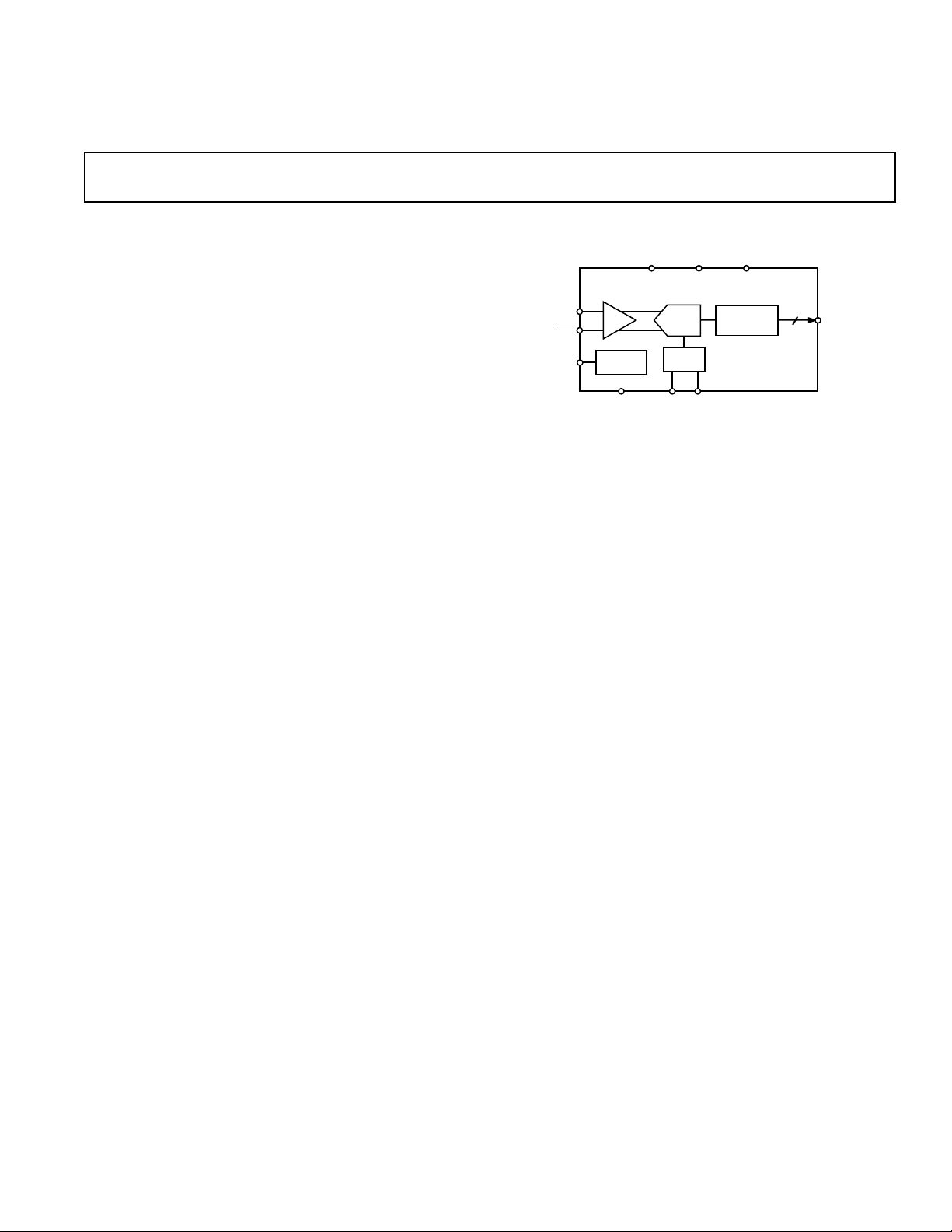
The AD9283 is an 8-bit monolithic sampling analog-to-digital
converter with an on-chip track-and-hold circuit and is optimized for low cost, low power, small size and ease of use. The
product operates at a 100 MSPS conversion rate, with outstanding dynamic performance over its full operating range.
The ADC requires only a single 3.0 V (2.7 V to 3.6 V) power
supply and an encode clock for full performance operation. No
external reference or driver components are required for many
applications. The digital outputs are TTL/CMOS compatible
and a separate output power supply pin supports interfacing
with 3.3 V or 2.5 V logic.
3 V A/D Converter
AD9283
FUNCTIONAL BLOCK DIAGRAM
The encoder input is TTL/CMOS compatible. A power-down
function may be exercised to bring total consumption to
4.2 mW. In power-down mode, the digital outputs are driven
to a high impedance state.
Fabricated on an advanced CMOS process, the AD9283 is
available in a 20-lead surface mount plastic package (SSOP)
specified over the industrial temperature range (–40°C to +85°C).
REV. C
Information furnished by Analog Devices is believed to be accurate and
reliable. However, no responsibility is assumed by Analog Devices for its
use, nor for any infringements of patents or other rights of third parties that
may result from its use. No license is granted by implication or otherwise
under any patent or patent rights of Analog Devices.
One Technology Way, P.O. Box 9106, Norwood, MA 02062-9106, U.S.A.
Tel: 781/329-4700 www.analog.com
Fax: 781/326-8703 © Analog Devices, Inc., 2001

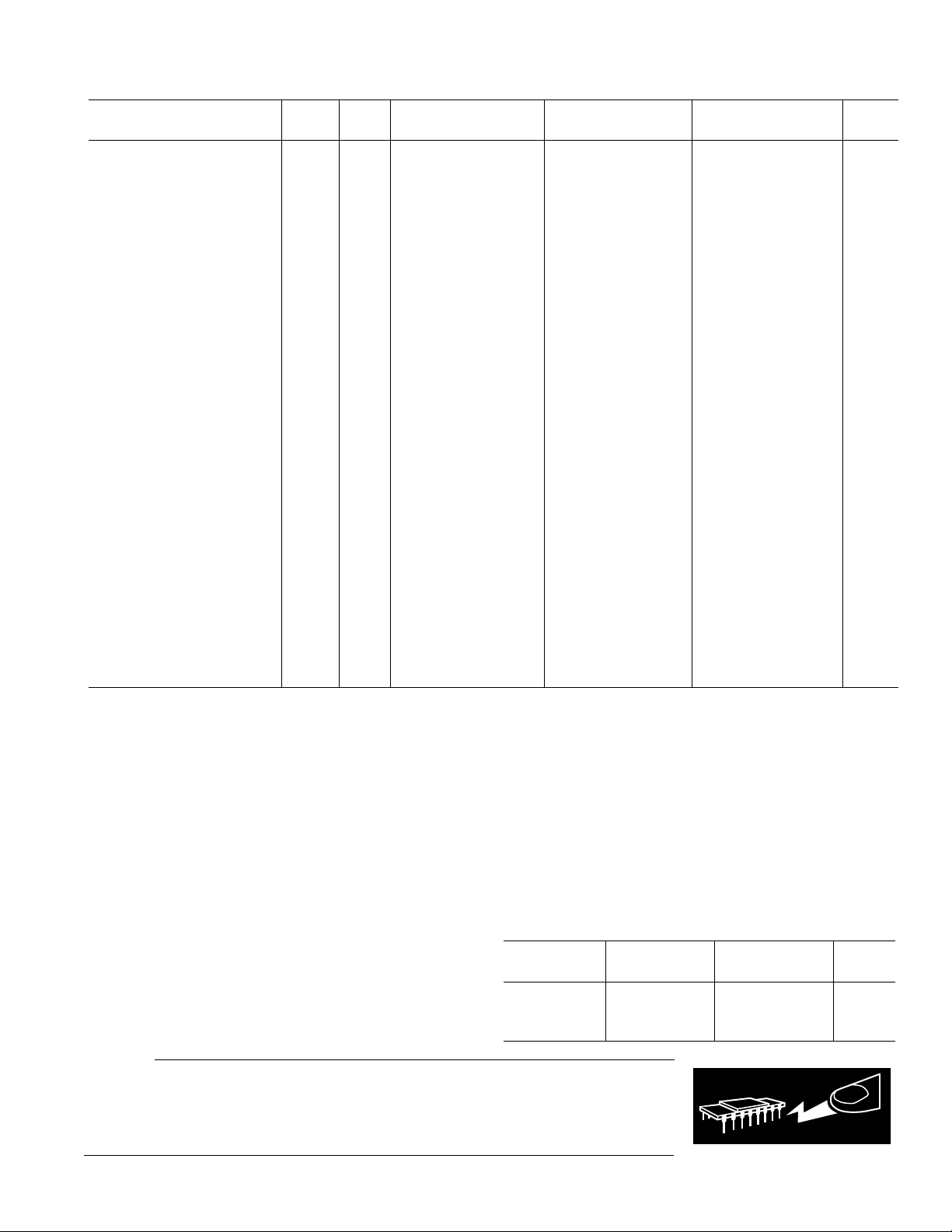
AD9283–SPECIFICATIONS
(VDD = 3.0 V, VD = 3.0 V; single-ended input; external reference, unless otherwise noted)
Test AD9283BRS-100 AD9283BRS-80 AD9283BRS-50
Parameter Temp Level Min Typ Max Min Typ Max Min Typ Max Unit
RESOLUTION 8 8 8 Bits
DC ACCURACY
Differential Nonlinearity 25°CI ± 0.5 +1.25 ± 0.5 +1.25 ±0.5 +1.25 LSB
Full VI +1.50 +1.50 +1.50 LSB
Integral Nonlinearity 25°C I –1.25 ± 0.75 +1.25 –1.25 ± 0.75 +1.25 –1.25 ± 0.75 +1.25 LSB
Full VI +2.25 +1.50 +1.50 LSB
No Missing Codes Full VI Guaranteed Guaranteed Guaranteed
Gain Error
Gain Tempco
1
1
25°CI –6 ± 2.5 +6 –6 ±2.5 +6 –6 ± 2.5 +6 % FS
Full VI –8 +8 –8 +8 –8 +8 % FS
Full VI 80 80 80 ppm/°C
ANALOG INPUT
Input Voltage Range
(With Respect to A
) Full V ±512 ±512 ±512 mV p-p
IN
Common-Mode Voltage Full V ± 200 ± 200 ± 200 mV
Input Offset Voltage 25°C I –35 ± 10 +35 –35 ± 10 +35 –35 ±10 +35 mV
Full VI ± 40 ± 40 ±40 mV
Reference Voltage Full VI 1.2 1.25 1.3 1.2 1.25 1.3 1.2 1.25 1.3 V
Reference Tempco Full VI ± 130 ± 130 ± 130 ppm/°C
Input Resistance 25°C I 7 10 13 7 10 13 7 10 13 kΩ
Full VI 5 16 5 16 5 16 kΩ
Input Capacitance 25°CV 2 2 2 pF
Full VI µA
Analog Bandwidth, Full Power 25°C V 475 475 475 MHz
SWITCHING PERFORMANCE
Maximum Conversion Rate Full VI 100 80 50 MSPS
Minimum Conversion Rate 25°CIV111MSPS
Encode Pulsewidth High (t
Encode Pulsewidth Low (t
Aperture Delay (t
)25°CV 0 0 0 ns
A
Aperture Uncertainty (Jitter) 25°C V 5 5 5 ps rms
Output Valid Time (t
)25°C IV 4.3 1000 5.0 1000 8.0 1000 ns
EH
)25°C IV 4.3 1000 5.0 1000 8.0 1000 ns
EL
2
)
V
Full VI 2.0 3.0 2.0 3.0 2.0 3.0 ns
Output Propagation Delay (tPD)2Full VI 4.5 7.0 4.5 7.0 4.5 7.0 ns
DIGITAL INPUTS
Logic “1” Voltage Full VI 2.0 2.0 2.0 V
Logic “0” Voltage Full VI 0.8 0.8 0.8 V
Logic “1” Current Full VI ± 1 ±1 ±1 µA
Logic “0” Current Full VI ± 1 ±1 ±1 µA
Input Capacitance 25°C V 2.0 2.0 2.0 pF
DIGITAL OUTPUTS
Logic “1” Voltage Full VI 2.95 2.95 2.95 V
Logic “0” Voltage Full VI 0.05 0.05 0.05 V
Output Coding Offset Binary Code Offset Binary Code Offset Binary Code
POWER SUPPLY
Power Dissipation
3, 4
Full VI 90 120 90 115 80 100 mW
Power-Down Dissipation Full VI 4.2 7 4.2 7 4.2 7 mW
Power Supply Rejection Ratio
(PSRR) 25°C I 18 18 18 mV/V
–2–
REV. C

AD9283
WARNING!
ESD SENSITIVE DEVICE
Test AD9283BRS-100 AD9283BRS-80 AD9283BRS-50
Parameter Temp Level Min Typ Max Min Typ Max Min Typ Max Unit
DYNAMIC PERFORMANCE
Transient Response 25°CV 2 2 2 ns
Overvoltage Recovery Time 25°CV 2 2 2 ns
Signal-to-Noise Ratio (SNR)
(Without Harmonics)
f
= 10.3 MHz 25°C I 46.5 47 44 47 dB
IN
= 27 MHz 25°C I 46.5 44 47 47 dB
f
IN
f
= 41 MHz 25°C I 43.5 46.5 47 dB
IN
= 76 MHz 25°C V 46.0 dB
f
IN
Signal-to-Noise Ratio (SINAD)
(With Harmonics)
f
= 10.3 MHz 25°C I 45 47 43.5 46.5 dB
IN
= 27 MHz 25°C I 45.5 43.5 46.5 46 dB
f
IN
f
= 41 MHz 25°C I 42.5 45 42 dB
IN
= 76 MHz 25°C V 42.5 dB
f
IN
Effective Number of Bits
= 10.3 MHz 25°C I 7.3 7.5 7.6 Bits
f
IN
f
= 27 MHz 25°C I 7.4 7.5 7.5 Bits
IN
= 41 MHz 25°C I 7.3 7.5 Bits
f
IN
f
= 76 MHz 25°C V 6.9 Bits
IN
2nd Harmonic Distortion
= 10.3 MHz 25°C I 57 60 55 60 dBc
f
IN
= 27 MHz 25°C I 60 55 60 56 dBc
f
IN
f
= 41 MHz 25°C I 50 58 55 dBc
IN
= 76 MHz 25°CV 46 dBc
f
IN
3rd Harmonic Distortion
= 10.3 MHz 25°C I 54.5 70 55 70 dBc
f
IN
f
= 27 MHz 25°C I 55 55 62.5 60 dBc
IN
= 41 MHz 25°C I 47 52.5 60 dBc
f
IN
f
= 76 MHz 25°CV 53 dBc
IN
Two-Tone Intermod Distortion
(IMD)
fIN = 10.3 MHz 25°C V 52 52 52 dBc
NOTES
1
Gain error and gain temperature coefficient are based on the ADC only (with a fixed 1.25 V external reference).
2
tV and tPD are measured from the 1.5 V level of the ENCODE input to the 50%/50% levels of the digital outputs swing. The digital output load during test is not to
exceed an ac load of 10 pF or a dc current of ± 40 µA.
3
Power dissipation measured with encode at rated speed and a dc analog input.
4
Typical thermal impedance for the RS style (SSOP) 20-lead package: θJC = 46°C/W, θCA = 80°C/W, θJA = 126°C/W.
5
SNR/harmonics based on an analog input voltage of –0.7 dBFS referenced to a 1.024 V full-scale input range.
Specifications subject to change without notice.
5
ABSOLUTE MAXIMUM RATINGS*
VD, VDD . . . . . . . . . . . . . . . . . . . . . . . . . . . . . . . . . . . . . . . 4 V
Analog Inputs . . . . . . . . . . . . . . . . . . . . –0.5 V to V
Digital Inputs . . . . . . . . . . . . . . . . . . . –0.5 V to V
VREF IN . . . . . . . . . . . . . . . . . . . . . . . . –0.5 V to V
+ 0.5 V
D
+ 0.5 V
DD
+ 0.5 V
D
Digital Output Current . . . . . . . . . . . . . . . . . . . . . . . . 20 mA
Operating Temperature . . . . . . . . . . . . . . . . –55°C to +125°C
Storage Temperature . . . . . . . . . . . . . . . . . . –65°C to +150°C
Maximum Junction Temperature . . . . . . . . . . . . . . . . 150°C
Maximum Case Temperature . . . . . . . . . . . . . . . . . . . 150°C
*Stresses above those listed under Absolute Maximum Ratings may cause perma-
nent damage to the device. This is a stress rating only; functional operation of the
device at these or any other conditions outside of those indicated in the operation
sections of this specification is not implied. Exposure to absolute maximum ratings
for extended periods may affect device reliability.
ORDERING GUIDE
Temperature Package Package
Model Ranges Descriptions Options
AD9283BRS
-50, -80, -100 –40°C to +85°C 20-Lead SSOP RS-20
AD9283/PCB 25°C Evaluation Board
CAUTION
ESD (electrostatic discharge) sensitive device. Electrostatic charges as high as 4000 V readily
accumulate on the human body and test equipment and can discharge without detection.
Although the AD9283 features proprietary ESD protection circuitry, permanent damage may
occur on devices subjected to high-energy electrostatic discharges. Therefore, proper ESD
precautions are recommended to avoid performance degradation or loss of functionality.
–3–REV. C

AD9283
EXPLANATION OF TEST LEVELS
Test Level
I 100% production tested.
II 100% production tested at 25°C and sample tested at
specified temperatures.
III Sample tested only.
IV Parameter is guaranteed by design and characteriza-
tion testing.
V Parameter is a typical value only.
VI 100% production tested at 25°C; guaranteed by design and
characterization testing for industrial temperature range;
100% production tested at temperature extremes for mili-
tary devices.
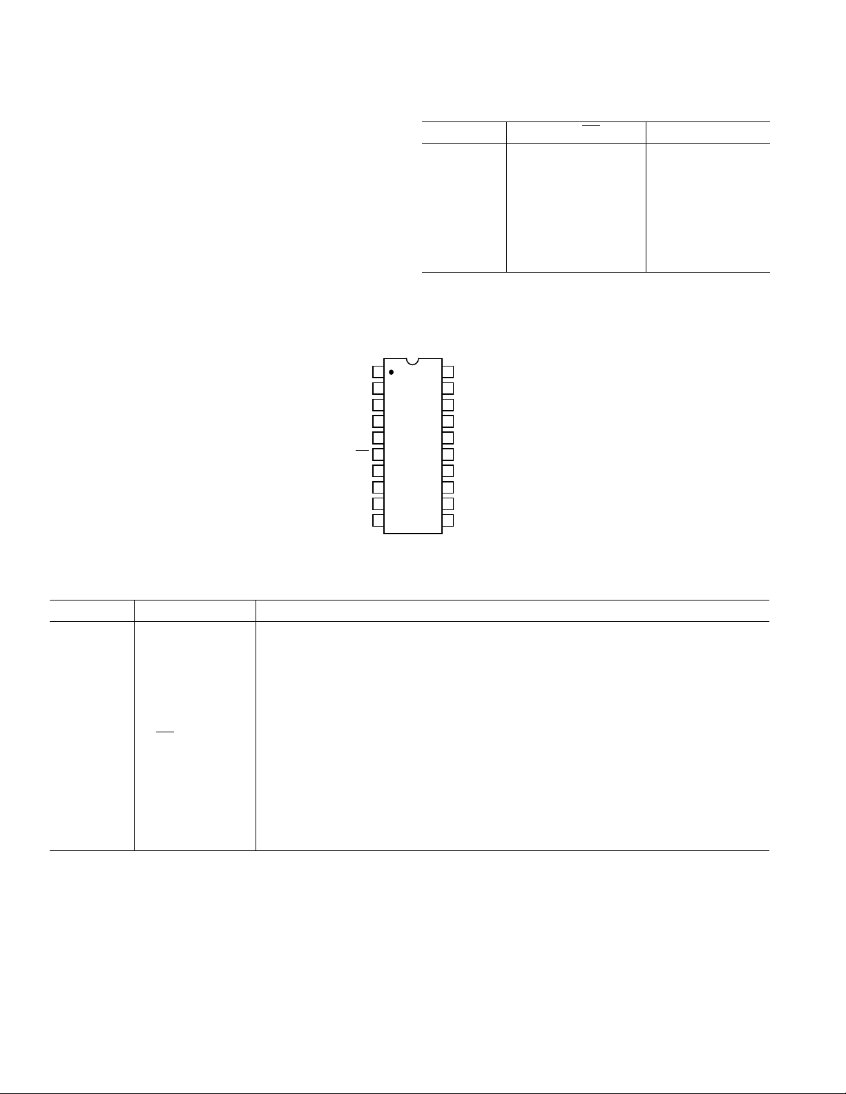
PIN CONFIGURATION
VREF IN
GND
A
A
GND
V
D
IN
IN
V
D
1
2
3
4
5
TOP VIEW
6
(Not to Scale)
7
8
9
10
PWRDWN
VREF OUT
ENCODE
Table I. Output Coding (VREF = 1.25 V)
Step AIN–A
IN
Digital Output
255 0.512 1111 1111
• ••
• ••
128 0.002 1000 0000
127 –0.002 0111 1111
• ••
• ••
0 –0.512 0000 0000
20
D0 (LSB)
19
D1
18
D2
17
D3
16
15
14
13
12
11
GND
V
DD
D4
D5
D6
D7 (MSB)
AD9283
PIN FUNCTION DESCRIPTIONS
Pin Number Mnemonic Function
1 PWRDWN Power-Down Function Select; Logic HIGH for Power-Down Mode (Digital Outputs Go
to High Impedance State)
2 VREF OUT Internal Reference Output (1.25 V typ); Bypass with 0.1 µF to Ground
3 VREF IN Reference Input for ADC (1.25 V typ)
4, 9, 16 GND Ground
5, 8 V
6A
D
IN
Analog 3 V Power Supply
Analog Input for ADC (Can Be Left Open if Operating in Single-Ended Mode, but Rec-
ommend Connection to a 0.1 µF Capacitor and a 25 Ω Resistor in Series to Ground for
Better Input Matching)
7A
IN
Analog Input for ADC
10 ENCODE Encode Clock for ADC (ADC Samples on Rising Edge of ENCODE)
11–14, 17–20 D7–D4, D3–D0 Digital Outputs of ADC
15 V
DD
Digital output power supply. Nominally 2.5 V to 3.6 V
–4–
REV. C
 Loading...