ANALOG DEVICES AD9273 Service Manual
Octal LNA/VGA/AAF/ADC
FEATURES
8 channels of LNA, VGA, AAF, and ADC
Low noise preamplifier (LNA)
Input-referred noise voltage = 1.26 nV/√Hz
(gain = 21.3 dB) @ 5 MHz typical
SPI-programmable gain = 15.6 dB/17.9 dB/21.3 dB
Single-ended input; V
550 mV p-p/367 mV p-p
Dual-mode active input impedance matching
Bandwidth (BW) > 100 MHz
Full-scale (FS) output = 4.4 V p-p differential
Variable gain amplifier (VGA)
Attenuator range = −42 dB to 0 dB
SPI-programmable PGA gain = 21 dB/24 dB/27 dB/30 dB
Linear-in-dB gain control
Antialiasing filter (AAF)
Programmable 2nd-order low-pass filter (LPF) from
8 MHz to 18 MHz
Programmable high-pass filter (HPF)
Analog-to-digital converter (ADC)
12 bits at 10 MSPS to 50 MSPS
SNR = 70 dB
SFDR = 75 dB
Serial LVDS (ANSI-644, IEEE 1596.3 reduced range link)
Data and frame clock outputs
Includes an 8 × 8 differential crosspoint switch to support
continuous wave (CW) Doppler
Low power, 109 mW per channel at 12 bits/40 MSPS (TGC)
70 mW per channel in CW Doppler
Flexible power-down modes
Overload recovery in <10 ns
Fast recovery from low power standby mode, <2 μs
100-lead TQFP and 144-ball BGA
APPLICATIONS
Medical imaging/ultrasound
Automotive radar
GENERAL DESCRIPTION
The AD9273 is designed for low cost, low power, small size, and
ease of use. It contains eight channels of a low noise preamplifier
(LNA) with a variable gain amplifier (VGA); an antialiasing
filter (AAF); and a 12-bit, 10 MSPS to 50 MSPS analog-todigital converter (ADC).
Each channel features a variable gain range of 42 dB, a fully
differential signal path, an active input preamplifier termination, a
maximum gain of up to 52 dB, and an ADC with a conversion
rate of up to 50 MSPS. The channel is optimized for dynamic
performance and low power in applications where a small
package size is critical.
maximum = 733 mV p-p/
IN
and Crosspoint Switch
AD9273
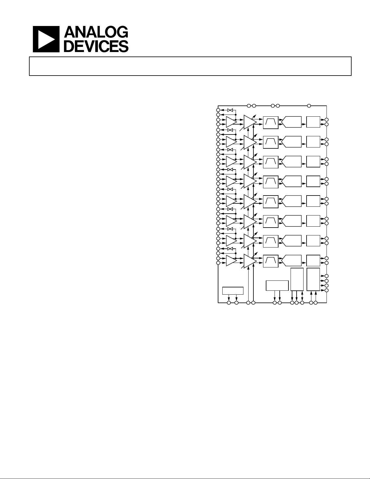
FUNCTIONAL BLOCK DIAGRAM
AVDD1
AVDD2
LOSW-A
LO-A
LI-A
LG-A
LOSW-B
LO-B
LI-B
LG-B
LOSW-C
LO-C
LI-C
LG-C
LOSW-D
LO-D
LI-D
LG-D
LOSW-E
LO-E
LI-E
LG-E
LOSW-F
LO-F
LI-F
LG-F
LOSW-G
LO-G
LI-G
LG-G
LOSW-H
LO-H
LI-H
LG-H
LNA
LNA
LNA
LNA
LNA
LNA
LNA
LNA
SWITCH
ARRAY
AND
CWD[7:0]+
VGA
VGA
VGA
VGA
VGA
VGA
VGA
VGA
GAIN–
GAIN+
CWD[7:0]–
The LNA has a single-ended-to-differential gain that is selectable
through the SPI. The LNA input-referred noise voltage is typically
1.26 nV/√Hz at a gain of 21.3 dB, and the combined input-referred
noise voltage of the entire channel is 1.42 nV/√Hz at typical
gain. Assuming a 15 MHz noise bandwidth (NBW) and a 21.3 dB
LNA gain, the input SNR is about 91 dB. In CW Doppler mode,
the LNA output drives a transconductance amp that is switched
through an 8 × 8 differential crosspoint switch. The switch is
programmable through the SPI.
STBY
PDWN
AAF
AAF
AAF
AAF
AAF
AAF
AAF
AAF
REFERENCE
VREF
RBIAS
Figure 1.
AD9273
12-BIT
ADC
12-BIT
ADC
12-BIT
ADC
12-BIT
ADC
12-BIT
ADC
12-BIT
ADC
12-BIT
ADC
12-BIT
ADC
SERIAL
CSB
DRVDD
SERIAL
LVDS
SERIAL
LVDS
SERIAL
LVDS
SERIAL
LVDS
SERIAL
LVDS
SERIAL
LVDS
SERIAL
LVDS
SERIAL
LVDS
DATA
PORT
INTERFACE
SDIO
SCLK
DOUTA+
DOUTA–
DOUTB+
DOUTB–
DOUTC+
DOUTC–
DOUTD+
DOUTD–
DOUTE+
DOUTE–
DOUTF+
DOUTF–
DOUTG+
DOUTG–
DOUTH+
DOUTH–
FCO+
FCO–
RATE
DCO+
MULTIPLIER
DCO–
CLK–
CLK+
07030-001
Rev. B
Information furnished by Analog Devices is believed to be accurate and reliable. However, no
responsibility is assumed by Analog Devices for its use, nor for any infringements of patents or other
rights of third parties that may result from its use. Specifications subject to change without notice. No
license is granted by implication or otherwise under any patent or patent rights of Analog Devices.
Trademarks and registered trademarks are the property of their respective owners.
One Technology Way, P.O. Box 9106, Norwood, MA 02062-9106, U.S.A.
Tel: 781.329.4700 www.analog.com
Fax: 781.461.3113 ©2009 Analog Devices, Inc. All rights reserved.

AD9273
TABLE OF CONTENTS
Features .............................................................................................. 1
Applications ....................................................................................... 1
General Description ......................................................................... 1
Functional Block Diagram .............................................................. 1
Revision History ............................................................................... 2
Product Highlights ........................................................................... 3
Specifications ..................................................................................... 4
AC Specifications .......................................................................... 4
Digital Specifications ................................................................... 8
Switching Specifications .............................................................. 9
ADC Timing Diagrams ................................................................. 10
Absolute Maximum Ratings .......................................................... 11
Thermal Impedance ................................................................... 11
ESD Caution ................................................................................ 11
Pin Configuration and Function Descriptions ........................... 12
Typical Performance Characteristics ........................................... 15
Equivalent Circuits ......................................................................... 19
Theory of Operation ...................................................................... 21
Ultrasound .................................................................................. 21
Channel Overview ..................................................................... 22
Input Overdrive .......................................................................... 25
CW Doppler Operation ............................................................. 25
TGC Operation ........................................................................... 27
ADC ............................................................................................. 31
Clock Input Considerations ...................................................... 31
Serial Port Interface (SPI) .............................................................. 38
Hardware Interface ..................................................................... 38
Memory Map .................................................................................. 40
Reading the Memory Map Table .............................................. 40
Reserved Locations .................................................................... 40
Default Values ............................................................................. 40
Logic Levels ................................................................................. 40
Outline Dimensions ....................................................................... 44
Ordering Guide .......................................................................... 45
REVISION HISTORY
7/09—Rev. A to Rev. B
Added BGA Package .......................................................... Universal
Changes to Features and General Description Sections .............. 1
Changes to Product Highlights Section ......................................... 3
Changes to Full-Channel (TGC) Characteristics Parameter,
Table 1 ............................................................................................ 4
Changes to Gain Control Interface Parameter and to CW
Doppler Mode Parameter, Table 1 .............................................. 6
Change to Wake-Up Time (Standby), GAIN+ = 0.8 V
Parameter ....................................................................................... 9
Changes to Figure 2 and Figure 3 ................................................. 10
Changes to Table 4 .......................................................................... 11
Addded Figure 5; Renumbered Sequentially .............................. 12
Changes to Table 6 .......................................................................... 13
Changes to Figure 34 and Figure 35 ............................................. 20
Changes to Ultrasound Section .................................................... 21
Changes to Low Noise Amplifier (LNA) Section ....................... 22
Changes to Active Impedance Matching Section and
Figure 40 ...................................................................................... 23
Changes to LNA Noise Section .................................................... 24
Changes to Input Overload Protection Section and Figure 44 ....... 25
Changes to Figure 48 ...................................................................... 28
Changes to Figure 49 and Figure 50............................................. 29
Changes to Clock Input Considerations Section and to
Figure 56 to Figure 59 ................................................................ 31
Changes to Digital Outputs and Timing Section ....................... 33
Changes to CSB Pin Section ......................................................... 36
Changes to Reading the Memory Map Table Section ............... 40
Updated Outline Dimensions ....................................................... 44
Changes to Ordering Guide .......................................................... 45
4/09—Revision A: Initial Version
Rev. B | Page 2 of 48

AD9273
The AD9273 requires a LVPECL-/CMOS-/LVDS-compatible
sample rate clock for full performance operation. No external
reference or driver components are required for many
applications.
The ADC automatically multiplies the sample rate clock for
the appropriate LVDS serial data rate. A data clock (DCO±) for
capturing data on the output and a frame clock (FCO±) trigger
for signaling a new output byte are provided.
Powering down individual channels is supported to increase
battery life for portable applications. There is also a standby
mode option that allows quick power-up for power cycling. In
CW Doppler operation, the VGA, AAF, and ADC are powered
down. The power of the time gain control (TGC) path scales
with selectable speed grades.
The ADC contains several features designed to maximize flexibility
and minimize system cost, such as a programmable clock, data
alignment, and programmable digital test pattern generation. The
digital test patterns include built-in fixed patterns, built-in
pseudorandom patterns, and custom user-defined test patterns
entered via the serial port interface.
Fabricated in an advanced CMOS process, the AD9273 is
available in a 16 mm × 16 mm, RoHS compliant, 100-lead
TQFP or a 144-ball BGA. It is specified over the industrial
temperature range of −40°C to +85°C.
PRODUCT HIGHLIGHTS
1. Small Footprint. Eight channels are contained in a small,
space-saving package. A full TGC path, ADC, and crosspoint
switch contained within a 100-lead, 16 mm × 16 mm TQFP or
a 144-ball BGA.
2. Low Power of 109 mW per Channel at 40 MSPS.
3. Integrated Crosspoint Switch. This switch allows numerous
multichannel configuration options to enable the CW
Doppler mode.
4. Ease of Use. A data clock output (DCO±) operates up to
300 MHz and supports double data rate (DDR) operation.
5. User Flexibility. Serial port interface (SPI) control offers a wide
range of flexible features to meet specific system requirements.
6. Integrated Second-Order Antialiasing Filter. This filter is
placed between the VGA and the ADC and is programmable
from 8 MHz to 18 MHz.
Rev. B | Page 3 of 48
AD9273
SPECIFICATIONS
AC SPECIFICATIONS
AVDD1 = 1.8 V, AVDD2 = 3.0 V, DRVDD = 1.8 V, 1.0 V internal ADC reference, fIN = 5 MHz, RS = 50 Ω, LNA gain = 21.3 dB, LNA bias =midhigh (default), PGA gain = 24 dB, GAIN− = 0.8 V, AAF LPF cutoff = f
ANSI-644 LVDS mode, unless otherwise noted.
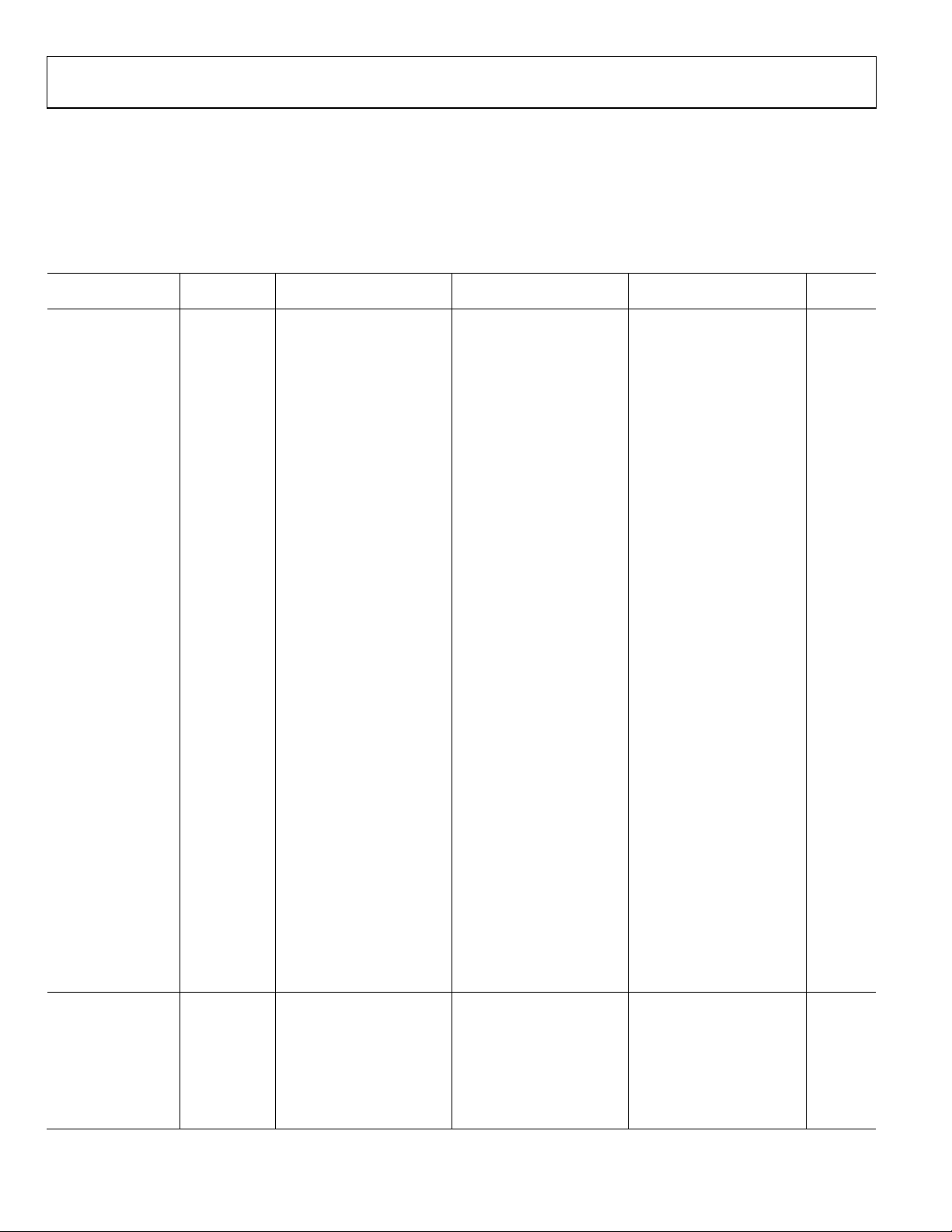
Table 1.
AD9273-25 AD9273-40 AD9273-50
Parameter
LNA CHARACTERISTICS
FULL-CHANNEL (TGC)
1
Gain Single-ended
Single-ended
Input Voltage Range LNA gain =
Input Common
Mode
Input Resistance RFB = 250 Ω 50 50 50 Ω
R
R
Input Capacitance LI-x 22 22 22 pF
−3 dB Bandwidth 70 70 70 MHz
Input-Referred
Noise Voltage
Input Noise Current RFB = ∞ 1 1 1 pA/√Hz
1 dB Input Com-
pression Point
Noise Figure LNA gain =
Active Termina-
tion Matched
Unterminated RFB = ∞ 6.3/5.3/4.4 6.3/5.3/4.4 6.3/5.3/4.4 dB
CHARACTERISTICS
AAF Low-Pass Filter
Cutoff
Out of range,3
Conditions Min Typ Max Min Typ Max Min Typ Max Unit
input to
differential
output
input to
single-ended
output
15.6 dB/
17.9 dB/
21.3 dB,
LNA output
limited to
4.4 V p-p
differential
output
0.9 0.9 0.9 V
= 500 Ω 100 100 100 Ω
FB
= ∞ 15 15 15 kΩ
FB
LNA gain =
15.6 dB/
17.9 dB/
21.3 dB,
R
= 0 Ω,
S
R
= ∞
FB
LNA gain =
15.6 dB/
17.9 dB/
21.3 dB,
GAIN+ = 0 V
15.6 dB/
17.9 dB/
21.3 dB
RS = 50 Ω,
= 200 Ω/
R
FB
250 Ω/350 Ω
In range, −3 dB,
programmable
−3 dB, programmable,
>>AAF bandwidth tolerance
15.6/17.9/21.3 15.6/17.9/21.3 15.6/17.9/21.3 dB
9.6/11.9/15.3 9.6/11.9/15.3 9.6/11.9/15.3 dB
733/550/367 733/550/367 733/550/367 mV p-p
1.6/1.42/1.26 1.6/1.42/1.26 1.6/1.42/1.26 nV/√Hz
1.0/0.8/0.5 1.0/0.8/0.5 1.0/0.8/0.5 mV p-p
5.8/5.1/4.3 5.8/5.1/4.3 5.8/5.1/4.3 dB
8 to 18 8 to 18 8 to 18 MHz
5 to 8, 18 to 35 5 to 8, 18 to 35 5 to 8, 18 to 35 MHz
/3 (default), HPF = LPF cutoff/20.7 (default), full temperature,
SAMPLE
2
SE
Rev. B | Page 4 of 48
AD9273
AD9273-25 AD9273-40 AD9273-50
Parameter
PGA GAIN Differential
1
AAF Bandwidth
Conditions Min Typ Max Min Typ Max Min Typ Max Unit
In range ±10 ±10 ±10 %
Tolerance
Group Delay
Variation
f = 1 MHz to
18 MHz,
±2 ±2 ±2 ns
GAIN+ = 0 V to
1.6 V
Input-Referred
Noise Voltage
LNA gain =
15.6 dB/
1.94/1.64/1.38 1.94/1.64/1.38 1.94/1.64/1.38 nV/√Hz
17.9 dB/
21.3 dB,
R
= ∞
FB
Noise Figure LNA gain =
15.6 dB/
17.9 dB/
21.3 dB
Active Termina-
tion Matched
RS = 50 Ω,
R
= 200 Ω/
FB
10.3/8.7/6.8 10.3/8.6/6.7 10.3/8.6/6.7 dB
250 Ω/350 Ω
Unterminated RFB = ∞ 7.1/6.0/4.8 7.1/5.9/4.8 7.1/5.9/4.8 dB
Correlated Noise
Ratio
No signal,
correlated/
−30 −30 −30 dB
uncorrelated
Output Offset −35 +35 −35 +35 −35 +35 LSB
Signal-to-Noise
Ratio (SNR)
fIN = 5 MHz at
−10 dBFS,
65.5 64 63.5 dBFS
GAIN+ = 0 V
f
= 5 MHz at
IN
58.5 57 56.5 dBFS
−1 dBFS,
GAIN+ = 1.6 V
Harmonic Distortion
Second
Harmonic
fIN = 5 MHz at
−10 dBFS,
−55 −52 −52 dBc
GAIN+ = 0 V
f
= 5 MHz at
IN
−67 −62 −58 dBc
−1 dBFS,
GAIN+ = 1.6 V
Third Harmonic fIN = 5 MHz at
−56 −50 −47 dBc
−10 dBFS,
GAIN+ = 0 V
f
= 5 MHz at
IN
−61 −56 −55 dBc
−1 dBFS,
GAIN+ = 1.6 V
Two-Tone IMD3
(2 × F1 − F2)
Distortion
f
= 5.0 MHz at
IN1
−1 dBFS,
f
= 5.01 MHz
IN2
−75 −75 −75 dBc
at −21 dBFS,
GAIN+ = 1.6 V,
LNA gain =
21.3 dB
Channel-to-Channel
Crosstalk
Overrange
Channel-to-Channel
Delay Variation
f
= 5.0 MHz at
IN1
−1 dBFS
condition
4
Full TGC path,
= 5 MHz,
f
IN
−70 −70 −70 dB
−65 −65 −65 dB
0.3 0.3 0.3 Degrees
GAIN+ = 0 V to
1.6 V
21/24/27/30 21/24/27/30 21/24/27/30 dB
input to
differential
output
Rev. B | Page 5 of 48

AD9273
AD9273-25 AD9273-40 AD9273-50
Parameter
GAIN ACCURACY 25°C
1.44 V < GAIN+
GAIN CONTROL
CW DOPPLER MODE
POWER SUPPLY
1
Gain Law Confor-
mance Error
0.16 V < GAIN+
Conditions Min Typ Max Min Typ Max Min Typ Max Unit
0 V < GAIN+
1.5 1.5 1.5 dB
< 0.16 V
−1.6 +1.6 −1.6 +1.6 −1.7 +1.7 dB
< 1.44 V
−2.5 −2.5 −2.5 dB
< 1.6 V
Linear Gain Error GAIN+ = 0.8 V,
−1.6 +1.6 −1.6 +1.6 −1.7 +1.7 dB
normalized for
ideal AAF loss
Channel-to-Channel
Matching
0.16 V < GAIN+
< 1.44 V
0.1 0.1 0.1 dB
INTERFACE
Normal Operating
0 1.6 0 1.6 0 1.6 V
Range
Gain Range GAIN+ =
42 42 42 dB
0 V to 1.6 V
Scale Factor 28 28 28 dB/V
Response Time 42 dB change 750 750 750 ns
Gain+ Impedance Single ended 10 10 10 MΩ
Gain− Impedance Single ended 70 70 70 kΩ
Transconductance Differential,
5.4/7.3/10.9 5.4/7.3/10.9 5.4/7.3/10.9 mA/V
LNA gain =
15.6 dB/
17.9 dB/
21.3 dB
Output Level Range Differential,
1.5 3.6 1.5 3.6 1.5 3.6 V
CW Doppler
output pins
Input-Referred
Noise Voltage
LNA gain =
15.6 dB/
2.6/2.1/1.6 2.6/2.1/1.6 2.6/2.1/1.6 nV/√Hz
17.9 dB/
21.3 dB,
R
= 0 Ω,
S
R
= ∞,
FB
= 675 Ω
R
L
Input-Referred
Dynamic Range
LNA gain =
15.6 dB/
160/159/158 160/159/158 160/159/158 dBFS/√Hz
17.9 dB/
21.3 dB,
R
= 0 Ω,
S
= ∞
R
FB
Two-Tone IMD3
(2 × F1 − F2)
Distortion
f
= 5.0 MHz at
IN1
−1 dBFS (FS at
LNA input), f
−70 −70 −70 dBc
=
IN2
5.01 MHz at
−21 dBFS (FS at
LNA input), LNA
gain = 21.3 dB
Output DC Bias Single ended,
2.4 2.4 2.4 mA
per channel
Maximum Output
Swing
Single ended,
per channel
±2 ±2 ±2 mA p-p
AVDD1 1.7 1.8 1.9 1.7 1.8 1.9 1.7 1.8 1.9 V
AVDD2 2.7 3.0 3.6 2.7 3.0 3.6 2.7 3.0 3.6 V
DRVDD 1.7 1.8 1.9 1.7 1.8 1.9 1.7 1.8 1.9 V
I
Full-channel
AVDD1
158 186 223 mA
mode
CW Doppler
32 32 32 mA
mode with four
channels
enabled
Rev. B | Page 6 of 48
AD9273
AD9273-25 AD9273-40 AD9273-50
Parameter
ADC RESOLUTION 12 12 12 Bits
ADC REFERENCE
1
See the AN-835 Application Note, Understanding High Speed ADC Testing and Evaluation, for a complete set of definitions and how these tests were completed.
2
SE = single ended.
3
AAF settings < 5 MHz are out of range and are not supported.
4
The overrange condition is specified as being 6 dB more than the full-scale input range.
1
I
Full-channel
AVDD2
Conditions Min Typ Max Min Typ Max Min Typ Max Unit
150 150 150 mA
mode
CW Doppler
70 70 70 mA
mode with four
channels
enabled
I
47 49 50 mA
DRVDD
Total Power
Dissipation
Includes output
drivers, fullchannel mode,
819 940 873 996 943 1072 mW
no signal
CW Doppler
275 275 275 mW
mode with four
channels
enabled
Power-Down
5 5 5 mW
Dissipation
Standby Power
148 158 170 mW
Dissipation
Power Supply
1.6 1.6 1.6 mV/V
Rejection Ratio
(PSRR)
Output Voltage Error VREF = 1 V ±20 ±20 ±20 mV
Load Regulation At 1.0 mA,
2 2 2 mV
VREF = 1 V
Input Resistance 6 6 6 kΩ
Rev. B | Page 7 of 48

AD9273
DIGITAL SPECIFICATIONS
AVDD1 = 1.8 V, AVDD2 = 3.0 V, DRVDD = 1.8 V, 1.0 V internal ADC reference, fIN = 5 MHz, full temperature, unless otherwise noted.
Table 2.
1
Parameter
Temperature Min Typ Max Unit
CLOCK INPUTS (CLK+, CLK−)
Logic Compliance CMOS/LVDS/LVPECL
Differential Input Voltage
2
Full 250 mV p-p
Input Common-Mode Voltage Full 1.2 V
Input Resistance (Differential) 25°C 20 kΩ
Input Capacitance 25°C 1.5 pF
LOGIC INPUTS (PDWN, STBY, SCLK)
Logic 1 Voltage Full 1.2 3.6 V
Logic 0 Voltage Full 0.3 V
Input Resistance 25°C 30 kΩ
Input Capacitance 25°C 0.5 pF
LOGIC INPUT (CSB)
Logic 1 Voltage Full 1.2 3.6 V
Logic 0 Voltage Full 0.3 V
Input Resistance 25°C 70 kΩ
Input Capacitance 25°C 0.5 pF
LOGIC INPUT (SDIO)
Logic 1 Voltage Full 1.2 DRVDD + 0.3 V
Logic 0 Voltage Full 0 0.3 V
Input Resistance 25°C 30 kΩ
Input Capacitance 25°C 2 pF
LOGIC OUTPUT (SDIO)
3
Logic 1 Voltage (IOH = 800 A) Full 1.79 V
Logic 0 Voltage (IOL = 50 A) Full 0.05 V
DIGITAL OUTPUTS (DOUTx+, DOUTx−) IN ANSI-644 MODE
1
Logic Compliance LVDS
Differential Output Voltage (VOD) Full 247 454 mV
Output Offset Voltage (VOS) Full 1.125 1.375 V
Output Coding (Default) Offset binary
DIGITAL OUTPUTS (DOUTx+, DOUTx−) WITH
LOW POWER, REDUCED-SIGNAL OPTION
1
Logic Compliance LVDS
Differential Output Voltage (VOD) Full 150 250 mV
Output Offset Voltage (VOS) Full 1.10 1.30 V
Output Coding (Default) Offset binary
1
See the AN-835 Application Note, Understanding High Speed ADC Testing and Evaluation, for a complete set of definitions and how these tests were completed.
2
Specified for LVDS and LVPECL only.
3
Specified for 13 SDIO pins sharing the same connection.
Rev. B | Page 8 of 48
AD9273
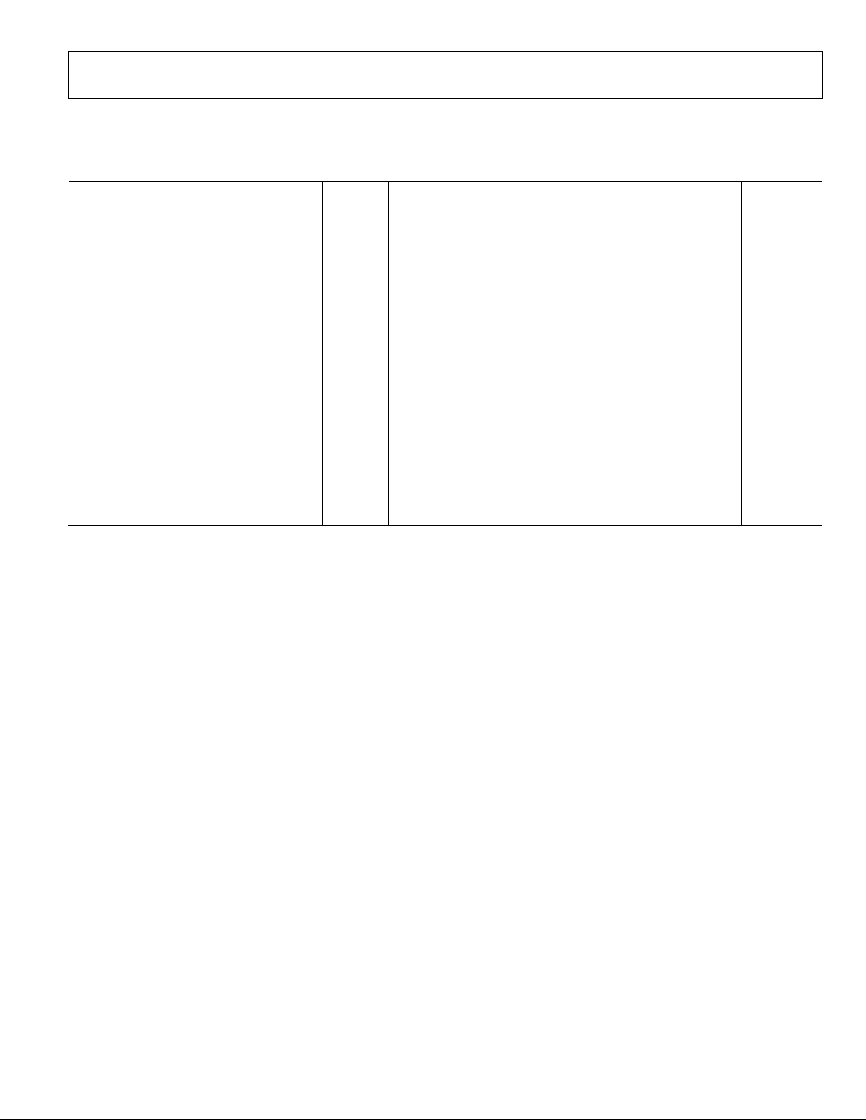
SWITCHING SPECIFICATIONS
AVDD1 = 1.8 V, AVDD2 = 3.0 V, DRVDD = 1.8 V, 1.0 V internal ADC reference, fIN = 5 MHz, full temperature, unless otherwise noted.
Table 3.
1
Parameter
CLOCK
2
Temp Min Typ Max Unit
Clock Rate Full 10 50 MSPS
Clock Pulse Width High (tEH) Full 10 ns
Clock Pulse Width Low (tEL) Full 10 ns
2, 3
OUTPUT PARAMETERS
Propagation Delay (tPD) Full (t
Rise Time (tR) (20% to 80%) Full
Fall Time (tF) (20% to 80%) Full
FCO± Propagation Delay (t
DCO± Propagation Delay (t
DCO± to Data Delay (t
DCO± to FCO± Delay (t
Data-to-Data Skew
DATA -MAX
− t
DATA -MIN
(t
Wake-Up Time (Standby), GAIN+ = 0.8 V 25°C
Wake-Up Time (Power-Down) 25°C
Pipeline Latency Full
APERTURE
Aperture Uncertainty (Jitter) 25°C
1
See the AN-835 Application Note, Understanding High Speed ADC Testing and Evaluation, for a complete set of definitions and how these tests were completed.
2
Can be adjusted via the SPI.
3
Measurements were made using a part soldered to FR-4 material.
4
t
/24 is based on the number of bits divided by 2 because the delays are based on half duty cycles.
SAMPLE
) Full (t
FCO
4
)
Full t
CPD
4
)
Full (t
DATA
4
)
Full (t
FRAME
)
Full
/2) + 1.5 (t
SAMPLE
300
300
/2) + 1.5 (t
SAMPLE
/24) − 300 (t
SAMPLE
/24) − 300 (t
SAMPLE
±100 ±350
<2
1
8
<1
/2) + 2.3 (t
SAMPLE
/2) + 2.3 (t
SAMPLE
+ (t
FCO
SAMPLE
/24) (t
SAMPLE
/24) (t
SAMPLE
/2) + 3.1 ns
SAMPLE
ps
ps
/2) + 3.1 ns
SAMPLE
/24) ns
/24) + 300 ps
SAMPLE
/24) + 300 ps
SAMPLE
ps
µs
ms
Clock cycles
ps rms
Rev. B | Page 9 of 48
AD9273
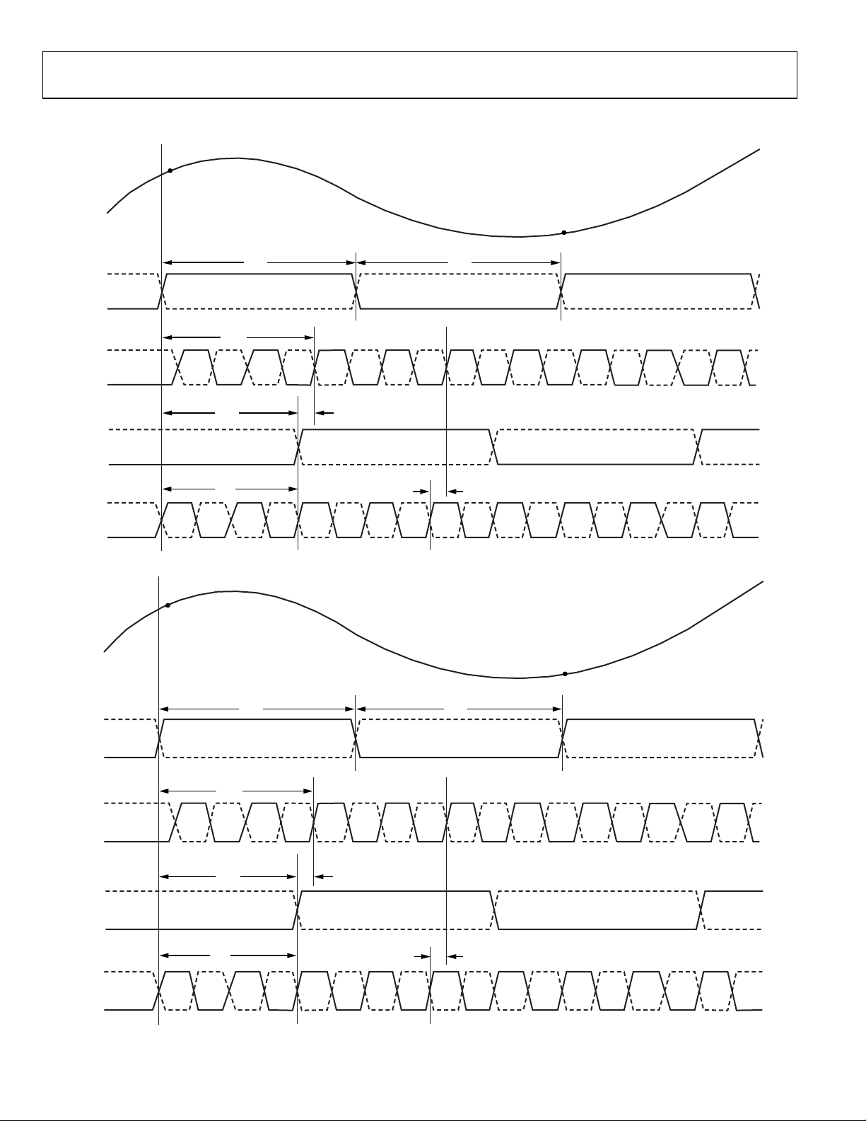
ADC TIMING DIAGRAMS
N – 1
AIN
N
CLK–
CLK+
DCO–
DCO+
FCO–
FCO+
DOUTx–
DOUTx+
AIN
N – 1
t
FCO
t
t
EH
t
CPD
t
FRAME
PD
MSB
D10
N – 8
N – 8D9N – 8D8N – 8D7N – 8D6N – 8D5N – 8D4N – 8D3N – 8D2N – 8D1N – 8D0N – 8
t
EL
t
DATA
D10
MSB
N – 7
N – 7
07030-002
Figure 2. 12-Bit Data Serial Stream (Default)
N
CLK–
CLK+
DCO–
DCO+
FCO–
FCO+
DOUTx–
DOUTx+
t
EH
t
CPD
t
FCO
t
PD
t
FRAME
D0
(LSB)D1N – 8D2N – 8D3N – 8D4N – 8D5N – 8D6N – 8D7N – 8D8N – 8D9N – 8
t
EL
t
DATA
D10
D11
N – 8
(MSB)
07030-004
Figure 3. 12-Bit Data Serial Stream, LSB First
Rev. B | Page 10 of 48
AD9273
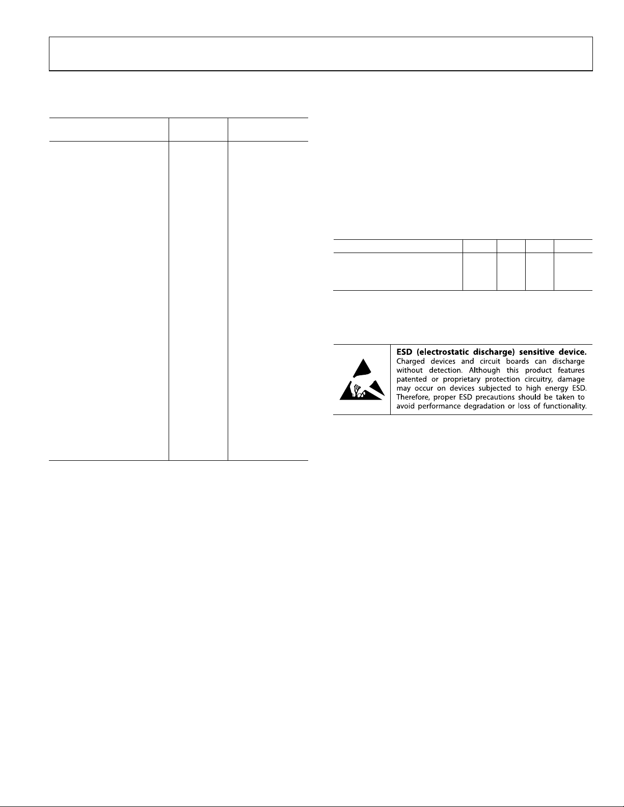
ABSOLUTE MAXIMUM RATINGS
Table 4.
With
Parameter
Electrical
AVDD1 GND −0.3 V to +2.0 V
AVDD2 GND −0.3 V to +3.9 V
DRVDD GND −0.3 V to +2.0 V
GND GND −0.3 V to +0.3 V
AVDD2 AVDD1 −2.0 V to +3.9 V
AVDD2 DRVDD −2.0 V to +3.9 V
AVDD1 DRVDD −2.0 V to +2.0 V
Digital Outputs
(DOUTx+, DOUTx−,
DCO+, DCO−,
FCO+, FCO−)
CLK+, CLK−, GAIN+,
GAIN−
LI-x, LO-x, LOSW-x LG-x −0.3 V to +2.0 V
CWDx−, CWDx+ GND −0.3 V to +3.9 V
PDWN, STBY, SCLK, CSB GND −0.3 V to +3.9 V
RBIAS, VREF, SDIO GND −0.3 V to +2.0 V
Environmental
Operating Temperature
Range (Ambient)
Storage Temperature
Range (Ambient)
Maximum Junction
Temperature
Lead Temperature
(Soldering, 10 sec)
Respect To Rating
GND −0.3 V to +2.0 V
GND −0.3 V to +3.9 V
−40°C to +85°C
−65°C to +150°C
150°C
300°C
Stresses above those listed under Absolute Maximum Ratings
may cause permanent damage to the device. This is a stress
rating only; functional operation of the device at these or any
other conditions above those indicated in the operational
section of this specification is not implied. Exposure to absolute
maximum rating conditions for extended periods may affect
device reliability.
THERMAL IMPEDANCE
Table 5.
Airflow Velocity (m/sec) θ
0.0 20.3 N/A N/A °C/W
1.0 14.4 7.6 4.7 °C/W
2.5 12.9 N/A N/A °C/W
1
θJA is for a 4-layer PCB with a solid ground plane (simulated). The exposed
pad is soldered to the PCB.
1
θ
JA
θJC Unit
JB
ESD CAUTION
Rev. B | Page 11 of 48
AD9273
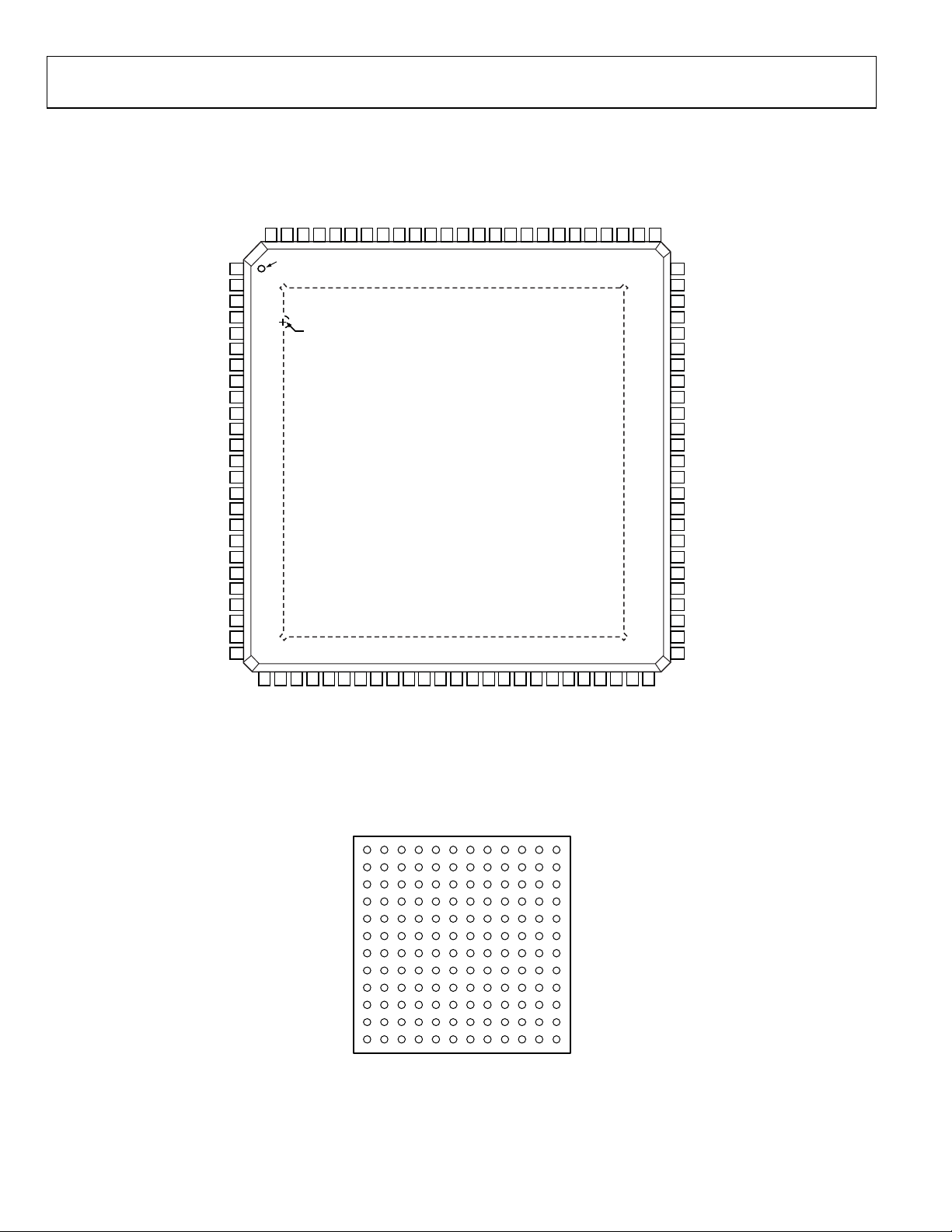
PIN CONFIGURATION AND FUNCTION DESCRIPTIONS
LOSW-DLO-D
CWD0–
CWD0+
CWD1–
CWD1+
CWD2–
CWD2+
CWD3–
CWD3+
AVDD2
GAIN–
GAIN+
VREF
RBIAS
CWD4–
AD9273
TOP VIEW
(Not to Scale)
76
LI-D
75
LG-D
74
AVDD2
73
AVDD1
72
LO-C
71
LOSW-C
70
LI-C
69
LG-C
68
AVDD2
67
AVDD1
66
LO-B
65
64
LOSW-B
63
LI-B
LG-B
62
AVDD2
61
AVDD1
60
59
LO-A
58
LOSW-A
57
LI-A
LG-A
56
AVDD2
55
54
AVDD1
53
CSB
52
SDIO
51
SCLK
LI-E
LG-E
AVDD2
AVDD1
LO-F
LOSW-F
LI-F
LG-F
AVDD2
AVDD1
LO-G
LOSW-G
LI-G
LG-G
AVDD2
AVDD1
LO-H
LOSW-H
LI-H
LG-H
AVDD2
AVDD1
CLK–
CLK+
AVDD1
CWD5–
CWD5+
CWD6–
CWD6+
CWD7–
CWD7+
LO-E
LOSW-E
9998979695949392919089888786858483828180797877
100
PIN 1
1
INDICATOR
2
3
4
5
6
7
8
9
10
11
12
13
14
15
16
17
18
19
20
21
22
23
24
25
EXPOSED PADDLE, PIN 0
(BOTTOM OF PACKAGE)
CWD4+
2627282930313233343536373839404142434445464748
FCO–
DRVDD
DOUTH–
DOUTH+
DOUTG–
NOTES
1. THE EXPOSED PAD SHOULD BE T IED TO A QUIET ANALOG GROUND.
DOUTF+
DOUTG+
DOUTF–
DCO–
DOUTE–
DOUTE+
FCO+
DCO+
DOUTD–
DOUTD+
DOUTC–
DOUTC+
DOUTA+
DOUTB+
DRVDD
DOUTA–
DOUTB–
50
49
STBY
PDWN
AVDD1
07030-005
Figure 4. TQFP Pin Configuration
4
2
1357
A
B
C
D
E
F
G
H
J
K
L
M
(Not to S cale)
Figure 5. BGA Pin Configuration
6
TOP VIEW
10 12
8
9
11
07030-300
Rev. B | Page 12 of 48
AD9273
Table 6. Pin Function Descriptions
Pin No.
TQFP BGA Name Description
0 N/A GND Ground (the exposed paddle should be tied to a quiet analog ground)
N/A
4, 10, 16, 22,
25, 50, 54, 60,
66, 72
3, 9, 15, 21, 55,
61, 67, 73, 86
26, 47 L1, L12 DRVDD 1.8 V Digital Output Driver Supply
1 A1 LI-E LNA Analog Input for Channel E
2 B1 LG-E LNA Ground for Channel E
5 C2 LO-F LNA Analog Inverted Output for Channel F
6 D2 LOSW-F LNA Analog Switched Output for Channel F
7 A2 LI-F LNA Analog Input for Channel F
8 B2 LG-F LNA Ground for Channel F
11 C3 LO-G LNA Analog Inverted Output for Channel G
12 D3 LOSW-G LNA Analog Switched Output for Channel G
13 A3 LI-G LNA Analog Input for Channel G
14 B3 LG-G LNA Ground for Channel G
17 C4 LO-H LNA Analog Inverted Output for Channel H
18 D4 LOSW-H LNA Analog Switched Output for Channel H
19 A4 LI-H LNA Analog Input for Channel H
20 B4 LG-H LNA Ground for Channel H
23 H1 CLK− Clock Input Complement
24 J1 CLK+ Clock Input True
27 M2 DOUTH− ADC H Digital Output Complement
28 L2 DOUTH+ ADC H Digital Output True
29 M3 DOUTG− ADC G Digital Output Complement
30 L3 DOUTG+ ADC G Digital Output True
31 M4 DOUTF− ADC F Digital Output Complement
32 L4 DOUTF+ ADC F Digital Output True
33 M5 DOUTE− ADC E Digital Output Complement
34 L5 DOUTE+ ADC E Digital Output True
35 M6 DCO− Digital Clock Output Complement
36 L6 DCO+ Digital Clock Output True
37 M7 FCO− Frame Clock Digital Output Complement
38 L7 FCO+ Frame Clock Digital Output True
39 M8 DOUTD− ADC D Digital Output Complement
40 L8 DOUTD+ ADC D Digital Output True
41 M9 DOUTC− ADC C Digital Output Complement
42 L9 DOUTC+ ADC C Digital Output True
43 M10 DOUTB− ADC B Digital Output Complement
44 L10 DOUTB+ ADC B Digital Output True
B5, B6, B8, C5,
C6, C7, C8, D5,
D6, D7, D8, E1,
E5, E6, E7, E8,
E12, F2, F4, F6,
F7, F9, F11, G1,
G3, G5, G6, G7,
G8, G10, G12,
H2, H3, H4, H5,
H6, H7, H8, H9,
H10, H11, J2,
K1, K2, M1, M12
F1, F3, F5, F8,
F10, F12, G2,
G4, G9, G11
B7, E2, E3, E4,
E9, E10, E11
GND Ground
AVDD1 1.8 V Analog Supply
AVDD2 3.0 V Analog Supply
Rev. B | Page 13 of 48
AD9273
Pin No.
TQFP BGA Name Description
45 M11 DOUTA− ADC A Digital Output Complement
46 L11 DOUTA+ ADC A Digital Output True
48 K11 STBY Standby Power-Down
49 J11 PDWN Full Power-Down
51 K12 SCLK Serial Clock
52 J12 SDIO Serial Data Input/Output
53 H12 CSB Chip Select Bar
56 B9 LG-A LNA Ground for Channel A
57 A9 LI-A LNA Analog Input for Channel A
58 D9 LOSW-A LNA Analog Switched Output for Channel A
59 C9 LO-A LNA Analog Inverted Output for Channel A
62 B10 LG-B LNA Ground for Channel B
63 A10 LI-B LNA Analog Input for Channel B
64 D10 LOSW-B LNA Analog Switched Output for Channel B
65 C10 LO-B LNA Analog Inverted Output for Channel B
68 B11 LG-C LNA Ground for Channel C
69 A11 LI-C LNA Analog Input for Channel C
70 D11 LOSW-C LNA Analog Switched Output for Channel C
71 C11 LO-C LNA Analog Inverted Output for Channel C
74 B12 LG-D LNA Ground for Channel D
75 A12 LI-D LNA Analog Input for Channel D
76 D12 LOSW-D LNA Analog Switched Output for Channel D
77 C12 LO-D LNA Analog Inverted Output for Channel D
78 K10 CWD0− CW Doppler Output Complement for Channel 0
79 J10 CWD0+ CW Doppler Output True for Channel 0
80 K9 CWD1− CW Doppler Output Complement for Channel 1
81 J9 CWD1+ CW Doppler Output True for Channel 1
82 K8 CWD2− CW Doppler Output Complement for Channel 2
83 J8 CWD2+ CW Doppler Output True for Channel 2
84 K7 CWD3− CW Doppler Output Complement for Channel 3
85 J7 CWD3+ CW Doppler Output True for Channel 3
87 A8 GAIN− Gain Control Voltage Input Complement
88 A7 GAIN+ Gain Control Voltage Input True
89 A6 RBIAS External Resistor to Set the Internal ADC Core Bias Current
90 A5 VREF Voltage Reference Input/Output
91 K6 CWD4− CW Doppler Output Complement for Channel 4
92 J6 CWD4+ CW Doppler Output True for Channel 4
93 K5 CWD5− CW Doppler Output Complement for Channel 5
94 J5 CWD5+ CW Doppler Output True for Channel 5
95 K4 CWD6− CW Doppler Output Complement for Channel 6
96 J4 CWD6+ CW Doppler Output True for Channel 6
97 K3 CWD7− CW Doppler Output Complement for Channel 7
98 J3 CWD7+ CW Doppler Output True for Channel 7
99 C1 LO-E LNA Analog Inverted Output for Channel E
100 D1 LOSW-E LNA Analog Switched Output for Channel E
Rev. B | Page 14 of 48
AD9273
TYPICAL PERFORMANCE CHARACTERISTICS
f
= 40 MSPS, fIN = 5 MHz, RS = 50 Ω, LNA gain = 21.3 dB, LNA bias = mid-high, PGA gain = 24 dB, AAF LPF cutoff = f
SAMPLE
HPF = LPF cutoff/20.7 (default), GAIN− = 0.8 V
2.0
14
SAMPLE
/3,
1.5
1.0
0.5
0
–0.5
GAIN ERROR (dB)
–1.0
–1.5
–2.0
0 0.2 0.4 0.6 0.8 1.0
–40°C
+25°C
+85°C
GAIN+ (V)
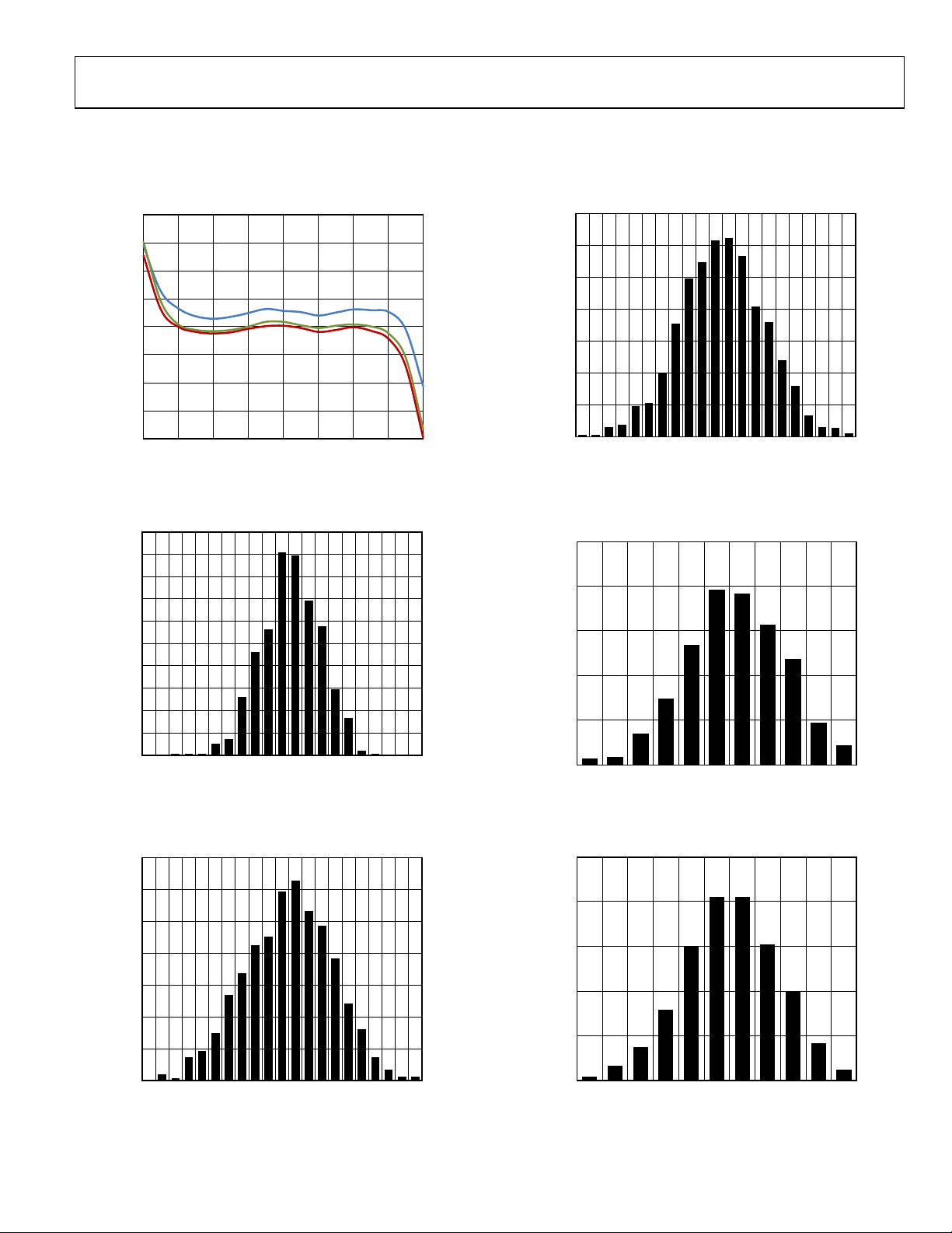
Figure 6. Gain Error vs. GAIN+ at Three Temperatures
20
18
16
14
12
10
8
6
PERCENTAGE OF UNITS (%)
4
2
0
–1.0
–0.9
–0.8
–0.7
–0.6
–0.5
–0.4
0
–0.3
GAIN ERROR (dB)
0.1
–0.2
–0.1
0.2
0.3
Figure 7. Gain Error Histogram, GAIN+ = 0.16 V
1.2 1.4 1.6
0.4
0.5
0.6
0.7
0.8
12
10
8
6
4
PERCENTAGE OF UNITS (%)
2
0
–1.0
–0.9
–0.8
–0.7
–0.6
–0.5
07030-114
–0.4
0
–0.3
GAIN ERROR (dB)
0.1
–0.2
–0.1
0.2
0.3
0.4
0.5
0.6
0.7
0.8
0.9
1.0
07030-186
Figure 9. Gain Error Histogram, GAIN+ = 1.44 V
25
20
15
10
PERCENTAGE OF UNITS (%)
5
0.9
1.0
07030-184
0
–1.25 –1.00 –0.75
–0.50 –0.25 0
CHANNEL-TO-CHANNEL GAIN MATCHI NG (dB)
0.25 0.50 0.75 1.00 1.25
07030-180
Figure 10. Gain Match Histogram, GAIN+ = 0.3 V
14
12
10
8
6
4
PERCENTAGE OF UNITS (%)
2
0
–1.0
–0.9
–0.8
–0.7
–0.6
–0.5
–0.4
0
–0.3
–0.2
–0.1
GAIN ERROR (dB)
Figure 8. Gain Error Histogram, GAIN+ = 0.8 V
25
20
15
10
PERCENTAGE OF UNITS (%)
5
0
0.1
0.2
0.3
0.4
0.5
0.6
0.7
0.8
0.9
1.0
07030-185
–1.25 –1.00 –0.75
Figure 11. Gain Match Histogram, GAIN+ = 1.3 V
–0.50 –0.25 0
CHANNEL-TO-CHANNEL GAIN MATCHI NG (dB)
0.25 0.50 0.75 1.00 1.25
07030-181
Rev. B | Page 15 of 48
 Loading...