Octal LNA/VGA/AAF/ADC
www.BDTIC.com/ADI
and Crosspoint Switch
FEATURES
8 channels of LNA, VGA, AAF, and ADC
Low noise preamplifier (LNA)
Input-referred noise voltage = 0.75 nV/√Hz
(gain = 21.3 dB) @ 5 MHz typical
SPI-programmable gain = 15.6 dB/17.9 dB/21.3 dB
Single-ended input; V
maximum = 733 mV p-p/
IN
550 mV p-p/367 mV p-p
Dual-mode active input impedance matching
Bandwidth (BW) > 100 MHz
Full-scale (FS) output = 4.4 V p-p differential
Variable gain amplifier (VGA)
Attenuator range = −42 dB to 0 dB
SPI-programmable PGA gain = 21 dB/24 dB/27 dB/30 dB
Linear-in-dB gain control
Antialiasing filter (AAF)
Programmable 2nd-order low-pass filter (LPF) from
8 MHz to 18 MHz
Programmable high-pass filter (HPF)
Analog-to-digital converter (ADC)
12 bits at 10 MSPS to 80 MSPS
SNR = 70 dB
SFDR = 75 dB
Serial LVDS (ANSI-644, IEEE 1596.3 reduced range link)
Data and frame clock outputs
Includes an 8 × 8 differential crosspoint switch to support
continuous wave (CW) Doppler
Low power, 195 mW per channel at 12 bits/40 MSPS (TGC)
120 mW per channel in CW Doppler
LOSW-A
LO-A
LI-A
LG-A
LOSW-B
LO-B
LI-B
LG-B
LOSW-C
LO-C
LI-C
LG-C
LOSW-D
LO-D
LI-D
LG-D
LOSW-E
LO-E
LI-E
LG-E
LOSW-F
LO-F
LI-F
LG-F
LOSW-G
LO-G
LI-G
LG-G
LOSW-H
LO-H
LI-H
LG-H
Flexible power-down modes
Overload recovery in <10 ns
Fast recovery from low power standby mode, <2 μs
100-lead TQFP
APPLICATIONS
Medical imaging/ultrasound
Automotive radar
GENERAL DESCRIPTION
The AD9272 is designed for low cost, low power, small size, and
ease of use. It contains eight channels of a low noise preamplifier
(LNA) with a variable gain amplifier (VGA); an antialiasing
filter (AAF); and a 12-bit, 10 MSPS to 80 MSPS analog-todigital converter (ADC).
Each channel features a variable gain range of 42 dB, a fully
differential signal path, an active input preamplifier termination, a
maximum gain of up to 52 dB, and an ADC with a conversion
rate of up to 80 MSPS. The channel is optimized for dynamic
performance and low power in applications where a small
package size is critical.
For more information about the AD9272, contact Analog Devices, Inc., at highspeed.converters@analog.com.
Rev. Sp0
Information furnished by Analog Devices is believed to be accurate and reliable. However, no
responsibility is assumed by Analog Devices for its use, nor for any infringements of patents or other
rights of third parties that may result from its use. Specifications subject to change without notice. No
license is granted by implication or otherwise under any patent or patent rights of Analog Devices.
Trademarks and registered trademarks are the property of their respective owners.
The LNA has a single-ended-to-differential gain that is selectable
through the SPI. The LNA input-referred noise voltage is typically
0.75 nV/√Hz at a gain of 21.3 dB, and the combined input-referred
noise voltage of the entire channel is 0.85 nV/√Hz at maximum
gain. Assuming a 15 MHz noise bandwidth (NBW) and a 21.3 dB
LNA gain, the input SNR is about 92 dB. In CW Doppler mode,
the LNA output drives a transconductance amp that is switched
through an 8 × 8 differential crosspoint switch. The switch is
programmable through the SPI.
One Technology Way, P.O. Box 9106, Norwood, MA 02062-9106, U.S.A.
Tel: 781.329.4700 www.analog.com
Fax: 781.461.3113 ©2008 Analog Devices, Inc. All rights reserved.
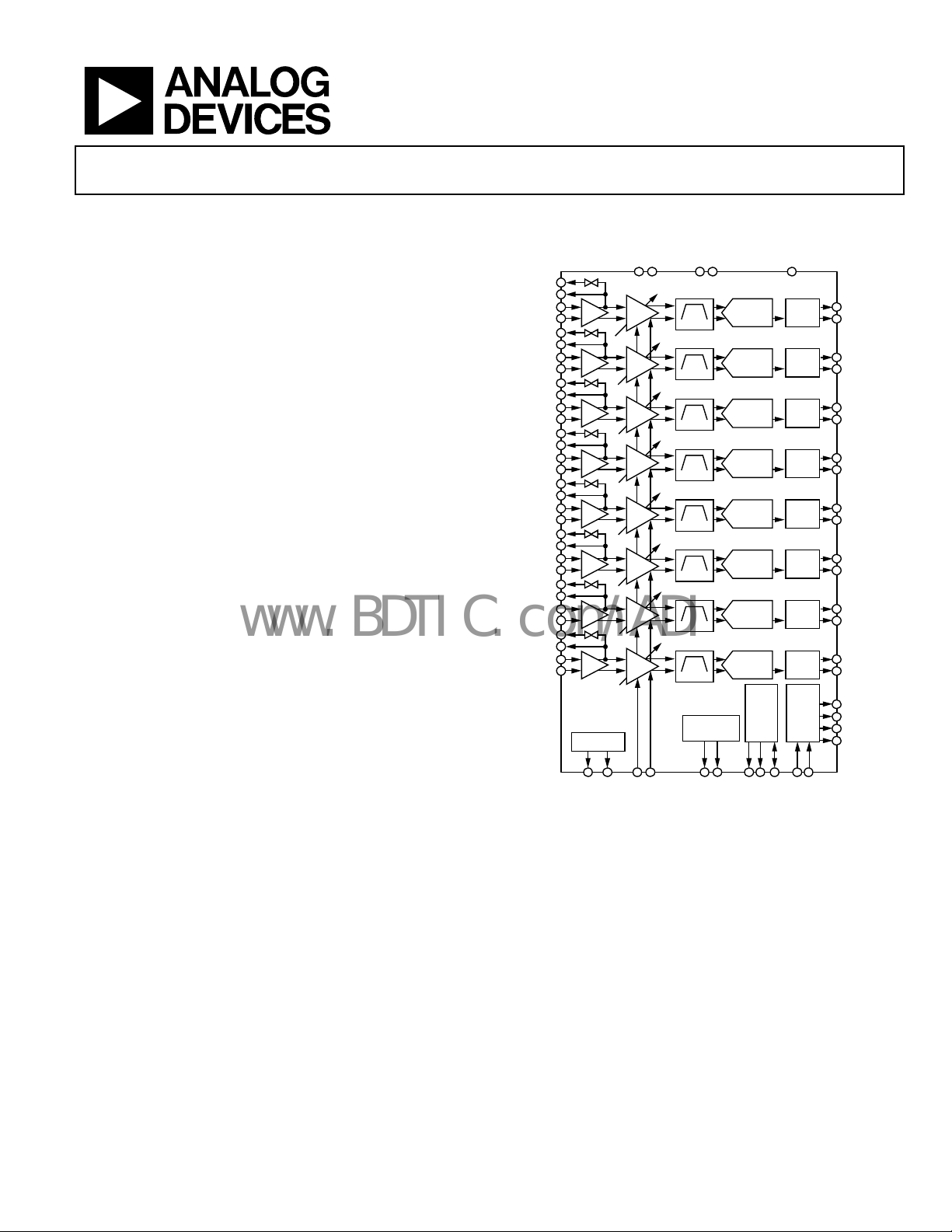
FUNCTIONAL BLOCK DIAGRAM
AVDD1
AVDD2
LNA
LNA
LNA
LNA
LNA
LNA
LNA
LNA
SWITCH
ARRAY
AND
CWD[7:0]+
VGA
VGA
VGA
VGA
VGA
VGA
VGA
VGA
CWD[7:0]–
AAF
AAF
AAF
AAF
AAF
AAF
AAF
AAF
REFERENCE
GAIN–
GAIN+
Figure 1.
PDWN
VREF
STBY
RBIAS
AD9272
12-BIT
ADC
12-BIT
ADC
12-BIT
ADC
12-BIT
ADC
12-BIT
ADC
12-BIT
ADC
12-BIT
ADC
12-BIT
ADC
SERIAL
CSB
AD9272
DRVDD
SERIAL
LVDS
SERIAL
LVDS
SERIAL
LVDS
SERIAL
LVDS
SERIAL
LVDS
SERIAL
LVDS
SERIAL
LVDS
SERIAL
LVDS
RATE
PORT
DATA
INTERFACE
MULTIPLIER
SDIO
CLK–
CLK+
SCLK
DOUTA+
DOUTA–
DOUTB+
DOUTB–
DOUTC+
DOUTC–
DOUTD+
DOUTD–
DOUTE+
DOUTE–
DOUTF+
DOUTF–
DOUTG+
DOUTG–
DOUTH+
DOUTH–
FCO+
FCO–
DCO+
DCO–
07029-001

AD9272
www.BDTIC.com/ADI
NOTES
©2008 Analog Devices, Inc. All rights reserved. Trademarks and
registered trademarks are the property of their respective owners.
D07029F-0-10/08(Sp0)
Rev. Sp0 | Page 2 of 2
 Loading...