

Page 1
Octal LNA/VGA/AAF/ADC
Preliminary Technical Data
FEATURES
8 channels of LNA, VGA, AAF, and ADC
Low noise preamplifier (LNA)
Input-referred noise = 1.2 nV/√Hz @ 7.5 MHz typical
SPI-programmable gain = 14 dB/15.6 dB/18 dB
Single-ended input; V
333 mV p-p/250 mV p-p
Dual mode, active input impedance match
Bandwidth (BW) > 70 MHz
Full-scale (FS) output = 2 V p-p diff
Variable gain amplifier (VGA)
Gain range = −6 dB to +24 dB
Linear-in-dB gain control
Antialiasing filter (AAF)
rd
-order Butterworth cutoff
3
Programmable from 8 MHz to 18 MHz
Analog-to-digital converter (ADC)
12 bits at 10 MSPS to 50 MSPS
SNR = 70 dB
SFDR = 80 dB
Serial LVDS (ANSI-644, IEEE 1596.3 reduced range link)
Data and frame clock outputs
Includes crosspoint switch to support
continuous wave (CW) Doppler
Low power, 150 mW/channel at 12 bits/40 MSPS (TGC)
60 mW/channel in CW Doppler
Single 1.8 V supply (3.3 V supply for CW Doppler output bias)
Flexible power-down modes
Overload recovery in <10 ns
Fast recovery from low power standby mode, <2 μs
100-pin TQFP
APPLICATIONS
Medical imaging/ultrasound
Automotive radar
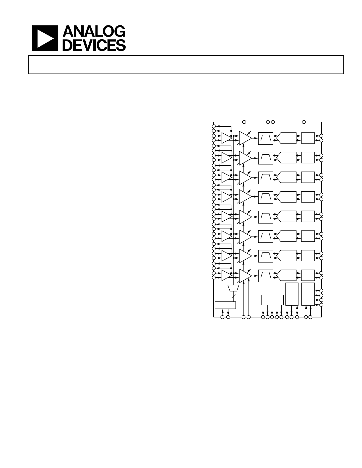
GENERAL DESCRIPTION
The AD9271 is designed for low cost, low power, small size, and
ease of use. It contains eight channels of a variable gain amplifier
(VGA) with low noise preamplifier (LNA); an antialiasing filter
(AAF); and a 12-bit, 10 MSPS to 50 MSPS analog-to-digital
converter (ADC).
maximum = 400 mV p-p/
IN
and Crosspoint Switch
AD9271
The LNA has a single-ended-to-differential gain that is selectable
through the SPI. The LNA input noise is typically 1.2 nV/√Hz,
FUNCTIONAL BLOCK DIAGRAM
LOSW-A
LO-A
LI-A
LG-A
LOSW-B
LO-B
LI-B
LG-B
LOSW-C
LO-C
LI-C
LG-C
LOSW-D
LO-D
LI-D
LG-D
LOSW-E
LO-E
LI-E
LG-E
LOSW-F
LO-F
LI-F
LG-F
LOSW-G
LO-G
LI-G
LG-G
LO-H
LOSW-H
LI-H
LG-H
LNA
LNA
LNA
LNA
LNA
LNA
LNA
LNA
SWITCH
ARRAY
CWVDD
AVDD
VGA
VGA
VGA
VGA
VGA
VGA
VGA
VGA
g
m
6
GAIN–
GAIN+
CWD+/–[5:0]
Figure 1.Block Diagram
STDBY
PWDN
AAF
AAF
AAF
AAF
AAF
AAF
AAF
AAF
REFERENCE
VREF
REFB
SENSE
AD9271
12-BIT
PIPELINE
ADC
12-BIT
PIPELINE
ADC
12-BIT
PIPELINE
ADC
12-BIT
PIPELINE
ADC
12-BIT
PIPELINE
ADC
12-BIT
PIPELINE
ADC
12-BIT
PIPELINE
ADC
12-BIT
PIPELINE
ADC
REFT
RBIAS
DRVDD
CLK +
DOUT + A
DOUT – A
DOUT + B
DOUT – B
DOUT + C
DOUT – C
DOUT + D
DOUT – D
DOUT + E
DOUT – E
DOUT + F
DOUT – F
DOUT + G
DOUT – G
DOUT + H
DOUT – H
FCO+
FCO–
RATE
DCO+
MULTIPLIER
DCO–
CLK –
06304-001
SERIAL
LVDS
SERIAL
LVDS
SERIAL
LVDS
SERIAL
LVDS
SERIAL
LVDS
SERIAL
LVDS
SERIAL
LVDS
SERIAL
LVDS
DATA
PORT
SERIAL
INTERFACE
CSB
SDIO
SCLK
Each channel features a variable gain range of 30 dB, a fully
differential signal path, an active input preamplifier termination, a
maximum gain of up to 40 dB, and an ADC with a conversion
rate of up to 50 MSPS. The channel is optimized for dynamic
performance and low power in applications where a small
package size is critical.
Rev. PrA
Information furnished by Analog Devices is believed to be accurate and reliable. However, no
responsibility is assumed by Anal og Devices for its use, nor for any infringements of patents or ot her
rights of third parties that may result from its use. Specifications subject to change without notice. No
license is granted by implication or otherwise under any patent or patent rights of Analog Devices.
Trademarks and registered trademarks are the property of their respective owners.
and the combined input-referred noise of the entire channel
is 1.4 nV/√Hz at maximum gain. Assuming a 15 MHz noise
bandwidth (NBW) and a 15.6 dB LNA gain, the input SNR is
roughly 86 dB. In CW Doppler mode, the LNA output drives a
transconductance amp that is switched through an 8 × 6,
differential crosspoint switch. The switch is programmable
through the SPI.
One Technology Way, P.O. Box 9106, Norwood, MA 02062-9106, U.S.A.
Tel: 781.329.4700 www.analog.com
Fax: 781.461.3113 ©2007 Analog Devices, Inc. All rights reserved.
Page 2

AD9271 Preliminary Technical Data
TABLE OF CONTENTS
Features.............................................................................................. 1
Input Overdrive.......................................................................... 23
Applications....................................................................................... 1
General Description......................................................................... 1
Functional Block Diagram ..............................................................1
Revision History ...............................................................................2
Product Highlights........................................................................... 3
Specifications..................................................................................... 4
AC Specifications.......................................................................... 4
Digital Specifications ................................................................... 8
Switching Specifications.............................................................. 9
ADC Timing Diagrams .................................................................10
Absolute Maximum Ratings.......................................................... 11
Thermal Impedance................................................................... 11
ESD Caution................................................................................ 11
Pin Configuration and Function Descriptions........................... 12
Equivalent Circuits......................................................................... 15
CW Doppler Operation............................................................. 23
TGC Operation........................................................................... 25
A/D Converter............................................................................ 28
Clock Input Considerations...................................................... 28
Serial Port Interface (SPI).............................................................. 35
Hardware Interface..................................................................... 35
Memory Map .................................................................................. 37
Reading the Memory Map Table.............................................. 37
Reserved Locations .................................................................... 37
Default Values............................................................................. 37
Logic Levels................................................................................. 37
Evaluation Board............................................................................ 42
Power Supplies............................................................................ 42
Input Signals................................................................................ 42
Output Signals ............................................................................42
Typical Performance Characteristics........................................... 17
Theory of Operation ......................................................................20
Ultrasound................................................................................... 20
Channel Overview...................................................................... 21
REVISION HISTORY
x/07—Revision 0: Initial Version
Default Operation and Jumper Selection Settings................. 43
Outline Dimensions....................................................................... 56
Ordering Guide .......................................................................... 56
Rev. PrA | Page 2 of 58
Page 3

Preliminary Technical Data AD9271
The AD9271 requires a LVPECL-/CMOS-/LVDS-compatible
sample rate clock for full performance operation. No external
reference or driver components are required for many
applications.
The ADC automatically multiplies the sample rate clock for
the appropriate LVDS serial data rate. A data clock (DCO) for
capturing data on the output and a frame clock (FCO) trigger
for signaling a new output byte are provided.
Powering down individual channel is supported to increase battery
life for portable applications. There is also a standby mode option
that allows quick power-up for power cycling. In CW Doppler
operation, the VGA, AAF, and ADC are powered down. The
power of the TGC path scales with selectable speed grades.
The ADC contains several features designed to maximize flexibility
and minimize system cost, such as a programmable clock, data
alignment, and programmable digital test pattern generation. The
digital test patterns include built-in fixed patterns, built-in
pseudorandom pattern, and custom user-defined test patterns
entered via the serial port interface.
Fabricated in an advanced CMOS process, the AD9271 is
available in a 14 mm × 14 mm, Pb-free, 100-lead TQFP. It is
specified over the industrial temperature range of –40°C to +85°C.
PRODUCT HIGHLIGHTS
1. Small Footprint. Eight channels are contained in a small,
space-saving package. Full TGC path, ADC, and crosspoint
switch contained within a 100-lead, 16 mm × 16 mm, TQFP.
2. Low power of 150 mW/channel at 40 MSPS.
3. Integrated Crosspoint Switch. This switch allows numerous
multichannel configuration options to enable the CW
Doppler mode.
4. Ease of Use. A data clock output (DCO) operates up to
300 MHz and supports double data rate operation (DDR).
5. User Flexibility. Serial port interface (SPI) control offers a wide
range of flexible features to meet specific system requirements.
6. Integrated Third-Order Antialiasing Filter. This filter is
placed between TGC path and ADC and is programmable
from 8 MHz to 18 MHz.
Rev. PrA | Page 3 of 58
Page 4

AD9271 Preliminary Technical Data
SPECIFICATIONS
AC SPECIFICATIONS
AVDD = 1.8 V, DRVDD = 1.8 V, CWVDD = 3.3 V, 1.0 V internal ADC reference, AIN = 5 MHz, RS = 50 Ω, LNA gain = 15.6 dB (6),
unless otherwise noted.
Table 1.
AD9271-25 AD9271-40 AD9271-50
Parameter1 Conditions Min Typ Max Min Typ Max Min Typ Max Unit
LNA
CHARACTERISTICS
Gain = 5/6/8 Single-ended
Single-ended
Input Voltage
Range, Gain =
5/6/8
Input Common
Mode
Input Resistance RFB = 200 Ω, 50 50 50 Ω
RFB = 400 Ω, 100 100 100 Ω
RFB = ∞ 15 15 15 kΩ
Input Capacitance LI-x 15 15 15 pF
−3 dB Bandwidth 40 60 70 MHz
Input Noise
Voltage,
Gain = 5/6/8
1 dB Input
Compression
Point
Gain = 5/6/8
Active
Termination
Match
Unterminated RFB = ∞ 4.9 4.4 4.2 dB
FULL-CHANNEL (TGC)
CHARACTERISTICS
AAF High-Pass
Cutoff
AAF Low-Pass
Cutoff
Group Delay
Variation
Bandwidth
Tolerance
Input-Referred
Noise Voltage,
LNA Gain =
5/6/8
Correlated Noise No signal −30 −30 −30 dB
Output Offset AAF high-pass
Signal-to-Noise
Ratio (SNR)
FIN = 5 MHz at −7
dBFS
input to
differential
output
input to
single-ended
output
LNA output
limited to
2 V p-p
differential
output
1.4 1.4 1.4 V
R
= 0 Ω, RFB = ∞ 1.4/1.4/1.3 1.3/1.2/1.1 1.3/1.2/1.1 nV/√Hz
S
V
= 0 V 782.6/649.1/508.8 782.6/649.1/508.8 782.6/649.1/508.8 mV p-p
GAIN
Ω, RFB = 200 Ω 6.7 6.7 6.7 dB
−3 dB DC/350/700 DC/350/700 DC/350/700 kHz
−3 dB,
programmable
f = 1 MHz to
10 MHz, gain =
0 V to 1 V
±15 ±15 ±15 %
RFB = ∞ 1.7/1.6/1.5 1.6/1.4/1.3 1.6/1.4/1.2 nV/√Hz
= 700 kHz
GAIN pin = 0 V 65 65 65 dBFS
14/15.6/18 14/15.6/18 14/15.6/18 dB
8/9.6/12 8/9.6/12 8/9.6/12 dB
400/333/250 400/333/250 400/333/250 mV p-p
1/3 × f
(8 to 18)
±1 ±1 ±1 ns
TBD TBD TBD LSB
SAMPLE
1/3 × f
(8 to 18)
SAMPLE
1/3 × f
(8 to 18)
SAMPLE
MHz
2
SE
Rev. PrA | Page 4 of 58
Page 5
Preliminary Technical Data AD9271
AD9271-25 AD9271-40 AD9271-50
Parameter1 Conditions Min Typ Max Min Typ Max Min Typ Max Unit
FIN = 5 MHz at −1
dBFS
Harmonic
Distortion
Second Harmonic,
= 5 MHz at
F
IN
−7 dBFS
Second Harmonic,
= 5 MHz at
F
IN
−1 dBFS
Third Harmonic,
F
= 5 MHz at
IN
−7 dBFS
Third Harmonic,
F
= 5 MHz at
IN
−1 dBFS
Two-Tone IMD3
(2 × F1 − F2)
Distortion
F
= 5.0 MHz at
IN1
−1 dBFS
= 5.1 MHz at
F
IN2
−26 dBFS
Channel-to-
Channel
Crosstalk
Channel-to-
Channel
Crosstalk
(Overrange
Condition)
Overload Recovery LNA or VGA 10 10 10 ns
GAIN ACCURACY
Absolute Gain
Error
0.1 V < V
0.9 V < V
Channel-to-
Channel
Matching
GAIN CONTROL
INTERFACE
Normal Operating
Range
Gain Range 0 V to 1 V 10.6 40.6 10.6 40.6 10.6 40.6 dB
Scale Factor 32 32 32 dB/V
Response Time 30 dB change 350 350 350 ns
CW DOPPLER MODE
Transconductance,
LNA Gain =
5/6/8
Common Mode CW Doppler
Input-Referred
Noise Voltage,
LNA Gain =
5/6/8
Output DC Bias Per channel 2.4 2.4 2.4 mA
Maximum Output
Swing
POWER SUPPLY
AVDD 1.7 1.8 1.9 1.7 1.8 1.9 1.7 1.8 1.9 V
GAIN pin = 1 V 65 65 65 dBFS
GAIN pin = 0 V −65 −65 −65 dBFS
GAIN pin = 1 V −65 −65 −65 dBFS
GAIN pin = 0 V −70 −70 −70 dBFS
GAIN pin = 1 V −70 −70 −70 dBFS
GAIN pin = 1 V −65 −65 −65 dB
−70 −70 −70 dB
−70 −70 −70 dB
3
0 < V
< 0.1 V −1.0 +0.5 +2.0 −1.0 +0.5 +2.0 −1.0 +0.5 +2.0 dB
GAIN
<
GAIN
−1.0 +0.3 +1.0 −1.0 +0.3 +1.0 −1.0 +0.3 +1.0 dB
0.9 V, 1σ
<
GAIN
−2.0 -0.5 +1.0 −2.0 -0.5 +1.0 −2.0 -0.5 +1.0 dB
1 V
0.1 V < V
GAIN
<
1 1 1 dB
0.9 V
0 1 0 1 0 1 V
10/12/16 10/12/16 10/12/16 mA/V
1.5 3.6 1.5 3.6 1.5 3.6 V
output pins
R
= 0 Ω, RFB = ∞ 1.8 /1.7/1.5 1.7 /1.5/1.4 1.7 /1.5/1.3 nV/√Hz
S
Per channel ±2 ±2 ±2 mA p-
Rev. PrA | Page 5 of 58
p
Page 6
AD9271 Preliminary Technical Data
AD9271-25 AD9271-40 AD9271-50
Parameter1 Conditions Min Typ Max Min Typ Max Min Typ Max Unit
DRVDD 1.7 1.8 1.9 1.7 1.8 1.9 1.7 1.8 1.9 V
CWVDD 3.0 3.3 3.6 3.0 3.3 3.6 3.0 3.3 3.6
I
Full-channel
AVDD
CW Doppler
I
49 49 49 mA
DRVDD
Total Power
Dissipation
(Including
Output Drivers)
CW Doppler
Power-Down
Dissipation
Standby Power
Dissipation
Power Supply
Rejection Ratio
(PSRR)
ADC RESOLUTION 12 12 12 Bits
mode
mode with
four channels
enabled
Full-channel
mode
mode with
four channels
enabled
10 mW
65 65 65 mW
1 1 1 mV/V
500 622 746 mA
136 160 170 mA
984 1200 1400 mW
192 216 224 mW
Rev. PrA | Page 6 of 58
Page 7

Preliminary Technical Data AD9271
AD9271-25 AD9271-40 AD9271-50
Parameter1 Conditions Min Typ Max Min Typ Max Min Typ Max Unit
ADC REFERENCE
Output Voltage
Error (VREF = 1
V)
Load Regulation @
1.0 mA (VREF =
1 V)
Input Resistance 6 6 6 kΩ
1
See the AN-835 Application Note, Understanding High Speed ADC Testing and Evaluation, for a complete set of definitions and how these tests were completed.
2
SE = single ended.
3
The overrange condition is specified as being 6 dB more than the full-scale input range.
±2 ±2 ±2 mV
3 3 3 mV
Rev. PrA | Page 7 of 58
Page 8

AD9271 Preliminary Technical Data
DIGITAL SPECIFICATIONS
AVDD = 1.8 V, DRVDD = 1.8 V, CWVDD = 3.3 V, 400 m V p-p differential input, 1.0 V internal ADC reference, AIN = −0.5 dBFS, unless
otherwise noted.
Table 2.
Parameter1 Temperature Min Typ Max Unit
CLOCK INPUTS (CLK+, CLK−)
Logic Compliance CMOS/LVDS/LVPECL
Differential Input Voltage2 Full 250 mV p-p
Input Common-Mode Voltage Full 1.2 V
Input Resistance (Differential) 25°C 20 kΩ
Input Capacitance 25°C 1.5 pF
LOGIC INPUTS (PDWN, STBY, SCLK)
Logic 1 Voltage Full 1.2 3.6 V
Logic 0 Voltage Full 0.3 V
Input Resistance 25°C 30 kΩ
Input Capacitance 25°C 0.5 pF
LOGIC INPUT (CSB)
Logic 1 Voltage Full 1.2 3.6 V
Logic 0 Voltage Full 0.3 V
Input Resistance 25°C 70 kΩ
Input Capacitance 25°C 0.5 pF
LOGIC INPUT (SDIO)
Logic 1 Voltage Full 1.2 DRVDD + 0.3 V
Logic 0 Voltage Full 0 0.3 V
Input Resistance 25°C 30 kΩ
Input Capacitance 25°C 2 pF
LOGIC OUTPUT (SDIO)3
Logic 1 Voltage (IOH = 800 A) Full 1.79 V
Logic 0 Voltage (IOL = 50 A) Full 0.05 V
DIGITAL OUTPUTS (D+, D−), (ANSI-644)1
Logic Compliance LVDS
Differential Output Voltage (VOD) Full 247 454 mV
Output Offset Voltage (VOS) Full 1.125 1.375 V
Output Coding (Default) Offset binary
DIGITAL OUTPUTS (D+, D−),
(Low Power, Reduced Signal Option)
1
Logic Compliance LVDS
Differential Output Voltage (VOD) Full 150 250 mV
Output Offset Voltage (VOS) Full 1.10 1.30 V
Output Coding (Default) Offset binary
1
See the AN-835 Application Note, Understanding High Speed ADC Testing and Evaluation, for a complete set of definitions and how these tests were completed.
2
Specified for LVDS and LVPECL only.
3
Specified for 13 SDIO pins sharing the same connection.
Rev. PrA | Page 8 of 58
Page 9

Preliminary Technical Data AD9271
SWITCHING SPECIFICATIONS
AVDD = 1.8 V, DRVDD = 1.8 V, CWVDD = 3.3 V, 400 m V p-p differential input, 1.0 V internal ADC reference, AIN = −0.5 dBFS, unless
otherwise noted.
Table 3.
Parameter1 Temp Min Typ Max Unit
CLOCK2
Maximum Clock Rate Full 50 MSPS
Minimum Clock Rate Full 10 MSPS
Clock Pulse Width High (tEH) Full 10.0 ns
Clock Pulse Width Low (tEL) Full 10.0 ns
OUTPUT PARAMETERS
Propagation Delay (tPD) Full
Rise Time (tR) (20% to 80%) Full
Fall Time (tF) (20% to 80%) Full
FCO Propagation Delay (t
DCO Propagation Delay (t
DCO to Data Delay (t
DCO to FCO Delay (t
Data-to-Data Skew
DATA-MAX
− t
(t
Wake-Up Time (Standby) 25°C
Wake-Up Time (Power-Down) 25°C
Pipeline Latency Full
APERTURE
Aperture Uncertainty (Jitter) 25°C
1
See the AN-835 Application Note, Understanding High Speed ADC Testing and Evaluation, for a complete set of definitions and how these tests were completed.
2
Can be adjusted via the SPI interface.
3
Measurements were made using a part soldered to FR4 material.
4
t
/24 is based on the number of bits divided by 2, because the delays are based on half duty cycles.
SAMPLE
2, 3
DATA-MIN
) Full
FCO
)4 Full
CPD
)4 Full (t
DATA
)4 Full (t
FRAME
Full
)
1.5 2.3 3.1
300
300
1.5 2.3 3.1
+
t
FCO
/24)
(t
SAMPLE
/24) − 300 (t
SAMPLE
/24) − 300 (t
SAMPLE
±50 ±200
600
375
8
/24) (t
SAMPLE
/24) (t
SAMPLE
ns
/24) + 300 ps
SAMPLE
/24) + 300 ps
SAMPLE
ns
ps
ps
ns
ps
ns
s
CLK
cycles
<1
ps rms
Rev. PrA | Page 9 of 58
Page 10
AD9271 Preliminary Technical Data
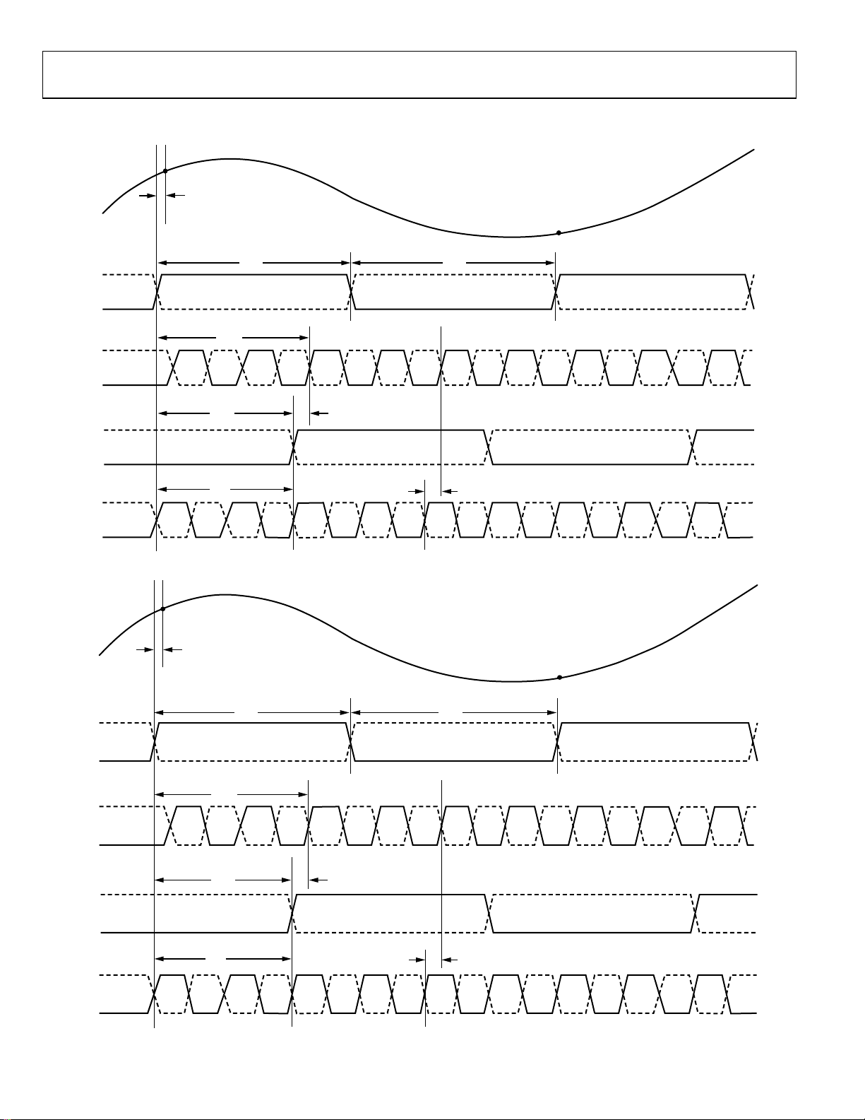
ADC TIMING DIAGRAMS
N – 1
AIN
CLK–
CLK+
DCO–
DCO+
FCO–
FCO+
DOUT–
DOUT+
N – 1
t
A
N
t
FCO
t
t
EH
t
CPD
t
FRAME
PD
MSB
D10
N – 8
N – 8D9N – 8D8N – 8D7N – 8D6N – 8D5N – 8D4N – 8D3N – 8D2N – 8D1N – 8D0N – 8
t
EL
t
DATA
D10
MSB
N – 7
N – 7
6304-002
Figure 2. 12-(Preliminary) Bit Data Serial Stream (Default)
AIN
CLK–
CLK+
DCO–
DCO+
FCO–
FCO+
DOUT–
DOUT+
t
A
N
t
EH
t
CPD
t
FCO
t
PD
t
FRAME
LSB
(N – 8)D0(N – 8)D1(N – 8)D2(N – 8)D3(N – 8)D4(N – 8)D5(N – 8)D6(N – 8)D7(N – 8)D8(N – 8)D9(N – 8)
t
EL
t
DATA
D10
(N – 8)
LSB
(N – 7)
D0
(N – 7)
06304-004
Figure 3. 12-(Preliminary) Bit Data Serial Stream, LSB First
Rev. PrA | Page 10 of 58
Page 11
Preliminary Technical Data AD9271
ABSOLUTE MAXIMUM RATINGS
Table 4.
With
Parameter
Respect To Rating
ELECTRICAL
AVDD GND −0.3 V to +2.0 V
DRVDD GND −0.3 V to +2.0 V
CWVDD GND −0.3 V to +3.9 V
GND GND −0.3 V to +0.3 V
AVDD DRVDD −2.0 V to +2.0 V
Digital Outputs
GND −0.3 V to +2.0 V
(DOUT+, DOUT−, DCO+,
DCO−, FCO+, FCO−)
CLK+, CLK− GND −0.3 V to +3.9 V
LI-x LG-x −0.3 V to +2.0 V
LO-x LG-x −0.3 V to +2.0 V
LOSW-x LG-x −0.3 V to +2.0 V
CWDx−, CWDx+ GND −0.3 V to +2.0 V
SDIO, GAIN+,GAIN− GND −0.3 V to +2.0 V
PDWN, STBY, SCLK, CSB GND −0.3 V to +3.9 V
REFT, REFB, RBIAS GND −0.3 V to +2.0 V
VREF, SENSE GND −0.3 V to +2.0 V
ENVIRONMENTAL
Operating Temperature
−40°C to +85°C
Range (Ambient)
Maximum Junction
150°C
Temperature
Lead Temperature
300°C
(Soldering, 10 sec)
Storage Temperature
−65°C to +150°C
Range (Ambient)
Stresses above those listed under Absolute Maximum Ratings
may cause permanent damage to the device. This is a stress
rating only; functional operation of the device at these or any
other conditions above those indicated in the operational
section of this specification is not implied. Exposure to absolute
maximum rating conditions for extended periods may affect
device reliability.
THERMAL IMPEDANCE
Table 5.
Air Flow Velocity (m/s) θ
0.0 20.3°C/W
1.0 14.4°C/W 7.6°C/W 4.7°C/W
2.5 12.9°C/W
1
θ
for a 4-layer PCB with solid ground plane (simulated). Exposed pad
JA
soldered to PCB.
1
θ
JA
JB
θJC
ESD CAUTION
Rev. PrA | Page 11 of 58
Page 12
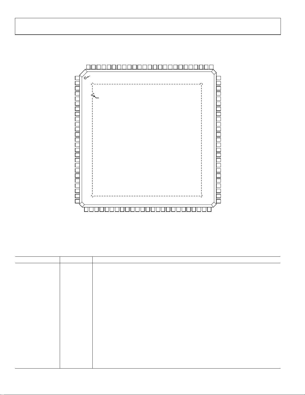
AD9271 Preliminary Technical Data
G
PIN CONFIGURATION AND FUNCTION DESCRIPTIONS
LOSW-D
LO–D
CWD0–
CWD0+
CWD1–
CWD1+
CWD2–
CWD2+
CWVD-D
GAIN–
GAIN+
RBIAS
SENSE
VREF
REFB
REFT
AVDD
CWD3–
CWD3+
CWD4–
CWD4+
CWD5–
CWD5+
LO–E
LOSW-E
LI-E
LG-E
AVDD
AVDD
LO-F
LOSW-F
LI-F
LG-F
AVDD
AVDD
LO-G
LOSW-
LI-G
LG-G
AVDD
AVDD
LO-H
LOSW-H
LI-H
LG-H
AVDD
AVDD
CLK–
CLK+
AVDD
9998979695949392919089888786858483828180797877
100
PIN 1
1
INDICATOR
2
3
4
5
6
7
8
9
10
11
12
13
14
15
16
17
18
19
20
21
22
23
24
25
EXPOSED PADDLE, PIN 0
(BOTTOM OF PACKAGE)
AD9271
TOP VIEW
(Not to Scale)
76
LI-D
75
LG-D
74
AVDD
73
AVDD
72
LO-C
71
LOSW-C
70
LI-C
69
LG-C
68
AVDD
67
AVDD
66
LO-B
65
64
LOSW-B
LI-B
63
LG-B
62
AVDD
61
AVDD
60
59
LO-A
58
LOSW-A
57
LI-A
LG-A
56
AVDD
55
54
AVDD
53
CSB
52
SDIO
SCLK
51
2627282930313233343536373839404142434445464748
FCO–
DRVDD
DCO–
DOUT + F
DOUT – H
DOUT + H
DOUT – G
DOUT + G
DOUT – F
DOUT – E
DOUT + E
FCO+
DCO+
DOUT – B
DOUT – C
DOUT – D
DOUT + D
DOUT + B
DOUT + C
DRVDD
DOUT – A
DOUT + A
50
49
STBY
AVDD
PWDN
Figure 4. 100-Lead TQFP
Table 6. Pin Function Descriptions
Pin No. Name Description
0 GND Ground (Exposed paddle should be tied to a quiet analog ground)
3, 4, 9, 10, 15,
AVDD 1.8 V Analog Supply
16, 21, 22, 25,
50, 54, 55, 60,
61, 66, 67, 72,
73,92
26, 47 DRVDD 1.8 V Digital Output Driver Supply
84 CWVDD 3.3 V Analog Supply
1 LI-E LNA Analog Input for Channel E
2 LG-E LNA Ground for Channel E
5 LO-F LNA Analog Output for Channel F
6 LOSW-F LNA Analog Output Complement for Channel F
7 LI-F LNA Analog Input for Channel F
8 LG-F LNA Ground for Channel F
11 LO-G LNA Analog Output for Channel G
12 LOSW-G LNA Analog Output Complement for Channel G
13 LI-G LNA Analog Input for Channel G
14 LG-G LNA Ground for Channel G
06304-005
Rev. PrA | Page 12 of 58
Page 13

Preliminary Technical Data AD9271
Pin No. Name Description
17 LO-H LNA Analog Output for Channel H
18 LOSW-H LNA Analog Output Complement for Channel H
19 LI-H LNA Analog Input for Channel H
20 LG-H LNA Ground for Channel H
23 CLK− Clock Input Complement
24 CLK+ Clock Input True
27 DOUT − H ADC H Digital Output Complement
28 DOUT + H ADC H True Digital Output True
29 DOUT − G ADC C Digital Output Complement
30 DOUT + G ADC C True Digital Output
31 DOUT − F ADC B Digital Output Complement
32 DOUT + F ADC B True Digital Output True
33 DOUT − E ADC A Digital Output Complement
34 DOUT + E ADC A True Digital Output True
35 DCO− Frame Clock Digital Output Complement
36 DCO+ Frame Clock Digital Output True
37 FCO− Frame Clock Digital Output Complement
38 FCO+ Frame Clock Digital Output True
39 DOUT − D ADC H Digital Output Complement
40 DOUT + D ADC H True Digital Output True
41 DOUT − C ADC C Digital Output Complement
42 DOUT + C ADC C True Digital Output
43 DOUT − B ADC B Digital Output Complement
44 DOUT + B ADC B True Digital Output True
45 DOUT − A ADC A Digital Output Complement
46 DOUT + A ADC A True Digital Output True
48 STDBY Standby Power Down
49 PDWN Full Power Down
51 SCLK Serial Clock
52 SDIO Serial Data Input/Output
53 CSB Chip Select Bar
56 LG-A LNA Ground for Channel A
57 LI-A LNA Analog Input for Channel A
58 LOSW-A LNA Analog Output Complement for Channel A
59 LO-A LNA Analog Output for Channel A
62 LG-B LNA Ground for Channel B
63 LI-B LNA Analog Input for Channel B
64 LOSW-B LNA Analog Output Complement for Channel B
65 LO-B LNA Analog Output for Channel B
68 LG-C LNA Ground for Channel C
69 LI-C LNA Analog Input for Channel C
70 LOSW-C LNA Analog Output Complement for Channel C
71 LO-C LNA Analog Output for Channel C
74 LG-D LNA Ground for Channel D
75 LI-D LNA Analog Input for Channel D
76 LOSW-D LNA Analog Output Complement for Channel D
77 LO-D LNA Analog Output for Channel D
78 CWD0− CW Doppler Output Complement for Channel 0
79 CWD0+ CW Doppler Output True for Channel 0
80 CWD1− CW Doppler Output Complement for Channel 1
81 CWD1+ CW Doppler Output True for Channel 1
82 CWD2− CW Doppler Output Complement for Channel 2
83 CWD2+ CW Doppler Output True for Channel 2
Rev. PrA | Page 13 of 58
Page 14

AD9271 Preliminary Technical Data
Pin No. Name Description
85 GAIN− GAIN Control Voltage Input Complement
86 GAIN+ GAIN Control Voltage Input True
87 RBIAS External resistor sets the internal ADC core bias current
88 SENSE Reference Mode Selection
89 VREF Voltage Reference Input/Output
90 REFB Differential Reference (Negative)
91 REFT Differential Reference (Positive)
93 CWD3− CW Doppler Output Complement for Channel 3
93 CWD3+ CW Doppler Output True for Channel 3
95 CWD4− CW Doppler Output Complement for Channel 4
96 CWD4+ CW Doppler Output True for Channel 4
97 CWD5− CW Doppler Output Complement for Channel 5
98 CWD5+ CW Doppler Output True for Channel 5
99 LO-E LNA Analog Output for Channel E
100 LOSW-E LNA Analog Output Complement for Channel E
Rev. PrA | Page 14 of 58
Page 15
Preliminary Technical Data AD9271
V
Ω
A
S
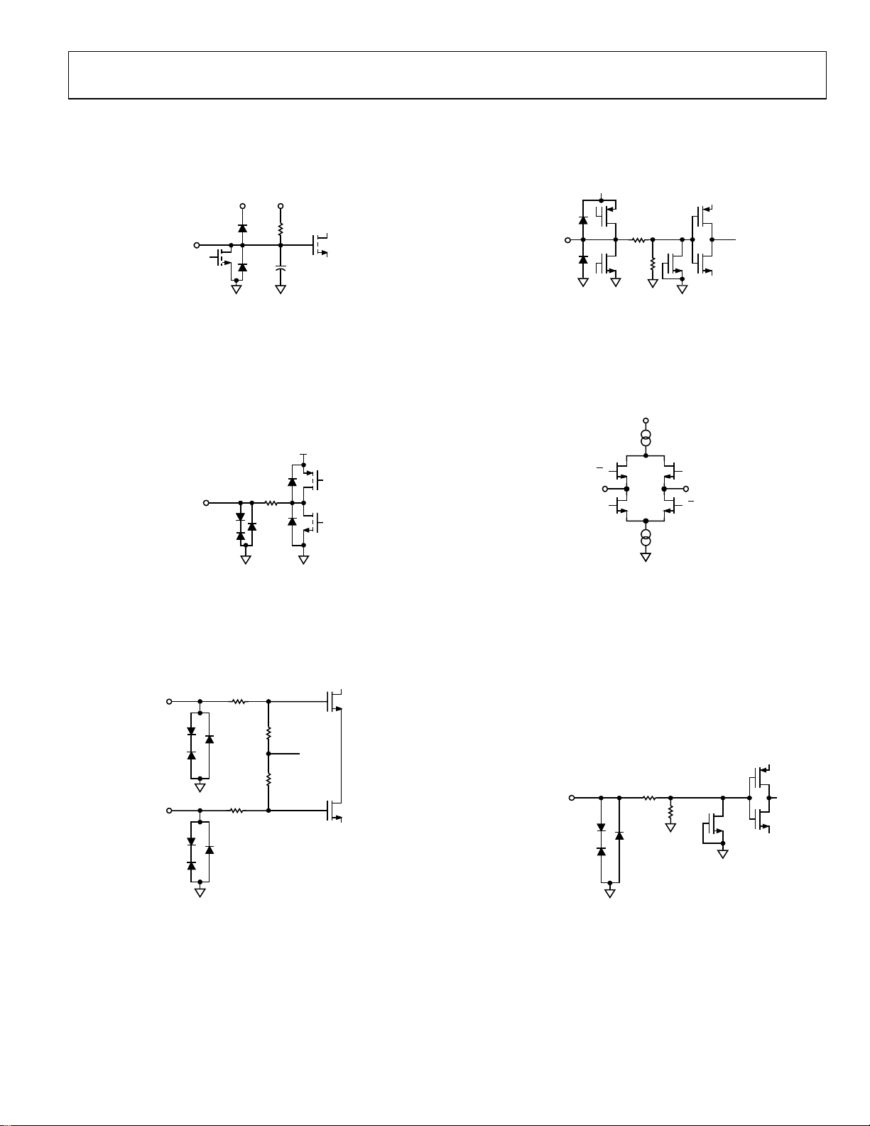
EQUIVALENT CIRCUITS
CM
15kΩ
06304-073
LI-x,
LG-x
AVDD
Figure 5. Equivalent LNA Input Circuit
AVDD
LO-x,
LOSW-x
10Ω
Figure 6. Equivalent LNA Output Circuit
VDD
SDIO
350Ω
30kΩ
06304-008
Figure 8. Equivalent SDIO Input Circuit
DRVDD
V
DOUT– DOUT+
V
06304-075
DRGND
V
V
6304-009
Figure 9. Equivalent Digital Output Circuit
CLK+
CLK–
10
10kΩ
10kΩ
10Ω
Figure 7. Equivalent Clock Input Circuit
1.25V
06304-007
Rev. PrA | Page 15 of 58
CLK OR PDWN
OR STBY
1kΩ
30kΩ
Figure 10. Equivalent SCLK Input Circuit
06304-010
Page 16
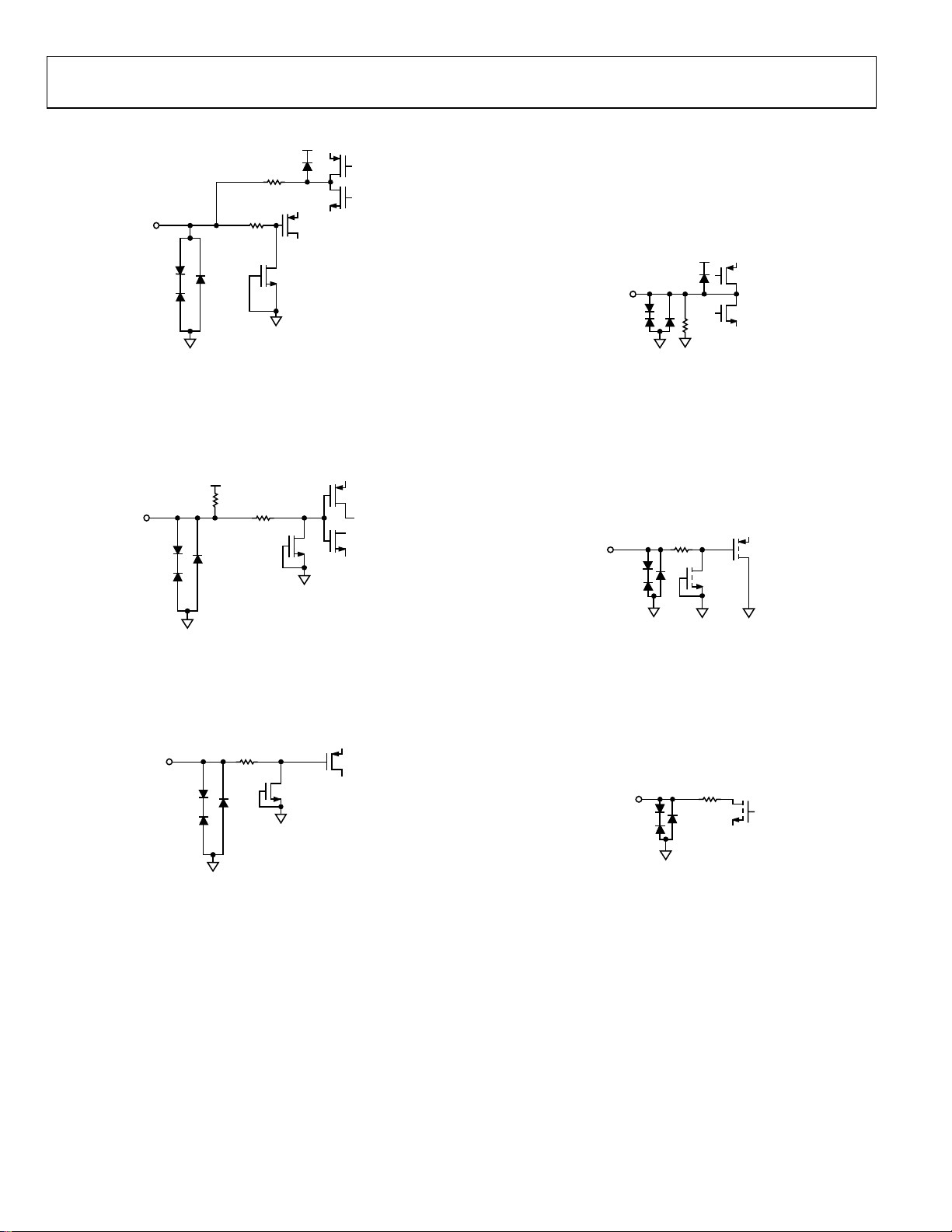
AD9271 Preliminary Technical Data
A
V
C
Ω
AVDD
RBIAS
100Ω
Figure 11. Equivalent RBIAS Circuit
DD
70kΩ
CSB
1kΩ
Figure 12. Equivalent CSB Input Circuit
AVDD
VREF
6kΩ
06304-011
6304-014
Figure 14. Equivalent VREF Circuit
GAIN
06304-012
50Ω
06304-074
Figure 15. Equivalent GAIN Input Circuit
SENSE
Figure 13. Equivalent SENSE Circuit
1kΩ
WDx+,
CWDx–
06304-013
10
06304-076
Figure 16. Equivalent CWD Output Circuit
Rev. PrA | Page 16 of 58
Page 17
Preliminary Technical Data AD9271
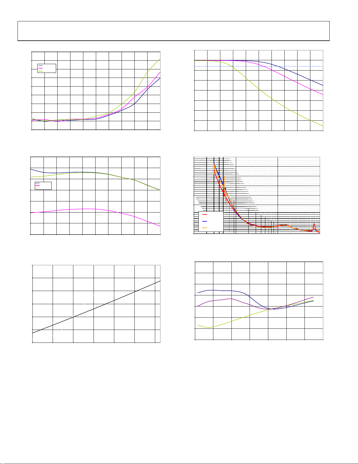
TYPICAL PERFORMANCE CHARACTERISTICS
(f
= 50 MSPS, AIN = 5 MHz, LPF = 1/3 × f
SAMPLE
, LNA gain = 6×)
SAMPLE
2.00
1.50
1.00
0.50
0.00
Absolute Error (dB)
-0.50
-1.00
-1.50
-2.00
0 0.1 0.2 0.3 0.4 0.5 0.6 0.7 0.8 0.9 1
Figure 17. Absolute Gain Error vs. V
85C
25C
-40C
Vgain (V)
at Three Temperatures
GAIN
2000000
1800000
1600000
1400000
1200000
1000000
Number of Hits
800000
600000
400000
200000
0
-5-4-3-2-1012345
Figure 20. Output-Referred Noise Histogram with Gain Pin at 0.0V, AD9271-
Codes
50
1200000
1000000
800000
600000
Number of Hits
400000
Figure 18. Gain Error Histogram
Figure 19. Gain Match Histogram for V
= 0.2 V and 0.7 V
GAIN
200000
0
-5-4-3-2-1012345
Codes
Figure 21. Output-Referred Noise Histogram with Gain Pin at 1.0V, AD9271-
50
4.5
4
3.5
3
2.5
2
Input-referred Noise (nV/sqrt-Hz )
1.5
1
0.5
0
0 5 10 15 20 25
LNA Gain = 5x
LNA Gain = 6x
LNA Gain = 8x
Frequency (MHz)
Figure 22. Short-Circuit, Input-Referred Noise vs. Frequency
Rev. PrA | Page 17 of 58
Page 18
AD9271 Preliminary Technical Data
-99
-100
LNA Gain = 5x
LNA Gain = 6x
-101
LNA Gain = 8x
-102
-103
-104
-105
Output-referred Noise (d BFS/rt-Hz)
-106
-107
-108
0 0.1 0.2 0.3 0.4 0.5 0.6 0.7 0.8 0.9 1
Figure 23. Short-Circuit, Output-Referred Noise vs. V
66
64
62
SNR (dBFS)
SINAD (dB)
SINAD (dBFS)
60
SNR/SINAD
58
56
54
52
0 0.1 0.2 0.3 0.4 0.5 0.6 0.7 0.8 0.9 1
Vgain (V)
GAIN
Vgain (V)
Figure 24. SNR/SINAD vs. Gain
1.7
1.65
1.6
1.55
0
-5
-3dB line
-10
-15
-20
Fundamental (dBFS)
-25
-30
-35
-40
0 2.5 5 7.5 10 12.5 15 17.5 20 22.5 25
Figure 26. Antialiasing Filter (AAF) Pass-Band Response
400
350
300
250
200
Group Delay (ns)
150
100
Vgain = 0.0 V
Vgain = 0.5 V
50
Vgain = 1.0 V
0
0.1 1 10 100
Frequency (MHz)
Analog Input Frequency (MHz)
(1/3)*25MHz
(1/3)*50MHz
(1/3)*40MHz
Figure 27. Antialiasing Filter (AAF) Group Delay Response
-50
-55
-60
-65
H2 (dBFS)
-70
Vgain=0.2V
Vgain=1V
1.5
Input-referred noise (nV/rt-Hz)
1.45
1.4
-40-200 20406080
Temperature (C)
Figure 25. Short-Circuit, Input-Referred Noise vs. Temperature
Rev. PrA | Page 18 of 58
-75
-80
-85
2 4 6 8 10 12 14 16
Vgain=0.5V
Fin (MHz)
Figure 28. Second-Order Harmonic Distortion vs. Frequency
Page 19

Preliminary Technical Data AD9271
-50
-40
-55
-60
-65
Vgain=1V
H3 (dBFS)
-70
-75
Vgain=0.2V
-80
-85
2 4 6 8 10121416
Figure 29. Third-Order Harmonic Distortion vs. Frequency
-40
-50
-60
Vgain=0V
Vgain=0.5V
Vgain=1V
-70
-80
Second Harmonic (dBFS)
-90
-100
-110
-40 -35 -30 -25 -20 -15 -10 -5 0
Vgain=0.5V
Fin (MHz)
ADC Output Level (dBFS)
Figure 30. Second-Order Harmonic Distortion vs. ADC Output Level
-50
-60
Vgain=0V
Vgain=0.5V
Vgain=1V
-70
-80
Third Harmonic (dBFS)
-90
-100
-110
-40 -35 -30 -25 -20 -15 -10 -5 0
ADC Output Level (dBFS)
Figure 31. Third-Order Harmonic Distortion vs. ADC Output Level
Rev. PrA | Page 19 of 58
Page 20

AD9271 Preliminary Technical Data
THEORY OF OPERATION
ULTRASOUND
The primary application for the AD9271 is medical ultrasound.
Figure 32 shows a simplified block diagram of an ultrasound
system. A critical function of an ultrasound system is the time
gain control (TGC) compensation for physiological signal
attenuation. Because the attenuation of ultrasound signals is
exponential with respect to distance (time), a linear-in-dB VGA
is the optimal solution.
Key requirements in an ultrasound signal chain are very low
noise, active input termination, fast overload recovery, low
power, and differential drive to an ADC. Because ultrasound
machines use beam-forming techniques requiring large binaryweighted numbers (for example, 32 to 512) of channels, the
lowest power at the lowest possible noise is of key importance.
TX HV AMPs
Most modern machines use digital beam forming. In this
technique, the signal is converted to digital format immediately
following the TGC amplifier; beam forming is done digitally.
The ADC resolution of 12 bits with up to 50 MSPS sampling
satisfies the requirements of both general-purpose and highend systems.
Power consumption and low cost are of primary importance in
low-end and portable ultrasound machines, and the AD9271 is
designed for these criteria.
For additional information regarding ultrasound systems, refer
to “How Ultrasound System Considerations Influence Front-End
Component Choice,” Analog Dialogue, Volume 36, Number 3,
May–July 2002.
TX BEAMFORMER
BEAMFORMER
CENTRAL CONT ROL
MULTICHANNEL
TGC USES MANY VG As
AD9271
TRANSDUCER
ARRAY
128, 256 ETC.
ELEMENTS
HV
MUX/
DEMUX
BIDIRECTIO NAL
CABLE
T/R
SWITCHES
TIME GAIN COMPENSATION
TGC
VGALNA
CW
CW (ANALOG)
BEAMFORMER
AUDIO
OUTPUT
Figure 32. Simplified Ultrasound System Block Diagram
AAF
ADC
SPECTRAL
DOPPLER
PROCESSING
MODE
Rx BEAMFORMER
(B AND F MODES)
IMAGE AND
MOTION
PROCESSING
(B MODE)
DISPLAY
COLOR
DOPPLER (PW )
PROCESSING
(F MODE)
06304-077
Rev. PrA | Page 20 of 58
Page 21

Preliminary Technical Data AD9271
RFB1
CFB
RFB2
LO-X
LOSW-X
g
m
TO
SWITCH
ARRAY
CDW+
CDW–
CS
CSH
RS
CLG
LI-X
LG-X
LNA
ATTENUATOR
–30dB TO 0d B
GAIN
INTERPOL ATOR
Figure 33. Simplified Block Diagram of Single Channel
CHANNEL OVERVIEW
Each channel contains both a TGC and CW Doppler signal
path. Common to both signal paths, the LNA provides useradjustable input impedance termination. The CW Doppler path
includes a transconductance amplifier and crosspoint switch.
The TGC path includes a differential X-AMP® VGA, an
antialiasing filter, and an ADC. Figure 33 shows a simplified
block diagram with external components.
The signal path is fully differential throughout to maximize
signal swing and reduce even-order distortion; however, the
LNA is designed to be driven from a single-ended signal source.
Low Noise Amplifier (LNA)
Good noise performance relies on a proprietary ultralow noise
LNA at the beginning of the signal chain, which minimizes the
noise contribution in the following VGA. Active impedance
control optimizes noise performance for applications that benefit
from input impedance matching.
A simplified schematic of the LNA is shown in Figure 34. LI-x is
capacitively coupled to the source. An on-chip bias generator
establishes dc input bias voltages of around 1.4 V and centers
the output common-mode levels at 0.9 V (VDD/2). A capacitor,
C
, of the same value as the input coupling capacitor, CS, is
LG
connected from the LG-x pin to ground.
CFB
RFB1
RFB2
LOSW
LO-X
CS
RS
CSH
LI-X
LG-X
CLG
+24dB
GAIN–
GAIN+
AAF
SERIAL PORT
INTERFACE
CSB
12-BIT
PIPELINE
ADC
SDIO
SCLK
SERIAL
LVDS
AD9271
DOUT + X
DOUT – X
06304-071
The LNA supports differential output voltages as high as 2 V p-p
with positive and negative excursions of ±0.5 V from a
common-mode voltage of 0.9 V. The LNA differential gain sets
the maximum input signal before saturation. One of three gains
is set through the SPI. The corresponding input full-scale for
the gain settings of 5, 6, or 8 is 400 mV p-p, 333 mV p-p, and
250 mV p-p, respectively. Overload protection ensures quick
recovery time from large input voltages. Because the inputs are
capacitively coupled to a bias voltage near midsupply, very large
inputs can be handled without interacting with the ESD protection.
Low value feedback resistors and the current-driving capability
of the output stage allow the LNA to achieve a low input-referred
noise voltage of 1.2 nV/√Hz. This is achieved with a current
consumption of only 16 mA per channel (30 mW). On-chip
resistor matching results in precise single-ended gains critical
for accurate impedance control. The use of a fully differential
topology and negative feedback minimizes distortion. Low HD2
is particularly important in second harmonic ultrasound imaging
applications. Differential signaling enables smaller swings at
each output, further reducing third-order distortion.
Active Impedance Matching
The LNA consists of a single-ended voltage gain amplifier with
differential outputs and the negative output externally available.
For example, with a fixed gain of 6 (15.6 dB), an active input
termination is synthesized by connecting a feedback resistor
between the negative output pin, LO-x, and the positive input
pin, LI-x. This technique is well known and results in the input
resistance shown in Equation 2, where A/2 is the single-ended
gain or the gain from the LI-x inputs to the LO-x outputs.
R
FB
R
=
IN
1(
(2)
A
)
+
2
Figure 34. Simplified LNA Schematic
06304-101
Rev. PrA | Page 21 of 58
Page 22

AD9271 Preliminary Technical Data
is needed in series with RFB because the dc levels at Pin LO-x
C
Because the amplifier has a gain of 6× from its input to its
differential output, it is important to note that the gain A/2 is
the gain from Pin LI-x to Pin LO-x, and is 6 dB less than the
gain of the amplifier, or 9.6 dB (3×). The input resistance is
reduced by an internal bias resistor of 15 kΩ in parallel with the
source resistance connected to Pin LI-x, with Pin LG-x ac
IN
, the
FB
grounded. Equation 3 can be used to calculate the needed R
for a desired R
R
IN
For example, to set R
, even for higher values of RIN.
IN
R
FB
= k15||
+
)31(
(3)
Ω
to 200 Ω, the value of RFB is 845 Ω. If the
IN
simplified equation, Equation 2, is used to calculate R
resulting value is 190 Ω, resulting in a less than 0.1 dB gain
error. Factors such as a dynamic source resistance might
influence the absolute gain accuracy more significantly. At
higher frequencies, the input capacitance of the LNA needs to
be considered. The user must determine the level of matching
accuracy and adjust R
accordingly.
FB
The bandwidth (BW) of the LNA is about 70 MHz. Ultimately
the BW of the LNA limits the accuracy of the synthesized R
= RS up to about 200 Ω, the best match is between
For R
IN
.
IN
100 kHz and 10 MHz, where the lower frequency limit is
determined by the size of the ac-coupling capacitors, and the
upper limit, by the LNA BW. Furthermore, the input
capacitance and R
1k
RIN = 500Ω, RFB = 2.5kΩ
RIN = 200Ω, RFB = 1kΩ
100
RIN = 100Ω, RFB = 499Ω
limit the BW at higher frequencies.
S
RSH = ∞, CSH = 0 pF
RSH = 50Ω, CSH = 22 pF
FB
and Pin LI-x are unequal.
Table 7. Active Termination External Component Values
Minimum
LNA Gain RIN (Ω) RFB (Ω)
CSH (pF) BW (MHz)
5× 50 175 90 49
6× 50 200 70 59
8× 50 250 50 73
5× 100 350 30 49
6× 100 400 20 59
8× 100 500 10 73
5× 200 700 na 49
6× 200 800 na 49
8× 200 1000 na 49
LNA Noise
The short-circuit noise voltage (input-referred noise) is an
important limit on system performance. The short-circuit noise
voltage for the LNA is 1.2 nV/√Hz or 1.4 nV/√Hz (at maximum
gain), including the VGA noise. These measurements, which
are taken without a feedback resistor, provide the basis for
calculating the input noise and noise figure performance of the
configurations shown in Figure 43. Figure 43 and Figure 44 are
simulations of noise figure vs. R
results using these
S
configurations and an input-referred noise voltage for the VGA
of 4 nV/√Hz. Unterminated (R
= ∞) operation exhibits the
FB
lowest equivalent input noise and noise figure. Figure 44 shows
the noise figure vs. source resistance rising at low R
—where the
S
LNA voltage noise is large compared with the source noise—
and at high R
due to current noise.
S
UNTERMINATED
R
IN
R
S
+
V
IN
–
V
OUT
INPUT IMPEDANCE (Ω)
10
RIN = 50Ω, RFB = 249Ω
1M100k 50M10M
FREQUENCY (Hz)
RSH = ∞, CSH = 0 pF
RSH = 50Ω, CSH = 22 pF
Figure 35. RIN vs. Frequency for Various Values of RFB
(Effects of R
and CSH are Also Shown
SH
Figure 35 shows RIN vs. frequency for various values of RFB. Note
that at the lowest value, 50 Ω, R
peaks at frequencies greater
IN
than 10 MHz. This is due to the BW roll-off of the LNA as
mentioned earlier.
However, as can be seen for larger R
values, parasitic capacitance
IN
starts rolling off the signal BW before the LNA can produce
peaking. C
not be used for values of R
lists the recommended values for R
further degrades the match; therefore, CSH should
SH
that are greater than 100 Ω. Table 7
IN
and CSH in terms of RIN.
FB
Rev. PrA | Page 22 of 58
RESISTIVE TERMINAT ION
R
IN
R
S
+
V
IN
–
ACTIVE IMPEDANCE MATCH
R
S
+
V
IN
–
RIN=
R
IN
1 + A/2
R
S
R
FB
Figure 36. Input Configurations
V
OUT
R
FB
V
OUT
03199-079
Page 23

Preliminary Technical Data AD9271
V
7
INCLUDES NOISE OF VGA
6
5
4
3
NOISE FI GURE (dB)
2
1
SIMULATION
0
50 100 1k
RESISTIVE TERMINAT ION
Figure 37. Noise Figure vs. R
= RIN)
(R
S
ACTIVE IM PEDANCE MATCH
UNTERMINATED
RS (Ω)
for Resistive,
S
03199-076
Active Matched and Unterminated Inputs, Gain = 1 V
7
INCLUDES NOISE OF VGA
6
5
4
3
NOISE FI GURE (dB)
2
1
SIMULATION
0
50 100 1k
Figure 38. Noise Figure vs. R
R
R
R
= 50Ω
IN
R
= 75Ω
IN
= 100Ω
IN
= 200Ω
IN
R
=
∞
FB
RS (Ω)
for Various Fixed Values of RIN,
S
03199-077
Actively Matched, Gain = 1 V.
The primary purpose of input impedance matching is to
improve the system transient response. With resistive termination,
the input noise increases due to the thermal noise of the
matching resistor and the increased contribution of the LNA’s
input voltage noise generator. With active impedance matching,
however, the contributions of both are smaller than they would
be for resistive termination by a factor of 1/(1 + LNA Gain).
Figure 37 shows the relative noise figure (NF) performance. In
this graph, the input impedance was swept with R
to preserve
S
the match at each point. The noise figures for a source impedance
of 50 are 7.1 dB, 4.1 dB, and 2.5 dB for the resistive, active,
and unterminated configurations, respectively. The noise
figures for 200 are 4.6 dB, 2.0 dB, and 1.0 dB, respectively.
Figure 38 shows the NF vs. R
for various values of RIN, which is
S
helpful for design purposes. The plateau in the NF for actively
matched inputs mitigates source impedance variations. For
comparison purposes, a preamp with a gain of 15.6 dB and
noise spectral density of 1.2 nV/√Hz, combined with a VGA
with 4 nV/√Hz, yields a noise figure degradation of
approximately 1.5 dB (for most input impedances), which is
significantly worse than the AD9271 performance.
Rev. PrA | Page 23 of 58
INPUT OVERDRIVE
Excellent overload behavior is of primary importance in ultrasound. Both the LNA and VGA have built-in overdrive
protection and quickly recover after an overload event.
Input Overload Protection
As with any amplifier, voltage clamping prior to the inputs is
highly recommended if the application is subject to high
transient voltages.
A block diagram of a simplified ultrasound transducer interface
is shown in Figure 39. A common transducer element serves the
dual functions of transmitting and receiving ultrasound energy.
During the transmitting phase, high voltage pulses are applied
to the ceramic elements. A typical transmit/receive (T/R) switch
may consist of four high voltage diodes in a bridge configuration.
Although the diodes ideally block transmit pulses from the
sensitive receiver input, diode characteristics are not ideal, and
resulting leakage transients imposed on the LI-x inputs can be
problematic.
Because ultrasound is a pulse system and time-of-flight is used
to determine depth, quick recovery from input overloads is
essential. Overload can occur in the preamp and the VGA.
Immediately following a transmit pulse, the typical VGA gains
are low, and the LNA is subject to overload from T/R switch
leakage. With increasing gain, the VGA can become overloaded
due to strong echoes that occur near field echoes and
acoustically dense materials, such as bone.
Figure 39 illustrates an external overload protection scheme. A
pair of back-to-back Schottky diodes is installed prior to
installing the ac-coupling capacitors. Although the BAS40
diodes are shown, any diode is prone to exhibiting some amount
of shot noise. Many types of diodes are available for achieving the
desired noise performance. The configuration shown in Figure
39 tends to add 2 nV√Hz of input-referred noise. Decreasing the
5 kΩ resistor and increasing the 2 kΩ resistor may improve noise
contribution, depending on the application. With the diodes
shown in Figure 39, clamping levels of ±0.5 V or less
significantly enhances the system overload performance.
+5
Tx
DRIVER
TRANSDUCER
5kΩ
5kΩ
HV
BAS40-04
2kΩ
–5V
10nF
10nF
Figure 39. Input Overload Protection
AD9271
LNA
6304-100
CW DOPPLER OPERATION
Modern ultrasound machines used for medical applications
employ a 2
n
binary array of receivers for beam forming, with
Page 24

AD9271 Preliminary Technical Data
typical array sizes of 16 or 32 receiver channels phase-shifted
and summed together to extract coherent information. When
used in multiples, the desired signals from each of the channels
can be summed to yield a larger signal (increased by a factor N,
where N is the number of channels), and the noise is increased by
the square root of the number of channels. This technique
enhances the signal-to-noise performance of the machine. The
critical elements in a beam-former design are the means to
align the incoming signals in the time domain and the means to
sum the individual signals into a composite whole.
Beam forming, as applied to medical ultrasound, is defined as the
phase alignment and summation of signals that are generated
from a common source but received at different times by a
multielement ultrasound transducer. Beam forming has two
functions: It imparts directivity to the transducer, enhancing its
gain, and it defines a focal point within the body from which the
location of the returning echo is derived.
AD9271
g
LNA
LNA
m
g
m
The AD9271 includes the front-end components needed to
implement analog beam forming for CW Doppler operation.
These components allow CW channels with similar phases to be
coherently combined before phase alignment and down mixing,
thus reducing the number of delay lines or adjustable phase
shifters/down mixers (AD8333 or AD8339) required. Next, if
delay lines are used, the phase alignment is performed and then
the channels are coherently summed and down converted by a
dynamic range I/Q demodulator. Alternatively, if phase shifters/
down mixers, such as the AD8333 and AD8339, are used, phase
alignment and down conversion are done before coherently
summing all channels into I/Q signals. In either case, the resultant I
and Q signals are filtered and sampled by two high resolution
ADCs, and the sampled signals are processed to extract the
relevant Doppler information.
8 × CHANNEL
LNA
LNA
8 × AD9271
LNA
LNA
8 × CHANNEL
LNA
LNA
g
m
g
m
AD9271
g
m
g
m
g
m
g
m
ARRAY
SWITCH
ARRAY
2.5V
2.5V
2.5V
2.5V
600nH
600nH
600nH
600nH
600nH
600nH
600nH
600nH
700Ω
700Ω
700Ω
700Ω
3 × AD8333
AD8333
AD8333
I
OPA
Q
OPA
16-BIT
ADC
16-BIT
ADC
06304-096
SWITCH
Figure 40. Typical CW Doppler System Using the AD9271 and AD8339
Rev. PrA | Page 24 of 58
Page 25

Preliminary Technical Data AD9271
A
A
Crosspoint Switch
Each LNA is followed by a transconductance amp for V/I conversion. Currents can be routed to one of six pairs of differential
outputs or to 12 single-ended outputs for summing. Each CWD
output pin sinks 2.4 mA dc current, and the signal has a full-scale
of ±2 mA for each channel selected by the cross-point switch.
For example, if four channels were to be summed on one CWD
output, the output would sink 9.6 mA dc and have a full-scale
current output of ±8 mA. The maximum number of channels
combined must be considered in setting the load impedance for
I/V conversion to ensure that the full-scale swing and commonmode voltage are within the operating limits of the AD9271.
When interfacing to the AD8339, a common-mode voltage of
2.5 V and a full-scale swing of 2.8 V p-p are desired This can be
accomplished by connecting an inductor between each CWD
output and a 2.5 V supply, and then connecting either a singleended or differential load resistance to the CWD outputs. The
value of resistance should be calculated based on the maximum
number of channels that can be combined.
CWD outputs are required under full-scale swing to be within
1.5 V and CWVDD (3.3 V supply).
Table 9. ADC Specifications
ADC Parameters Specifications
FS/FSrms (Vpp/mV) 2/707
SNR (dB) 70
ENOB (Bits) 11.3
SFDR (dB) −82
Noise (rms uV/nV/rt(Hz)) 194/50
In summary, the maximum gain required is determined by
(ADC Noise Floor/VGA Input Noise Floor) + Margin =
20 log(194/4.7) + 10 dB = 42.3 dB
The minimum gain required is determined by
(ADC Input FS/VGA Input FS) + Margin =
20 log(2/0.333) – 6 dB = 9.6 dB
Therefore, a 12-bit, 40 MSPS ADC with 15 MHz of bandwidth
should suffice in achieving the dynamic range required for most
ultrasound systems today.
The system gain is distributed as listed in Table 7.
TGC OPERATION
The signal path is fully differential throughout to maximize
signal swing and reduce even-order distortion; however, the
LNAs are designed to be driven from a single-ended signal
source. Gain values are referenced from the single-ended LNA
input to the differential output of the LNA. A simple exercise in
understanding the maximum and minimum gain requirements
is shown in Figure 41.
Table 8. LNA Specifications
LNA Parameters Specifications
BW (MHz) 15
FS/FSrms (mVpp/mV) 333/118
SNR (dB) 88.1
ENOB (Bits) 14.3
Noise (rms uV/nV/rt(Hz)) 4.65/1.2
MINIMUM GAIN
LNA FS
(0.333V p-p SE)
DC EQUIVALENT
DC EQUIVALENT
DYNAMIC RA NGE
VGA NOI SE FL OOR
(4.7µV rms)
Figure 41. Gain Requirements of TGC for a 12-Bit, 40 MSPS ADC
88dB
MAXIMUM GAIN
ADC FS (2V p-p)
70dB
ADC NOISE FL OOR
(194µV rms)
Table 10. Channel Gain Distribution
Section Nominal Gain (dB)
LNA 14/15.6/18
Attenuator 0 to −30
VGA Amp 25
Filter 0
ADC 0
Total 9 to 39/10.6 to 40.6/13 to 43
The linear-in-dB gain range of the TGC path is 30 dB, extending
from 9.6 dB to 39.6 dB. The slope of the gain control interface is
30 dB/V, and the gain control range is 0 V to 1 V. Equation 1 is
the expression for gain.
dB
30)(
GAIN
V
(1)
ICPTVdBGain
+=
where ICPT is the intercept point of the LNA gain.
In its default condition, the LNA has a gain of 15.6 dB (6×) and
the VGA gain is −6 dB if the voltage on the V
pin is 0 V.
GAIN
This gives rise to a total gain (or ICPT) of 9.6 dB through the
TGC path if the LNA input is unmatched, or of 3.6 dB if the
LNA is matched to 50 Ω (R
V
pin is 1 V, however, the VGA gain is 24 dB. This gives rise
GAIN
= 200 Ω). If the voltage on the
FB
to a total gain of 39.6 dB through the TGC path if the LNA
06304-097
input is unmatched, or of 33.5 dB if the LNA input is matched.
Each of the LNA outputs is dc-coupled to a VGA input. The
VGA consists of an attenuator with a range of 30 dB followed by
an amplifier with 24 dB of gain for a net gain range of −5 dB to
+25 dB. The X-AMP gain-interpolation technique results in low
Rev. PrA | Page 25 of 58
Page 26

AD9271 Preliminary Technical Data
Ω
gain error and uniform bandwidth, and differential signal paths
minimize distortion.
At low gain the VGA should limit the system noise performance
(SNR), whereas at high gains the noise is defined by the source
and LNA. The maximum voltage swing is bounded by the fullscale peak-to-peak ADC input voltage (2 V p-p).
Variable Gain Amplifier
The differential X-AMP VGA provides precise input
attenuation and interpolation. It has a low input-referred noise
of 4 nV/√Hz and excellent gain linearity. A simplified block
diagram is shown in Figure 42.
GAIN
VIP
VIN
g
m
3dB
GAIN INTERPOLATOR
POSTAMP
+
Gain Control
The gain control interface, GAIN+, is a differential input. V
GAIN
varies the gain of all VGAs through the interpolator by selecting
the appropriate input stages connected to the input attenuator.
The nominal V
range for 30 dB/V is 0 V to 1 V, with the best
GAIN
gain-linearity from about 0.1 V to 0.9 V, where the error is
typically less than ±0.2 dB. For V
and less than 0.1 V, the error increases. The value of the V
voltages greater than 0.9 V
GAIN
GAIN
voltage can be increased to that of the supply voltage without
gain foldover.
Gain control response time is less than 750 ns to settle within 10%
of the final value for a change from minimum to maximum gain.
There are two ways in which the GAIN pins can be interfaced.
Using a single-ended method, a Kelvin type of connection to
ground should be used as shown in Figure 43. For driving multiple
devices, it is preferred to use a differential method as shown in
Figure 44. In either method, the GAIN pins should be dc-coupled
and driven to accommodate a 1 V full-scale input.
–
POSTAMP
Figure 42. Simplified VGA Schematic
06304-078
The input of the VGA is a 12-stage differential resistor ladder with
3.01 dB per tap. The resulting total gain range is 30 dB, which
allows for range loss at the endpoints. The effective input resistance
per side is 180
Ω nominally for a total differential resistance of
360 Ω. The ladder is driven by a fully differential input signal from
the LNA. LNA outputs are dc-coupled to avoid external decoupling
capacitors. The common-mode voltage of the attenuator and the
VGA is controlled by an amplifier that uses the same midsupply
voltage derived in the LNA, permitting dc coupling of the LNA
to the VGA without introducing large offsets due to commonmode differences. However, any offset from the LNA will be
amplified as the gain is increased, producing an exponentially
increasing VGA output offset.
The input stages of the X-AMP are distributed along the ladder,
and a biasing interpolator, controlled by the gain interface,
determines the input tap point. With overlapping bias currents,
signals from successive taps merge to provide a smooth
attenuation range from 0 dB to −30 dB. This circuit technique
results in linear-in-dB gain law conformance and low distortion
levels—only deviating ±0.2 dB or less from the ideal. The gain
slope is monotonic with respect to the control voltage and is
stable with variations in process, temperature, and supply.
The X-AMP inputs are part of a 25 dB gain feedback amplifier
that completes the VGA. Its bandwidth is about 80 MHz. The
input stage is designed to reduce feedthrough to the output and
to ensure excellent frequency response uniformity across the
gain setting.
Rev. PrA | Page 26 of 58
Figure 43. Single-Ended Gain Pin Configuration
AD9271
GAIN+
GAIN–
499
±0.25DC AT
100Ω
0.5V CM
0.01µF
100Ω
0.01µF
Figure 44. Differential Gain Pin Configuration
±0.25DC AT
0.5V CM
AD8318
499Ω
499Ω
0.5V CM
523Ω
AVDD
26kΩ
10kΩ
50Ω
±0.5V DC
VGA Noise
In a typical application, a VGA compresses a wide dynamic
range input signal to within the input span of an ADC. The
input-referred noise of the LNA limits the minimum resolvable
input signal, whereas the output-referred noise, which depends
primarily on the VGA, limits the maximum instantaneous
dynamic range that can be processed at any one particular gain
control voltage. This limit is set in accordance with the
quantization noise floor of the ADC.
Output- and input-referred noise as a function of V
GAIN
are
shown in Figure TBD and Figure TBD for the short-circuited
input conditions. The input noise voltage is simply equal to the
output noise divided by the measured gain at each point in the
control range.
The output-referred noise is a flat 65 nV/√Hz over most of the
gain range, because it is dominated by the fixed output-referred
noise of the VGA. At the high end of the gain control range, the
6304-098
Page 27

Preliminary Technical Data AD9271
noise of the LNA and source prevail. The input-referred noise
reaches its minimum value near the maximum gain control
voltage, where the input-referred contribution of the VGA is
miniscule.
At lower gains, the input-referred noise, and therefore the noise
figure, increases as the gain decreases. The instantaneous
dynamic range of the system is not lost, however, because the
input capacity increases as the input-referred noise increases.
The contribution of the ADC noise floor has the same
dependence. The important relationship is the magnitude of the
VGA output noise floor relative to that of the ADC.
Gain control noise is a concern in very low noise applications.
Thermal noise in the gain control interface can modulate the
channel gain. The resultant noise is proportional to the output
signal level and usually only evident when a large signal is present.
The gain interface includes an on-chip noise filter, which reduces
this effect significantly at frequencies above 5 MHz. Care should be
taken to minimize noise impinging at the GAIN input. An external
RC filter can be used to remove V
source noise. The filter band-
GAIN
width should be sufficient to accommodate the desired control
bandwidth.
Tuning is normally off to avoid changing the capacitor settings
during critical times. The tuning circuit is enabled and disabled
through the SPI. Tuning should be done after initial power-up
and after reprogramming the filter cutoff scaling or ADC
sample rate. Occasional retuning during an idle time is
recommended.
Antialiasing Filter
The filter that the signal reaches prior to the ADC is used to
reject dc signals and to bandlimit the signal for antialiasing.
Figure 45 shows the architecture of the filter.
4kΩ
1C*
56/112pF
56/112pF
*C = 0.5 TO 3.1pF
2kΩ 2kΩ 2kΩ
6.5C*7.5C*
2kΩ 2kΩ 2kΩ
1C*
4kΩ
Figure 45. Simplified Filter Schematic
The filter can be configured for dc coupling or to have a single
pole for high-pass filtering at either 700 kHz or 350 kHz
(programmed through the SPI). The high-pass pole, however, is
not tuned and can vary by ±30%.
A third-order Butterworth low-pass filter is used to reduce
noise bandwidth and provide antialiasing for the ADC. The
filter uses on-chip tuning to trim the capacitors to set the
desired cutoff and reduce variation. The default −3dB cutoff is
1/3 the ADC sample clock rate. The cutoff can be scaled to 0.7,
0.8, 0.9, 1, 1.1, 1.2, or 1.3 times this frequency through the SPI.
The cutoff can be set from 8 MHz to 18 MHz.
06304-099
Rev. PrA | Page 27 of 58
Page 28

AD9271 Preliminary Technical Data
V
V
A/D CONVERTER
The AD9271 architecture consists of a pipelined ADC that is
divided into three sections: a 4-bit first stage followed by eight
1.5-bit stages and a 3-bit flash. Each stage provides sufficient
overlap to correct for flash errors in the preceding stages. The
quantized outputs from each stage are combined into a 12-bit
result in the digital correction logic. The pipelined architecture
permits the first stage to operate on a new input sample and the
remaining stages to operate on preceding samples. Sampling
occurs on the rising edge of the clock.
Each stage except for the last of the pipeline consists of a low
resolution flash ADC connected to a switched-capacitor DAC
and interstage residue amplifier (MDAC). The residue amplifier
magnifies the difference between the reconstructed DAC output
and the flash input for the next stage in the pipeline. One bit of
redundancy is used in each stage to facilitate digital correction
of flash errors. The last stage consists of a flash ADC.
The output staging block aligns the data, carries out the error
correction, and passes the data to the output buffers. The data is
then serialized and aligned to the frame and output clock.
CLOCK INPUT CONSIDERATIONS
For optimum performance, the AD9271 sample clock inputs
(CLK+ and CLK−) should be clocked with a differential signal.
This signal is typically ac-coupled into the CLK+ and CLK− pins
via a transformer or capacitors. These pins are biased internally
and require no additional bias.
Figure 46 shows the preferred method for clocking the AD9271.
The low jitter clock source, such as the Valpey Fisher oscillator
VFAC3-BHL-50MHz, is converted from single-ended to
differential using an RF transformer. The back-to-back Schottky
diodes across the secondary transformer limit clock excursions
into the AD9271 to approximately 0.8 V p-p differential. This
helps prevent the large voltage swings of the clock from feeding
through to other portions of the AD9271 and preserves the fast
rise and fall times of the signal, which are critical to low jitter
performance.
3.3V
OUT
EN
VFAC3
Figure 46. Transformer-Coupled Differential Clock
If a low jitter clock is available, another option is to ac-couple a
differential PECL signal to the sample clock input pins as shown
in Figure 47. The AD951x family of clock drivers offers excellent
jitter performance.
0.1µF
50Ω
MINI-CIRCUI TS
ADT1–1WT, 1:1Z
XFMR
100Ω
0.1µF
0.1µF
0.1µF
SCHOTTKY
DIODES:
HSM2812
CLK+
ADC
AD9271
CLK–
3.3V
VFAC3
OUT
EN
*
50Ω
*
50Ω RESISTOR IS OPTIONAL.
0.1µF
0.1µF
AD951x FAMILY
CLK
PECL DRIVER
CLK
0.1µF
CLK+
100Ω
0.1µF
240Ω240Ω
ADC
AD9271
CLK–
06304-051
Figure 47. Differential PECL Sample Clock
3.3V
AD951x FAMILY
OUT
50Ω
0.1µF
CLK
LVDS DRIVER
0.1µF
CLK
*
VFAC3
EN
*
50Ω RESISTOR IS OPTIONAL.
0.1µF
100Ω
0.1µF
CLK+
ADC
AD9271
CLK–
06304-052
Figure 48. Differential LVDS Sample Clock
In some applications, it is acceptable to drive the sample clock
inputs with a single-ended CMOS signal. In such applications,
CLK+ should be driven directly from a CMOS gate, and the
CLK− pin should be bypassed to ground with a 0.1 F capacitor
in parallel with a 39 kΩ resistor (see Figure 48). Although the
CLK+ input circuit supply is AVDD (1.8 V), this input is
designed to withstand input voltages up to 3.3 V, making the
selection of the drive logic voltage very flexible.
3.3
AD951x FAMILY
CLK
CMOS DRIVER
CLK
0.1µF
OPTIONA L
100Ω
39kΩ
0.1µF
CLK+
ADC
AD9271
CLK–
06304-053
50Ω
0.1µF
0.1µF
*
VFAC3
OUT
EN
*
50Ω RESISTOR IS OPTIONAL.
Figure 49. Single-Ended 1.8 V CMOS Sample Clock
3.3
OUT
EN
VFAC3
*
50Ω RESISTOR IS OPTIONAL.
06304-050
0.1µF
*
50Ω
0.1µF
Figure 50. Single-Ended 3.3 V CMOS Sample Clock
AD951x FAMILY
CLK
CMOS DRIVER
CLK
OPTION AL
100Ω
0.1µF
0.1µF
CLK+
ADC
AD9271
CLK–
06304-054
Clock Duty Cycle Considerations
Typical high speed ADCs use both clock edges to generate a
variety of internal timing signals. As a result, these ADCs may
be sensitive to the clock duty cycle. Commonly, a 5% tolerance
is required on the clock duty cycle to maintain dynamic
performance characteristics. The AD9271 contains a duty cycle
Rev. PrA | Page 28 of 58
Page 29

Preliminary Technical Data AD9271
stabilizer (DCS) that retimes the nonsampling edge, providing
an internal clock signal with a nominal 50% duty cycle. This
allows a wide range of clock input duty cycles without affecting
the performance of the AD9271. When the DCS is on, noise
and distortion performance are nearly flat for a wide range of
duty cycles. However, some applications may require the DCS
function to be off. If so, keep in mind that the dynamic range
performance can be affected when operated in this mode. See the
Memory Map section for more details on using this feature.
The duty cycle stabilizer uses a delay-locked loop (DLL) to
create the nonsampling edge. As a result, any changes to the
sampling frequency require approximately eight clock cycles
to allow the DLL to acquire and lock to the new rate.
Clock Jitter Considerations
High speed, high resolution ADCs are sensitive to the quality of the
clock input. The degradation in SNR at a given input frequency
) due only to aperture jitter (tJ) can be calculated by
(f
A
SNR Degradation = 20 × log 10[1/2 × π × f
In this equation, the rms aperture jitter represents the root mean
square of all jitter sources, including the clock input, analog input
signal, and ADC aperture jitter. IF undersampling applications
are particularly sensitive to jitter (see Figure 51).
× tJ]
A
The clock input should be treated as an analog signal in cases
where aperture jitter may affect the dynamic range of the AD9271.
Power supplies for clock drivers should be separated from the
ADC output driver supplies to avoid modulating the clock signal
with digital noise. Low jitter, crystal-controlled oscillators make
the best clock sources, such as the Valpey Fisher VFAC3 series.
If the clock is generated from another type of source (by gating,
dividing, or other methods), it should be retimed by the
original clock at the last step.
Refer to the AN-501 Application Note and the AN-756
Application Note for more in-depth information about jitter
performance as it relates to ADCs (visit www.analog.com).
130
RMS CLOCK JIT TER REQUI REMENT
120
110
100
90
80
SNR (dB)
70
10 BITS
60
8 BITS
50
40
30
1 10 100 1000
Figure 51. Ideal SNR vs. Input Frequency and Jitter
ANALOG INPUT FREQUENCY (MHz)
0.125ps
0.25ps
0.5ps
1.0ps
2.0ps
16 BITS
14 BITS
12 BITS
06304-038
Rev. PrA | Page 29 of 58
Page 30

AD9271 Preliminary Technical Data
Power Dissipation and Power-Down Mode
As shown in Figure 52, the power dissipated by the AD9271 is
proportional to its sample rate. The digital power dissipation
does not vary much because it is determined primarily by the
DRVDD supply and bias current of the LVDS output drivers.
800
700
600
500
400
Currents (mA)
25MSPS Speed Grade
300
40MSPS Speed Grade
50MSPS Speed Grade
IDRVDD
200
100
0
0 102030405060
Figure 52. Supply Current vs. f
190
180
170
160
150
140
Power/channel (mW)
130
120
110
100
0 102030405060
Figure 53. Power per Channel vs. f
Sampling Frequency (MSPS)
SAMPLE
Sampling Frequency (MSPS)
SAMPLE
for fIN = 7.5 MHz
25MSPS Speed Grade
40MSPS Speed Grade
50MSPS Speed Grade
for fIN = 7.5 MHz
By asserting the PDWN pin high, the AD9271 is placed in
power-down mode. In this state, the ADC typically dissipates
xx mW. During power-down, the LVDS output drivers are placed
in a high impedance state. The AD9271 returns to normal
operating mode when the PDWN pin is pulled low. This pin is
both 1.8 V and 3.3 V tolerant.
In power-down mode, low power dissipation is achieved by
shutting down the reference, reference buffer, PLL, and biasing
networks. The decoupling capacitors on REFT and REFB are
discharged when entering power-down mode and must be
recharged when returning to normal operation. As a result, the
wake-up time is related to the time spent in the power-down
mode; shorter cycles result in proportionally shorter wake-up
times. With the recommended 0.1 µF and 4.7 µF decoupling
capacitors on REFT and REFB, it takes approximately 1 sec to
fully discharge the reference buffer decoupling capacitors and
xx µs to restore full operation.
There are a number of other power-down options available
when using the SPI port interface. The user can individually
power down each channel or put the entire device into standby
mode. This allows the user to keep the internal PLL powered up
when fast wake-up times (~xxx ns) are required. See the
Memory Map section for more details on using these features.
Digital Outputs and Timing
The AD9271 differential outputs conform to the ANSI-644 LVDS
standard on default power-up. This can be changed to a low power,
reduced signal option similar to the IEEE 1596.3 standard using the
SDIO/ODM pin or via the SPI. This LVDS standard can further
reduce the overall power dissipation of the device by approximately
xx mW. See the SDIO Pin section or Table 16 in the Memory
Map section for more information. The LVDS driver current is
derived on-chip and sets the output current at each output equal
to a nominal 3.5 mA. A 100 Ω differential termination resistor
placed at the LVDS receiver inputs results in a nominal 350 mV
swing at the receiver.
The AD9271 LVDS outputs facilitate interfacing with LVDS
receivers in custom ASICs and FPGAs that have LVDS capability
for superior switching performance in noisy environments.
Single point-to-point net topologies are recommended with a
100 Ω termination resistor placed as close to the receiver as
possible. No far-end receiver termination and poor differential
trace routing may result in timing errors. It is recommended
that the trace length is no longer than 24 inches and that the
differential output traces are kept close together and at equal
lengths. An example of the FCO and data stream with proper
trace length and position can be found in Figure 54.
By asserting the STBY pin high, the AD9271 is placed in a
standby mode. In this state, the ADC typically dissipates
xx mW. During standby, the entire part is powered down except
the internal references. The LVDS output drivers are placed in a
high impedance state. This mode is well suited for applications
that require power savings because it allows the device to be
powered down when not in use and then quickly powered up.
The time to power this device back up is also greatly reduced. The
AD9271 returns to normal operating mode when the STBY pin
is pulled low. This pin is both 1.8 V and 3.3 V tolerant.
Rev. PrA | Page 30 of 58
Page 31

Preliminary Technical Data AD9271
Figure 54. LVDS Output Timing Example in ANSI Mode (Default)
An example of the LVDS output using the ANSI standard (default)
data eye and a time interval error (TIE) jitter histogram with
trace lengths of less than 24 inches on regular FR-4 material is
shown in Figure 55. Figure 56 shows an example of when the
trace lengths exceed 24 inches on regular FR-4 material. Notice
that the TIE jitter histogram reflects the decrease of the data eye
opening as the edge deviates from the ideal position; therefore,
the user must determine if the waveforms meet the timing budget
of the design when the trace lengths exceed 24 inches. Additional
SPI options allow the user to further increase the internal
termination (and therefore increase the current) of all eight
outputs in order to drive longer trace lengths (see Figure 57).
Even though this produces sharper rise and fall times on the
data edges, is less prone to bit errors, and improves frequency
distribution (see Figure 57), the power dissipation of the DRVDD
supply increases when this option is used.
In cases that require increased driver strength to the DCO and
FCO outputs because of load mismatch Register 15 allows the
user to double the drive strength. To do this, set the appropriate
bit in Register 5. Note that this feature cannot be used with Bit 4
and Bit 5 in Register 15 because these bits take precedence over
this feature. See the Memory Map section for more details.
Figure 56. Data Eye for LVDS Outputs in ANSI Mode with Trace Lengths of
Figure 57. Data Eye for LVDS Outputs in ANSI Mode with 100 Ω Termination
on and Trace Lengths of Greater than 24 Inches on Standard FR-4
Greater than 24 Inches on Standard FR-4
The format of the output data is offset binary by default. An
example of the output coding format can be found in Table 11.
If it is desired to change the output data format to twos
complement, see the Memory Map section.
Table 11. Digital Output Coding
(VIN+) − (VIN−), Input
Code
Span = 2 V p-p (V)
4095 +1.00 1111 1111 1111
2048 0.00 1000 0000 0000
2047 −0.000488 0111 1111 1111
0 −1.00 0000 0000 0000
Digital Output Offset Binary
(D11 ... D0)
Data from each ADC is serialized and provided on a separate
channel. The data rate for each serial stream is equal to 12 bits
times the sample clock rate, with a maximum of 600 Mbps
(12 bits × 50 MSPS = 600 Mbps). The lowest typical conversion
rate is 10 MSPS. However, if lower sample rates are required for
a specific application, the PLL can be set up for encode rates
lower than 10 MSPS via the SPI. This allows encode rates as low
as 5 MSPS. See the Memory Map section for details on enabling
this feature.
Figure 55. Data Eye for LVDS Outputs in ANSI Mode with Trace Lengths of
Less than 24 Inches on Standard FR-4
Rev. PrA | Page 31 of 58
Page 32

AD9271 Preliminary Technical Data
Two output clocks are provided to assist in capturing data from
the AD9271. The DCO is used to clock the output data and is
equal to six times the sampling clock (CLK) rate. Data is
clocked out of the AD9271 and must be captured on the rising
and falling edges of the DCO that supports double data rate
Table 12. Flex Output Test Modes
Output Test
Mode Bit
Sequence Pattern Name Digital Output Word 1 Digital Output Word 2
0000 Off (default) N/A N/A N/A
0001 Midscale short
0010 +Full-scale short
0011 −Full-scale short
0100 Checkerboard
0101 PN sequence long1 N/A N/A Yes
0110 PN sequence short1 N/A N/A Yes
0111 One/zero word toggle
1000 User input Register 0x19 to Register 0x1A Register 0x1B to Register 0x1C No
1001 One/zero bit toggle
1010 1× sync
1011 One bit high
1100 Mixed frequency
1
All test mode options, except PN Sequence Short and PN Sequence Long, can support 8- to 14-bit word lengths in order to verify data capture to the receiver.
1000 0000 (8 bits)
10 0000 0000 (10 bits)
1000 0000 0000 (12 bits)
10 0000 0000 0000 (14 bits)
1111 1111 (8 bits)
11 1111 1111 (10 bits)
1111 1111 1111 (12 bits)
11 1111 1111 1111 (14 bits)
0000 0000 (8 bits)
00 0000 0000 (10 bits)
0000 0000 0000 (12 bits)
00 0000 0000 0000 (14 bits)
1010 1010 (8 bits)
10 1010 1010 (10 bits)
1010 1010 1010 (12 bits)
10 1010 1010 1010 (14 bits)
1111 1111 (8 bits)
11 1111 1111 (10 bits)
1111 1111 1111 (12 bits)
11 1111 1111 1111 (14 bits)
1010 1010 (8 bits)
10 1010 1010 (10 bits)
1010 1010 1010 (12 bits)
10 1010 1010 1010 (14 bits)
0000 1111 (8 bits)
00 0001 1111 (10 bits)
0000 0011 1111 (12 bits)
00 0000 0111 1111 (14 bits)
1000 0000 (8 bits)
10 0000 0000 (10 bits)
1000 0000 0000 (12 bits)
10 0000 0000 0000 (14 bits)
1010 0011 (8 bits)
10 0110 0011 (10 bits)
1010 0011 0011 (12 bits)
10 1000 0110 0111 (14 bits)
(DDR) capturing. The frame clock out (FCO) is used to signal
the start of a new output byte and is equal to the sampling clock
rate. See the timing diagram shown in Figure 2 for more
information.
Subject
to Data
Format
Select
Same Yes
Same Yes
Same Yes
0101 0101 (8 bits)
01 0101 0101 (10 bits)
0101 0101 0101 (12 bits)
01 0101 0101 0101 (14 bits)
0000 0000 (8 bits)
00 0000 0000 (10 bits)
0000 0000 0000 (12 bits)
00 0000 0000 0000 (14 bits)
N/A No
N/A No
N/A No
N/A No
No
No
Rev. PrA | Page 32 of 58
Page 33

Preliminary Technical Data AD9271
When using the serial port interface (SPI), the DCO phase can
be adjusted in 60° increments relative to the data edge. This
enables the user to refine system timing margins if required.
The default DCO timing, as shown in Figure 2, is 90° relative to
the output data edge.
Table 10. PN Sequence
Initial Value First 3 output samples
PN Sequence
Short
0x0df 0xdf9, 0x353, 0x301
(MSB 1st)
An 8-, 10-, and 14-bit serial stream can also be initiated from
the SPI. This allows the user to implement different serial streams
and test the device’s compatibility with lower and higher resolution
systems. When changing the resolution to an 8- or 10-bit serial
stream, the data stream is shortened. When using the 14-bit
option, the data stream stuffs two 0s at the end of the normal
14-bit serial data.
When using the SPI, all of the data outputs can also be inverted
from their nominal state. This is not to be confused with
inverting the serial stream to an LSB-first mode. In default
mode, as shown in Figure 2, the MSB is represented first in the
data output serial stream. However, this can be inverted so that
the LSB is represented first in the data output serial stream (see
Figure 3).
There are 12 digital output test pattern options available that
can be initiated through the SPI. This is a useful feature when
validating receiver capture and timing. Refer to Table 12 for the
output bit sequencing options available. Some test patterns have
two serial sequential words and can be alternated in various
ways, depending on the test pattern chosen. It should be noted
that some patterns may not adhere to the data format select
option. In addition, customer user patterns can be assigned in
the 0x19, 0x1A, 0x1B, and 0x1C register addresses. All test mode
options, except PN Sequence Short and PN Sequence Long can
support 8- to 14-bit word lengths in order to verify data capture
to the receiver.
The PN Sequence Short pattern produces a pseudorandom bit
9
sequence that repeats itself every 2
– 1 or 511 bits. A
description of the PN sequence and how it is generated can be
found in section 5.1 of the ITU-T 0.150 (05/96) standard. For
the AD9271, the only discrepancy from the ITU standard is that
the starting value is a specific value instead of all ones. See
Table 10 for initial values.
The PN Sequence Long pattern produces a pseudorandom bit
sequence that repeats itself every 2
23
– 1 or 8,388,607 bits. A
description of the PN sequence and how it is generated can be
found in section 5.6 of the ITU-T 0.150 (05/96) standard. The
only two discrepancies between the ITU standard and the
AD9271 PN Sequence Long implementation are as follows.
First, the starting value is a specific value instead of all ones.
Second, the AD9271 inverts the bit stream with relation to the
ITU standard. See Table 10 for initial values.
PN Sequence
Long
0x29b80a 0x591, 0xfd7, 0a3
Consult the Memory Map section for information on how to
change these additional digital output timing features through the
serial port interface or SPI.
SDIO Pin
This pin is required to operate the SPI port interface. It has an
internal 30 kΩ pull-down resistor that pulls this pin low and is
only 1.8 V tolerant. If applications require that this pin be driven
from a 3.3 V logic level, insert a 1 kΩ resistor in series with this
pin to limit the current.
SCLK Pin
This pin is required to operate the SPI port interface. It has an
internal 30 kΩ pull-down resistor that pulls this pin low and is
both 1.8 V and 3.3 V tolerant.
CSB Pin
This pin is required to operate the SPI port interface. It has an
internal 70 kΩ pull-down resistor that pulls this pin low and is
both 1.8 V and 3.3 V tolerant.
RBIAS Pin
To set the internal core bias current of the ADC, place a resistor
(nominally equal to 10.0 kΩ) to ground at the RBIAS pin. The
resistor current is derived on-chip and sets the ADC’s AVDD
current to a nominal xxx mA at 50 MSPS. Therefore, it is
imperative that at least a 1% tolerance on this resistor be used to
achieve consistent performance.
Voltage Reference
A stable and accurate 0.5 V voltage reference is built into the
AD9271. This is gained up internally by a factor of 2, setting
V
to 1.0 V, which results in a full-scale differential input span
REF
of 2 V p-p for the ADC. The V
is set internally by default;
REF
however, the VREF pin can be driven externally with a 1.0 V
reference to achieve more accuracy.
When applying the decoupling capacitors to the VREF, REFT,
and REFB pins, use ceramic low ESR capacitors. These capacitors
should be close to reference pins and on the same layer of the
PCB as the AD9271. The recommended capacitor values and
configurations for the AD9271 reference pin can be found in
Figure 58.
Rev. PrA | Page 33 of 58
Page 34

AD9271 Preliminary Technical Data
Table 13. Reference Settings
Resulting
Selected
Mode
External
Reference
Internal,
SENSE
Voltage
Resulting
VREF (V)
AVDD N/A 2 × external
AGND to 0.2 V 1.0 2.0
Differential
Span (V p-p)
reference
2 V p-p FSR
Internal Reference Operation
A comparator within the AD9271 detects the potential at the
SENSE pin and configures the reference. If SENSE is grounded,
the reference amplifier switch is connected to the internal
resistor divider (see Figure 58), setting VREF to 1 V.
External Reference Operation
The use of an external reference may be necessary to enhance
the gain accuracy of the ADC or improve thermal drift characteristics. Figure 61 shows the typical drift characteristics of the
internal reference in 1 V mode.
When the SENSE pin is tied to AVDD, the internal reference is
disabled, allowing the use of an external reference. The external
reference is loaded with an equivalent 6 kΩ load. An internal
reference buffer generates the positive and negative full-scale
references, REFT and REFB, for the ADC core. Therefore, the
external reference must be limited to a nominal of 1.0 V.
5
The REFT and REFB pins establish their input span of the ADC
core from the reference configuration. The analog input fullscale range of the ADC equals twice the voltage at the reference
pin for either an internal or an external reference configuration.
VIN+
VIN–
V
1µF 0.1µF
SENSE
EXTERNAL
REFERENCE
1µF* 0.1µF*
V
AVD D
SENSE
ADC
CORE
REF
SELECT
LOGIC
Figure 58. Internal Reference Configuration
VIN+
VIN–
ADC
CORE
REF
SELECT
LOGIC
0.5V
0.5V
REFT
0.1µF
0.1µF 4.7µF
REFB
0.1µF
REFT
0.1µF
0.1µF 4. 7µF
REFB
0.1µF
+
+
0
-5
-10
Vref Error (%)
-15
-20
-25
00.511.522.533.5
Figure 60. V
0.02
0
-0.02
-0.04
-0.06
06304-064
-0.08
ERROR (%)
-0.1
REF
V
-0.12
-0.14
-0.16
-0.18
-0.2
-40-200 20406080
Figure 61. Typical V
Current Load (mA)
Accuracy vs. Load, AD9271-50
REF
TEMPERATURE (oC)
Drift, AD9271-50
REF
*OPTIO NAL.
Figure 59. External Reference Operation
6304-065
Rev. PrA | Page 34 of 58
Page 35

Preliminary Technical Data AD9271
SERIAL PORT INTERFACE (SPI)
The AD9271 serial port interface allows the user to configure
the signal chain for specific functions or operations through a
structured register space provided inside the chip. This offers
the user added flexibility and customization depending on the
application. Addresses are accessed via the serial port and can
be written to or read from via the port. Memory is organized
into bytes that can be further divided down into fields, as documented in the Memory Map section. Detailed operational
information can be found in the Analog Devices, Inc., user
manual Interfacing to High Speed ADCs via SPI.
There are three pins that define the serial port interface, or SPI,
to this particular ADC. They are the SCLK, SDIO, and CSB
pins. The SCLK (serial clock) is used to synchronize the read
and write data presented to the ADC. The SDIO (serial data
input/output) is a dual-purpose pin that allows data to be sent
to and read from the internal ADC memory map registers. The
CSB (chip select bar) is an active low control that enables or
disables the read and write cycles (see Table 14).
In addition to the operation modes, the SPI port can be
configured to operate in different manners. For applications
that do not require a control port, the CSB line can be tied and
held high. This places the remainder of the SPI pins in their
secondary mode as defined in the Serial Port Interface (SPI)
section. CSB can also be tied low to enable 2-wire mode. When
CSB is tied low, SCLK and SDIO are the only pins required for
communication. Although the device is synchronized during
power-up, caution must be exercised when using this mode to
ensure that the serial port remains synchronized with the CSB
line. When operating in 2-wire mode, it is recommended to use
a 1-, 2-, or 3-byte transfer exclusively. Without an active CSB
line, streaming mode can be entered but not exited.
In addition to word length, the instruction phase determines if
the serial frame is a read or write operation, allowing the serial
port to be used to both program the chip and read the contents
of the on-chip memory. If the instruction is a readback operation,
performing a readback causes the serial data input/output (SDIO)
pin to change direction from an input to an output at the
appropriate point in the serial frame.
Table 14. Serial Port Pins
Pin Function
SCLK
Serial Clock. The serial shift clock input. SCLK is used to
synchronize serial interface reads and writes.
SDIO
Serial Data Input/Output. A dual-purpose pin. The typical
role for this pin is as an input or output, depending on
the instruction sent and the relative position in the
timing frame.
CSB
Chip Select Bar (Active Low). This control gates the read
and write cycles.
The falling edge of the CSB in conjunction with the rising edge
of the SCLK determines the start of the framing sequence. During
an instruction phase, a 16-bit instruction is transmitted, followed
by one or more data bytes, which is determined by Bit Fields
W0 and W1. An example of the serial timing and its definitions
can be found in Figure 63 and Table 15. In normal operation,
CSB is used to signal to the device that SPI commands are to be
received and processed. When CSB is brought low, the device
processes SCLK and SDIO to process instructions. Normally,
CSB remains low until the communication cycle is complete.
However, if connected to a slow device, CSB can be brought
high between bytes, allowing older microcontrollers enough
time to transfer data into shift registers. CSB can be stalled
when transferring one, two, or three bytes of data. When W0
and W1 are set to 11, the device enters streaming mode and
continues to process data, either reading or writing, until the
CSB is taken high to end the communication cycle. This allows
complete memory transfers without having to provide additional
instructions. Regardless of the mode, if CSB is taken high in the
middle of any byte transfer, the SPI state machine is reset and
the device waits for a new instruction.
Data can be sent in MSB- or LSB-first mode. MSB-first mode
is the default at power-up and can be changed by adjusting the
configuration register. For more information about this and
other features, see the user manual Interfacing to High Speed
ADCs via SPI.
HARDWARE INTERFACE
The pins described in Table 14 compose the physical interface
between the user’s programming device and the serial port of
the AD9271. The SCLK and CSB pins function as inputs when
using the SPI interface. The SDIO pin is bidirectional, functioning
as an input during write phases and as an output during readback.
In cases where multiple SDIO pins share a common connection,
care should be taken to ensure that proper V
Figure 62 shows the number of SDIO pins that can be connected
together, assuming the same load as the AD9271 and the
resulting V
1.800
1.795
1.790
1.785
1.780
1.775
1.770
1.765
1.760
1.755
VOH
1.750
1.745
1.740
1.735
1.730
1.725
1.720
1.715
level.
OH
0302010 40 50 60 70 80 90 100
NUMBER OF SDIO PINS CONNECT ED TOGET HER
Figure 62. SDIO Pin Loading
levels are met.
OH
05967-037
Rev. PrA | Page 35 of 58
Page 36

AD9271 Preliminary Technical Data
This interface is flexible enough to be controlled by either serial
PROMS or PIC mirocontrollers. This provides the user an
alternative method, other than a full SPI controller, to program
the ADC (see the AN-812 Application Note).
If the user chooses not to use the SPI interface, these pins serve
a dual function and are associated with secondary functions
when the CSB is strapped to AVDD during device power-up.
See the section for details on which pin-strappable functions are
supported on the SPI pins.
t
HI
t
CLK
t
LO
D5 D4 D3 D2 D1 D0
CSB
SCLK
SDIO
DON’T CARE
t
DS
t
S
R/W W1 W0 A12 A11 A10 A9 A8 A7
t
DH
Figure 63. Serial Timing Details
Table 15. Serial Timing Definitions
Parameter Minimum Timing (ns) Description
tDS 5 Setup time between the data and the rising edge of SCLK
tDH 2 Hold time between the data and the rising edge of SCLK
t
40 Period of the clock
CLK
tS 5 Setup time between CSB and SCLK
tH 2 Hold time between CSB and SCLK
tHI 16 Minimum period that SCLK should be in a logic high state
tLO 16 Minimum period that SCLK should be in a logic low state
t
1
EN_SDIO
Minimum time for the SDIO pin to switch from an input to an output relative to the
SCLK falling edge (not shown in Figure 63).
t
5
DIS_SDIO
Minimum time for the SDIO pin to switch from an output to an input relative to the
SCLK rising edge (not shown in Figure 63).
t
H
DON’T CARE
DON’T CAREDON’T CARE
06304-068
Rev. PrA | Page 36 of 58
Page 37

Preliminary Technical Data AD9271
MEMORY MAP
READING THE MEMORY MAP TABLE
Each row in the memory map table has eight address locations.
The memory map is roughly divided into three sections: chip
configuration register map (Address 0x00 to Address 0x02), device
index and transfer register map (Address 0x05 and Address 0xFF),
and program register map (Address 0x08 to Address 0x25).
The left most column of the memory map indicates the register
address number, and the default value is shown in the right most
column. The (MSB) Bit 7 column is the start of the default hexadecimal value given. For example, Address 0x09, clock, has a
default value of 0x01, meaning that Bit 7 = 0, Bit 6 = 0, Bit 5 = 0,
Bit 4 = 0, Bit 3 = 0, Bit 2 = 0, Bit 1 = 0, and Bit 0 = 1, or 0000 0001 in
binary. This setting is the default for the duty cycle stabilizer in
the on condition. By writing a 0 to Bit 6 of this address followed
by an 0x01 in Register 0xFF (transfer bit), the duty cycle stabilizer
turns off. It is important to follow each writing sequence with a
transfer bit to update the SPI registers. For more information on
this and other functions, consult the user manual Interfacing to
High Speed ADCs via SPI.
RESERVED LOCATIONS
Undefined memory locations should not be written to except
when writing the default values suggested in this data sheet.
Addresses that have values marked as 0 should be considered
reserved and have a 0 written into their registers during power-up.
DEFAULT VALUES
After a reset, critical registers are automatically loaded with
default values. These values are indicated in Table 16, where an
X refers to an undefined feature.
LOGIC LEVELS
An explanation of various registers follows: “Bit is set” is
synonymous with “bit is set to Logic 1” or “writing Logic 1 for
the bit.” Similarly, “clear a bit” is synonymous with “bit is set to
Logic 0” or “writing Logic 0 for the bit.”
Rev. PrA | Page 37 of 58
Page 38

AD9271 Preliminary Technical Data
Table 16. Memory Map Register
Default
Addr.
(Hex) Parameter Name
Chip Configuration Registers
00 chip_port_config 0 LSB first
01 chip_id Chip ID Bits 7:0
02 chip_grade X X Child ID 6:4
Device Index and Transfer Registers
04 device_index_2 X X X X Data
05 device_index_1 X X Clock
FF device_update X X X X X X X SW
ADC Functions
08 modes X X X X LNA
09 clock X X X X X X X Duty
0D test_io User test mode
Bit 7
(MSB) Bit 6 Bit 5 Bit 4 Bit 3 Bit 2 Bit 1
1 = on
0 = off
(default)
00 = off (default)
01 = on, single
alternate
10 = on, single once
11 = on, alternate once
Soft
reset
1 = on
0 = off
(default)
(identify device
variants of Chip ID)
00 = 50 MSPS
(default)
01 = 40 MSPS
11 = 25 MSPS
Channel
DCO
1 = on
0 = off
(default)
Reset PN
long
gen
1 = on
0 = off
(default)
1 1 Soft
(AD9271 = 0x13), (default)
Clock
Channel
FCO
1 = on
0 = off
(default)
Reset
PN
short
gen
1 = on
0 = off
(default)
Rev. PrA | Page 38 of 58
reset
1 = on
0 = off
(default)
X X X X 0x00 Child ID used to
Channel
H
1 = on
(default)
0 = off
Data
Channel
D
1 = on
(default)
0 = off
bypass
1 = on
0 = off
(default)
Output test mode—see Table 12 in the
Digital Outputs and Timing section
0000 = off (default)
0001 = midscale short
0010 = +FS short
0011 = −FS short
0100 = checkerboard output
0101 = PN 23 sequence
0110 = PN 9
0111 = one/zero word toggle
1000 = user input
1001 = one/zero bit toggle
Data
Channel
G
1 = on
(default)
0 = off
Data
Channel
C
1 = on
(default)
0 = off
Internal power-down mode
000 = chip run (default)
001 = full power-down
010 = standby
011 = reset
100 = CW mode (TGC PWDN)
LSB first
1 = on
0 = off
(default)
Data
Channel
F
1 = on
(default)
0 = off
Data
Channel
B
1 = on
(default)
0 = off
Bit 0
(LSB)
0 0x18 The nibbles
Data
Channel
E
1 = on
(default)
0 = off
Data
Channel
A
1 = on
(default)
0 = off
transfer
1 = on
0 = off
(default)
cycle
stabilizer
1 = on
(default)
0 = off
Value
(Hex)
Read
only
0x0F Bits are set to
0x0F Bits are set to
0x00 Synchronously
0x00 Determines
0x01 Turns the internal
0x00 When set, the test
Default Notes/
Comments
should be
mirrored so that
LSB- or MSB-first
mode registers
correctly
regardless of
shift mode.
Default is unique
chip ID, different
for each device.
This is a read-only
register.
differentiate
graded devices.
determine which
on-chip device
receives the next
write command.
determine which
on-chip device
receives the next
write command.
transfers data
from the master
shift register to
the slave.
various generic
modes of chip
operation.
duty cycle stabilizer
on and off.
data is placed on
the output pins in
place of normal
data. (Local,
expect for PN
sequence)
Page 39

Preliminary Technical Data AD9271
Default
Addr.
(Hex)
Parameter Name
Bit 7
(MSB)
Bit 6 Bit 5 Bit 4 Bit 3 Bit 2 Bit 1
Bit 0
(LSB)
1010 = 1× sync
1011 = one bit high
1100 = mixed bit frequency
(format determined by output_mode)
0F Flex_channel_input Filter cutoff frequency control
0000 = 0.7 × 1/3 × f
0001 = 0.8 × 1/3 × f
0010 = 0.9 × 1/3 × f
0011 = 1.0 × 1/3 × f
0100 = 1.1 × 1/3 × f
0101 = 1.2 × 1/3 × f
0110 = 1.3 × 1/3 × f
SAMPLE
SAMPLE
SAMPLE
SAMPLE
SAMPLE
SAMPLE
SAMPLE
X X X X 0x30 Antialiasing filter
10 Flex_offset X X 6-bit LNA offset adjustment
Table = TBD
11 Flex_gain X X X X X X LNA gain
00 = 5×
01 = 6×
10 = 8×
14 output_mode X 0 = LVDS
ANSI
(default)
1 = LVDS
low power,
X X X Output
invert
1 = on
0 = off
(default)
00 = offset binary
(default)
01 = twos
complement
(IEEE
1596.3
similar)
15 output_adjust X X Output driver
termination
00 = none (default)
01 = 200 Ω
10 = 100 Ω
11 = 100 Ω
X X X DCO
and FCO
2× drive
strength
1 = on
0 = off
(default)
16 output_phase X X X X 0011 = output clock phase adjust
(0000 through 1010)
(Default: 180° relative to DATA edge)
0000 = 0° relative to DATA edge
0001 = 60° relative to DATA edge
0010 = 120° relative to DATA edge
0011 = 180° relative to DATA edge
0100 = 240° relative to DATA edge
0101 = 300° relative to DATA edge
0110 = 360° relative to DATA edge
0111 = 420° relative to DATA edge
1000 = 480° relative to DATA edge
1001 = 540° relative to DATA edge
1010 = 600° relative to DATA edge
1011 to 1111 = 660° relative to DATA edge
19 user_patt1_lsb B7 B6 B5 B4 B3 B2 B1 B0 0x00 User-defined
1A user_patt1_msb B15 B14 B13 B12 B11 B10 B9 B8 0x00 User-defined
1B user_patt2_lsb B7 B6 B5 B4 B3 B2 B1 B0 0x00 User-defined
1C user_patt2_msb B15 B14 B13 B12 B11 B10 B9 B8 0x00 User-defined
Rev. PrA | Page 39 of 58
Value
(Hex)
Default Notes/
Comments
cutoff (global)
0x20 LNA force offset
correction
(local)
0x01 LNA gain
adjustment
(global)
0x00 Configures the
outputs and the
format of the data.
0x00 Determines LVDS
or other output
properties.
Primarily functions
to set the LVDS
span and
common-mode
levels in place of
an external
resistor.
0x03 On devices that
utilize global
clock divide,
determines which
phase of the
divider output is
used to supply
the output clock.
Internal latching
is unaffected.
pattern, 1 LSB
(global).
pattern, 1 MSB
(global).
pattern, 2 LSB.
(global)
pattern, 2 MSB
(global).
Page 40

AD9271 Preliminary Technical Data
Default
Addr.
(Hex)
21 serial_control LSB first
22 serial_ch_stat X X X X X X Channel
2B Flex_filter X Enable
2C Analog_Input X X X X X X X LOSW
2D Cross_point_Switch X X X Crosspoint switch enable
Parameter Name
Bit 7
(MSB)
1 = on
0 = off
(default)
Bit 6 Bit 5 Bit 4 Bit 3 Bit 2 Bit 1
X X X <10
MSPS,
low
encode
rate
mode
1 = on
0 = off
(default)
X X X X High-pass filter
automatic
low-pass
tuning
1 = on
0 = off
(default)
0 0000 = CDW0p/n
0 0001 = CDW1p/n
0 0010 = CDW2p/n
0 0011 = CDW3p/n
0 0100 = CDW4p/n
0 0101 = CDW5p/n
0 0111 = power down CW channel
1 0000 = CDW0p SE
1 0001 = CDW1p SE
1 0010 = CDW2p SE
1 0011 = CDW3p SE
1 0100 = CDW4p SE
1 0101 = CDW5p SE
1 0111 = power down CW channel
1 1000 = CDW0n SE
1 1001 = CDW1n SE
1 1010 = CDW2n SE
1 1011 = CDW3n SE
1 1100 = CDW4n SE
1 1101 = CDW5n SE
1 1111 = power down CW channel
000 = 12 bits (default, normal
bit stream)
001 = 8 bits
010 = 10 bits
011 = 12 bits
100 = 14 bits
output
reset
1 = on
0 = off
(default)
cutoff
00 = dc (default)
01 = 700 kHz
10 = 350 kHz
Bit 0
(LSB)
Channel
powerdown
1 = on
0 = off
(default)
1 = on
0 = off
(default)
Value
(Hex)
0x00 Serial stream
0x00 Used to power
0x00 Filter cutoff
0x00 LNA active
0x07 Crosspoint switch
Default Notes/
Comments
control. Default
causes MSB first
and the native bit
stream (global).
down individual
sections of a
converter (local).
(global)
termination/input
impedance
(global)
enable (local)
Rev. PrA | Page 40 of 58
Page 41

Preliminary Technical Data AD9271
Power and Ground Recommendations
When connecting power to the AD9271, it is recommended
that two separate 1.8 V supplies be used: one for analog (AVDD)
and one for digital (DRVDD). The AD9271 also requires a
3.3 V supply (CWVDD) as well for the crosspoint section. If
only one 1.8 V supply is available, it should be routed to the
AVDD first and then tapped off and isolated with a ferrite bead
or a filter choke preceded by decoupling capacitors for the
DRVDD. The user should employ several decoupling capacitors
on all supplies to cover both high and low frequencies. These
should be located close to the point of entry at the PC board
level and close to the parts with minimal trace lengths.
A single PC board ground plane should be sufficient when
using the AD9271. With proper decoupling and smart partitioning of the PC board’s analog, digital, and clock sections,
optimum performance is easily achieved.
Exposed Paddle Thermal Heat Slug Recommendations
It is required that the exposed paddle on the underside of the
ADC is connected to analog ground (AGND) to achieve the
best electrical and thermal performance of the AD9271. An
exposed continuous copper plane on the PCB should mate to
the AD9271 exposed paddle, Pin 0. The copper plane should
have several vias to achieve the lowest possible resistive thermal
path for heat dissipation to flow through the bottom of the PCB.
These vias should be solder filled or plugged.
To maximize the coverage and adhesion between the ADC and
PCB, partition the continuous copper plane by overlaying a silkscreen on the PCB into several uniform sections. This provides
several tie points between the two during the reflow process. Using
one continuous plane with no partitions only guarantees one tie
point between the AD9271 and PCB. See Figure 64 for a PCB
layout example. For more detailed information on packaging
and the PCB layout, see the AN-772 Application Note.
SILKSCREEN PARTITION
PIN 1 INDICATOR
06304-069
Figure 64. Typical PCB Layout
Rev. PrA | Page 41 of 58
Page 42

AD9271 Preliminary Technical Data
EVALUATION BOARD
The AD9271 evaluation board provides all of the support circuitry
required to operate the ADC in its various modes and configurations. The LNA is driven differentially through a transformer.
Figure 65 shows the typical bench characterization setup used
to evaluate the ac performance of the AD9271. It is critical that
the signal sources used for the analog input and clock have very
low phase noise (<1 ps rms jitter) to realize the optimum
performance of the signal chain. Proper filtering of the analog
input signal
to remove harmonics and lower the integrated or broadband
noise at the input is also necessary to achieve the specified noise
performance.
See Figure x to Figure x for the complete schematics and layout
diagrams that demonstrate the routing and grounding techniques
that should be applied at the system level.
POWER SUPPLIES
This evaluation board comes with a wall-mountable switching
power supply that provides a 6 V, 2 A maximum output. Simply
connect the supply to the rated 100 V ac to 240 V ac wall outlet
at 47 Hz to 63 Hz. The other end is a 2.1 mm inner diameter
jack that connects to the PCB at P701. Once on the PC board,
the 6 V supply is fused and conditioned before connecting to
three low dropout linear regulators that supply the proper bias
to each of the various sections on the board.
When operating the evaluation board in a nondefault condition,
L702 to L704 can be removed to disconnect the switching
power supply. This enables the user to bias each section of the
board individually. Use P501 to connect a different supply for
each section. At least one 1.8 V supply is needed with a 1 A current
capability for AVDD_DUT and DRVDD_DUT; however, it is
recommended that separate supplies be used for both analog
and digital domains. To operate the evaluation board using the
SPI and alternate clock options, a separate 3.3 V analog supply
WALL OUTLET
100V TO 240V AC
47Hz TO 63Hz
ANALOG INPUT
ROHDE & SCHWARZ,
SMHU,
2V p-p SIGNAL
SYNTHESIZER
ROHDE & SCHWARZ,
FS5A20
SPECTRUM
ANALYZER
SWITCHING
POWER
SUPPLY
6V DC
2A MAX
BAND-PASS
FILTER
CW OUTPUT
VFAC3
OSCILLATOR
1.8V
GND
CLK
1.8V
–+–+
GND
AVDD_DUT
AD9271
DRVDD_DUT
EVALUATION BOARD
Figure 65. Evaluation Board Connection
–+
is needed in addition to the other supplies. The 3.3 V supply, or
AVDD_3.3 V, should have a 1 A current capability.
To bias the crosspoint switch circuitry or CW section, separate
+5 V and −5 V supplies are required. These should have 1 A
current capability each. This section cannot be biased from a
6 V, 2 A wall supply. Separate supplies are required.
INPUT SIGNALS
When connecting the clock and analog source, use clean signal
generators with low phase noise, such as Rohde & Schwarz SMHU
or HP8644 signal generators or the equivalent. Use a 1 m, shielded,
RG-58, 50 Ω coaxial cable for making connections to the evaluation board. Enter the desired frequency and amplitude from the
specifications tables. The evaluation board is set up to be clocked
from the crystal oscillator, OSC401. If a different or external clock
source is desired, follow the instructions for CLOCK outlined in
the Default Operation and Jumper Selection Settings section.
Typically, most Analog Devices evaluation boards can accept
~2.8 V p-p or 13 dBm sine wave input for the clock. When
connecting the analog input source, it is recommended to use a
multipole, narrow-band, band-pass filter with 50 Ω
terminations. Analog Devices uses TTE and K&L Microwave,
Inc., band-pass filters. The filter should be connected directly to
the evaluation board.
OUTPUT SIGNALS
The default setup uses the HSC-ADC-FPGA-8 high speed
deserialization board to deserialize the digital output data and
convert it to parallel CMOS. These two channels interface
directly with the Analog Devices standard dual-channel FIFO
data capture board (HSC-ADC-EVALB-DC). Two of the eight
channels can then be evaluated at the same time. For more
information on channel settings on these boards and their
optional settings, visit www.analog.com/FIFO.
3.3V
GND
AVD D_3. 3V
CHA TO CHH
12-BIT
SERIAL
LVDS
SPI SPISPI SPI
3.3V
–+
GND
HSC-ADC-FPGA-8
DESERIALIZATION
–+
3.3V_D
HIGH SPEED
BOARD
PARALLEL
1.5V
GND
2 CH
12-BIT
CMOS
1.5V_FPGA
HSC-ADC-EVALB-DC
3.3V
–+
GND
FIFO DATA
CAPTURE
BOARD
CONNECTION
VCC
USB
PC
RUNNING
ADC
ANALYZER
AND SPI
USER
SOFTWARE
6304-070
Rev. PrA | Page 42 of 58
Page 43

Preliminary Technical Data AD9271
DEFAULT OPERATION AND JUMPER SELECTION
SETTINGS
The following is a list of the default and optional settings or
modes allowed on the AD9271 Rev. A evaluation board.
• POWER: Connect the switching power supply that is
supplied in the evaluation kit between a rated 100 V ac
to 240 V ac wall outlet at 47 Hz to 63 Hz and P701.
• AIN: The evaluation board is set up for a transformer-
coupled analog input with optimum 50 Ω impedance
matching out to 18 MHz (see Figure 66). For a different
bandwidth response, change the 22 pF capacitor at the
LNA (LI-x) analog input.
The evaluation board is already set up to be clocked from the
crystal oscillator, OSC401. This oscillator is a low phase noise
oscillator from Valpey Fisher (VFAC3-BHL-50MHz). If a
different clock source is desired, remove R403, set Jumper
J401 to disable the oscillator from running, and connect the
external clock source to the SMA connector, P401.
A differential LVPECL clock driver can also be used to
clock the ADC input using the AD9515 (U401). Populate
R406 and R407 with 0 Ω resistors and remove R415 and
R416 to disconnect the default clock path inputs. In addition,
populate C405 and C406 with a 0.1 F capacitor and remove
C409 and C410 to disconnect the default cloth path outputs.
The AD9515 has many pin-strappable options that are set
to a default mode of operation. Consult the AD9515 data
sheet for more information about these and other options.
• PDWN: To enable the power-down feature, short P303 to
the on position (AVDD) on the PDWN pin.
• STDBY: To enable the standby feature, simply short P302
to the on position (AVDD) on the STDBY pin.
Figure 66. Evaluation Board Full Power Bandwidth
• VREF: VREF is set to 1.0 V by tying the SENSE pin to
ground, R317. This causes the ADC to operate in 2.0 V p-p
full-scale range. A separate external reference option using
the ADR510 or ADR520 is also included on the evaluation
board. Populate R311 and R315 with 0 Ω resistors and
remove C307. Proper use of the VREF options is noted in
the Voltage Reference section.
• RBIAS: RBIAS has a default setting of 10 kΩ (R301) to
ground and is used to set the ADC core bias current. To
further lower the core power (excluding the LVDS driver
supply), change the resistor setting. However, performance
of the ADC may degrade depending on the resistor chosen.
See RBIAS section for more information.
• CLOCK: The default clock input circuitry is derived from a
simple transformer-coupled circuit using a high bandwidth
1:1 impedance ratio transformer (T401) that adds a very
low amount of jitter to the clock path. The clock input is
50 Ω terminated and ac-coupled to handle single-ended
sine wave types of inputs. The transformer converts the
single-ended input to a differential signal that is clipped
before entering the ADC clock inputs.
• GAIN: To change the gain on the VGA, drive these pins
from 0 V to 1 V on J301. This changes the VGA gain from
0 dB to 30 dB. This feature can also be driven from the
R335 and R336 on-board resistive dividers by installing a
0 Ω resistor in R337.
• Non-SPI Mode: For users who wish to operate the DUT
without using SPI, remove the jumpers on J501. This
disconnects the CSB, SCLK, and SDIO pins from the control
bus, allowing the DUT to operate in its simplest mode. Each
of these pins has internal termination and will float to its
respective level. Note that the device will only work in its
default condition.
• CWD+,CWD−: To view muiltple CW outputs, jumper
together the appropriate outputs on P403 and P404. All
outputs are summed together on IOP and ION buses, fed
to a 1:4 impedance ratio transformer, and buffered so that
the user can view the output on a spectrum analyzer. This
can be configured to be viewed in single-ended mode
(default) or in differential mode. To set the voltage for the
appropriate number of channels to be summed, change the
value of R447 and R448 on the primary transformer
(T402).
• D+, D−: If an alternative data capture method to the setup
described in Figure 67 is used, optional receiver terminations,
R318, R320 to R330, can be installed next to the high speed
backplane connector.
Rev. PrA | Page 43 of 58
Page 44

AD9271 Preliminary Technical Data
R12
5
LID
C124
41
ADT1-1 W T
R129
0-DNP
J10 4
LGD
C113
0.1UF
0.1UF
50
CTD
R157
0-DNP
6
T104
3
52
CTD
GND D
50-DNP
R128
0-DNP
C116
0.1UF-DNP
R136
22PF
C114
R133
0
1
0
R153
AVDD_DU T
R147
10K-DNP
0-DNP
R140
LGC
LO- C
LIC
LOSWC
200
R126
1K-DNP
C111
0.1UF
C109
C123
ADT1-1 W T
R103
J10 3
0.1UF
50
R160
CTC
R156
0-DNP
41
52
CTC
0-DNP
GNDC
R119
50-DNP
0.1UF
6
T103
AVDD_DU T
3
0-DNP
R127
0.1UF-DNP
C112
22PF
C110
R124
0
1
0
R152
0-DNP
R139
R146
10K-DNP
R145
10K-DNP
C119
0.1UF-DNP
0-DNP
R121
0-DNP
R113
LOSW D
LO- D
200
R134
R135
1K-DNP
C115
0.1UF
06304-086
R148
10K-DNP
C120
0.1UF-DNP
0-DNP
R131
0-DNP
R122
AIN CHC
LIA
C121
ADT1-1 W T
R102
J10 1
C101
0.1UF
50
R158
CTA
R154
0-DNP
14253
0
CTA
50-DNP
R101
LGA
0-DNP
R109
C104
0.1UF-DNP
22PF
C102
R106
0
0.1UF
LOSWB
LO-B
200
R116
R117
1K-DNP
C107
0.1UF
1
0
R130
6
T101
AVDD_DU T
GNDA
0-DNP
R149
R142
10K-DNP
R141
10K-DNP
C117
0.1UF-DNP
0-DNP
R137
0-DNP
R150
LO-A
LOSWA
200
R108
R107
1K-DNP
C103
0.1UF
AIN CHA
LIB
C122
41
ADT1-1 W T
R111
0-DNP
J10 2
LGB
C105
0.1UF
0.1UF
50
R159 R161
CTB
R155
0-DNP
6
T102
3
52
CTB
GND B
R110
50-DNP
AIN CHB AIN CHD
0-DNP
R118
0.1UF-DNP
C108
22PF
C106
R115
0
1
0
R151
AVDD_DU T
R138
R144
10K-DNP
R143
10K-DNP
C118
0.1UF-DNP
0-DNP
0-DNP
R112
0-DNP
R104
Figure 67. Evaluation Board Schematic, DUT Analog Inputs
Rev. PrA | Page 44 of 58
Page 45

Preliminary Technical Data AD9271
R22
5
LGG
LIG
LOSW G
LO-G
200
R226
1K-DNP
C211
0.1UF
C223
C209
0.1UF
0.1UF
50
R260
0-DNP
R227
0.1UF-DNP
C212
22PF
C210
R224
0
R234
1
CTG
R256
6
25
T203
3
R213
0-DNP
R219
J20 3
0-DNP
ADT1-1 W T
14
CTG
GND G
50-DNP
0
R251
AVDD_DU T
R239
R246
R245
10K-DNP
10K-DNP
C219
0.1UF-DNP
0-DNP
0-DNP
R237
0-DNP
R231
AIN CHG
LIH
C224
J20 4
6
T204
3
R229
0.1UF
50
R261
CTH
R257
0-DNP
25
CTH
0-DNP
50-DNP
R228
LGH
C216
22PF
C214
C213
0.1UF
R252
ADT1-1 W T
AVDD_DU T
14
GND H
0-DNP
R236
0.1UF-DNP
R233
0
1
0
R247
10K-DNP
0-DNP
R240
LOSW H
LO- H
200
R235
1K-DNP
C215
0.1UF
AIN CHH
06304-087
R248
10K-DNP
C220
0.1UF-DNP
0-DNP
R253
0-DNP
R241
LGF
LGE
LIE
LO-E
LOSW E
200
R208
R207
1K-DNP
C203
0.1UF
C221
C201
0.1UF
0.1UF
50
R258
CTE
R254
0-DNP
6
25
T201
3
R202
J201
CTE
0-DNP
R201
50-DNP
AVDD_DU T
ADT1-1 W T
14
GND E
0-DNP
R209
C204
0.1UF-DNP
22PF
C202
R206
0
1
0
R249
R242
R243
10K-DNP
10K-DNP
C217
0.1UF-DNP
0-DNP
R203
0-DNP
R221
0-DNP
R212
R216
IN CHE
LIF
LO- F
LOSW F
200
R217
1K-DNP
C207
0.1UF
C222
C205
0.1UF
0.1UF
50
R259
CTF
R255
0-DNP
6
25
T202
3
R211
J202
CTF
0-DNP
50-DNP
R210
AVDD_DU T
ADT1-1 W T
14
GND F
AIN CHF
0-DNP
R218
C208
0.1UF-DNP
22PF
C206
R215
0
1
0
R250
R238
R244
R204
10K-DNP
10K-DNP
C218
0.1UF-DNP
0-DNP
0-DNP
R230
0-DNP
R222
Figure 68. Evaluation Board Schematic, DUT Analog Inputs (Continued)
Rev. PrA | Page 45 of 58
Page 46

AD9271 Preliminary Technical Data
V
U
0
VSENSE_DU T
Vref=1 V
Vref = E xterna l
Vref=0.5V (1+R313/R312 )
100-DNP
R330
R329
100-DNP
100-DNP
R328
R327
100-DNP
100-DNP
R324
R323
100-DNP
R318
R320
R205-R21 0
Optional Out pu t
Termination s
D10
GNDCD1 0
GNDCD 9
C10
P30 1
59
Digital Outputs
DCO DC O
10K
R335
8K
AVDD_DU T
IN
J301
T
EINP
R30 3
GAIN DRI
C304
0.1UF
Referenc e
Decoupling
C303
0.1UF
R336
CW
0-DN P
R33 7
R331
100-DNP
GGND
50
R30 2
R304
100-DNP
100
C30 8
0.1UF
AVDD_DU T
C309
0.1UF
R30 5
0-DN P
C301
C302
0.1UF
4.7UF
100-DNP
100-DNP
R321
100-DNP
R322
100-DNP
CH B
CH DCH D
CH C
FCO
CH A
D9
GNDCD 8
C9
FCO
CH A
CHE
CHFCHF
CHGCHG
CHHCHH
45
46
474849
GNDCD 3
GNDCD 4
GNDCD 5
GNDCD 6
GNDCD 7
373839
35
36
CHE
CH B
CH C
19
4150424344
B9
D1
D2D3D4D5D6D7D8
B10
GNDAB1 0
GNDAB 9
GNDCD 1
GNDCD 2
A10
A9
C1
C2C3C4C5C6C7C8
9
29
516052535455565758
3140323334
SCLK_CHA
SDI_CHA
CSB1_CH A
SDO_CHA
CSB2_CH A
112012131415161718
B1
B2B3B4B5B6B7B8
GNDAB 1
GNDAB 2
GNDAB 3
GNDAB 4
GNDAB 5
GNDAB 6
GNDAB 7
GNDAB 8
SCLK_CH B
A1
A2A3A4A5A6A7A8
1102345678
213022232425262728
SDI_CH B
SDO_CH B
CSB4_CH B
CSB3_CH B
NC
AVDD_DU T
R31 5
Vref Selec t
AVDD_DU T
VREF_DU T
R31 1
0-DN P
ReferenceCircuitry
1K
R30 9
VOUTTRIM/NC
GND
1V
ADR510_2 0
OPTIONAL
EXT REF
U30 2
R33 8
0
R31 7
DN P
R31 6
DN P
DN P
R31 2
DN P
R31 3
1UF
C30 7
0.1UF
C30 6
Remove C307 whe n
using external Vref
CW
R310
10K-DNP
C30 5
0.1UF
R30 8
470K-DN P
SCLK_DUT
SDIO_DUT
CSB_DUT
10 K
AVDD_DU T
1K
AVDD_CHA
LGA
LIA
LOSWA
58
56
57
LIA
LOSWA
R31 9
54
55
LGA
51
52
SCLK
SDIO
AVDD A
AVDD A
DVDD
50
PWDN
49
STDBY
48
DRVD D
47
D+A
46
D-A
45
D+B
44
D-B
43
D+C
42
D-C
41
D+D
40
D-D
39
FCO+
38
FCO-
37
DCO+
36
DCO-
35
D+E
34
D-E
33
D+F
32
D-F
31
D+G
30
D-G
29
D+H
28
D-H
27
DRVD D
26
P303
1
AVDD_DUT
DRVDD_DU T
CHA
1
CHA
CHB
CHB
P302
CHC
CHC
CHD
CHD
FCO
FCO
DCO
DCO
CHE
CHE
CHF
CHF
CHG
CHG
CHH
CHH
DRVDD_DU T
64
AD9271
AVDD_CHB
LO-A
LGB
LIB
LOSWB
60
61
62
63
LOSWB
59
LIB
LGB
LO-A
AVDD B
AVDD B
AVDD_CH D
LO-C
LGD
LID
72
733
742
751
LIDLIE
LOSW D
LOSW D
76
LO-D
LO-D
77
CWD0-
CWD0-
78
CWD0+
CWD0+
79
CWD1-
CWD1-
80
CWD1+
CWD1+
81
CWD2-
CWD2-
82
CWD2+
CWD2+
83
AVDD_ 3.3 V
CWVDD
84
GAIN-
85
GAIN+
10K
R301
86
RBIAS
87
SENSE
VSENSE_DU T
88
VREF
VREF_DU T
89
REFB
90
REFT
91
AVDD_DUT
RAVD D
92
CWD3-
CWD3-
93
CWD3+
CWD3+
94
CWD4-
CWD4-
95
CWD4+
CWD4+
96
CWD5-
CWD5-
97
CWD5+
CWD5+
98
LO-E
LO-E
99
LOSW E
LOSW E
100
PAD
101
70
71
LGDLGE
LO-C
AVDD DAVDD E
AVDD D
AVDD_CHC
LO-B
LGC
LIC
LOSWC
66
67
68
69
LOSWC
65
LIC
LGC
LO-B
AVDD C
AVDD C
6304-088
2
1K
BERG69157-102
R32 6
AVDD_DU T
1K
R32 5
2
BERG69157-102
LO-F
LOSW F
AVDD E
4
5
6
U301
LIE
LGE
7
LO-F
LOSW F
AVDD_ CH E
LO-G
LOSW G
AVDDF
AVDDF
LGF
LIF
9
8
LIF
LGF
LIG
11
12
10
13
LIG
LO-G
LOSW G
AVDD_CHF
LO-H
LOSW H
AVDD G
AVDD G
LGG
15
17
18
16
14
LGG
LO-H
LOSW H
AVDD_ CH G
AVDDH
AVDDH
CLK+
CLK- CSB
LGH
LIH
212423 53
20
19
LIH
LGH
CVDD
25
22
CLK
CLK
AVDD_DU T
AVDD_ CH H
Figure 69. Evaluation Board Schematic, DUT, VREF, and Digital Output Interface
Rev. PrA | Page 46 of 58
Page 47

Preliminary Technical Data AD9271
0
R437
DNP
0
R436
AD9515 Pin- stra p setting s
AVDD_3.3V
0
0
R441
R439
0
0
DNP
DNP
R440
R438
S6
S7
AVDD_3.3V
AVDD_3.3V
0
0
R445
R443
0
0
DNP
DNP
R444
R442
S8
S9
S10
AVDD_3.3V
0.1UF0.1UF
06304-089
C417
0
00
R425
R427
0
DNP
DNP
R424
R426
S0
AVDD_3.3V
P403
987654321
AVDD_3.3V
121110
0
0
R431
R429
0
0
DNP
DNP
R430
R428
S2
S1
AVDD_3.3V
AVDD_3.3V
0
0
R435
R433
0
0
DNP
DNP
R434
R432
S4
S3
S5
AVDD_3.3V
AVDD_3. 3V AVDD_3.3V
C416
0.1UF 0.1UF
C414 C4 18
0.1UF
C413
0.1UF
AVDD_3.3V
C412 C4 15
0.1UF
ION
CWD5-
CWD3-
CWD2-
CWD1-
101112
CWD1+
AD812AR
-5V
R452
25
R448
0
R446
AVDD_3.3V
CWD0-
CWD0+
C421
0.1UF
0
CWD2CWD1
0
R450
0
R465
R449 R466
ADTT4-1
61
125
ION
CLK
CLK
LVPECLOUTPUT
C405
C406
0.1UF-DN P
0.1UF-DN P
100
R422
OUT0
OUT0B
33
GND_PAD
GND
OPTIONAL CLOCK DRIVE CIRCUIT
0-DN P
0-DN P
AVDD_3.3 V
AVDD_3. 3V
DISABLEOSC201
3
10K
R401
C401
0.1UF
OptionalClock
Oscillator
AVDD_3.3V
31
AD9515
VS
1
AVDD_3. 3V
RSET
32
CLK
CLKB
U401
R414
4.12 K
325
R410
10K
R411
50-DN P
R409
DNP
DNP
R408
R406
R407
0-DNP
OPT_CLK
ENABLEOS C201
10K
R402
3
5
OE
GNDOUT
VCC
10
12
LVDSO UTPUT
C408
C407
0.1UF-DN P
0.1UF-DN P
CLK
CLK
100
240
R421
R423
240
R420
18
192322
S0
25
OUT1
OUT1B
S1
16
S2
15
S3
14
S4
13
S5
12
S6
11
S7
10
SIGNAL=DNC;27,28
S8
9
S9
8
S10
SIGNAL=AVDD_3.3 V;4,17,20,21,24,26,29,30
7
VREF
6
SYNCB
10K
R413
R412
DNP
0-DNP
OPT_CLK
0
50
R404
R403
C410
S10 S9 S8S7S6S5S4S3S2S1S0
1
6
T401
3
R415
OPT_CLK
CLIPSINEOUT(DEFAULT)
0.1UF
0
R418
41
52
0
R416
OPT_CLK
0.1UF
C402
P402
DNP
C409
0.1UF
0
R417
C411
0.1UF
ADT1-1WT
0
C403
0.1UF
R405
0
P401
CWD4-
123456789
P404
IOP
CWD5+
CWD3+
CWD2+
CWD4+
CWD2
AOUT
R463
0-DN P
J403J402
R464
0-DN P
0-DN P
R455
R459 R461
0-DN P
AOUT
+5V
50
R458
C420
0.1UF
50
C419
0.1UF
R462R460
0-DN P
0-DN P
CWD1
0.1UF
C422
750
R454
750
R453
0
R451
T402
43
125
R447
1
IOP
CW DOPPLER CIRCUITRY
Input
Encod e
Figure 70. Evaluation Board Schematic, Clock and CW Doppler Circuitry
Rev. PrA | Page 47 of 58
Enc
Enc
Clock Circuit
Page 48

AD9271 Preliminary Technical Data
u
U
1
2
2
1
P502
P503
BERG69157-102
1
P504
BERG69157-102
2
1
2
P505
BERG69157-102
1
P506
BERG69157-102
2
1
1
2
2
2
P508
P507
BERG69157-102
BERG69157-102
1
P509
BERG69157-102
BERG69157-102
06304-090
PWR_OUT
AVDD_CHA
2A2A
D705
D704
2A
CR702
PWR_IN
GREEN
2A
D702 D703
245
6
CB
CG
CG
CG
FLTHMURATABNX01 6
L701
BIAS
PSG
1
3
D701
2A
F701
SMDC110F
C704
t
6V, 2A ma x
Power Supply Inp
10UF
2
3
1
P70 1
AVDD_DUT
240
R716
Optional Powe r
L703
Input
AVDD_CHB
+3.3V
AVDD _3.3 V
C710
0.1UF
C709
10UF
10UH
DUT_AVD D
3.3V_AVDD
12345
P501
+5V
0.1UF
C502
10UF
C501
AVDD_ CHD
AVDD_CHC
+1.8V
AVDD_DU T
0.1UF
C708
10UF
C707
L702
10U H
DUT_DRVD D
L704
6
-5V
C504
0.1UF
C503
10UF
AVDD_CHF
AVDD_ CHE
+1.8V
DRVDD_DU T
0.1UF
C712
10UF
C711
10UH
Decoupling Capacitor s
1
1
L501
10U H
123
P511
CON005
7.5VPOWER
2.5MMJACK
Input
+/- 5V Po wer
10U H
L502
WEILANDZ5.531.3325.0
1
GND Te st Po ints
1
AVDD_ CHH
AVDD_ CHG
0.1UF
0.1UF
C735
AVDD_CH CAVDD_ CH DAVDD_ CH EAVDD_CH FAVDD_CH GAVDD_CH H
0.1UF
C734
0.1UF
C733
0.1UF
C732
0.1UF
C731
0.1UF
C730
0.1UF
C748
0.1UF
C747
AVDD_DUT
0.1UF
C746
0.1UF
C745
AVDD_CH A
0.1UF
C744
AVDD_CH B
C743
0.1UF
C742
DRVDD_DU T
C751
0.1UF
0.1UF
C741
0.1UF
C740
AVDD_3.3V
1
3.3V_AVD DPWR_I N
1
L707
1
10UH
1
4
1UF
C720
23
OUTPUT4
GND
1
1K
R710
AVDD_3.3V
AVDD_DUT
AVDD_DUT
1K
R713
1K
R712
SDIO_DUT
5
6
Y1
Y2A2
VCC
NC7WZ0 7
GND
A1
U702
1234
SDO_CHA
SDI_CHA
SCLK_ CHA
SPI CIRCUITRY FROM FIFO
CSB1_CHA
10K
R711
AVDD_DUT
SCLK_DUT
CSB_DUT
0.1UF
0.1UF
C703 C702
6543
Y1
Y2A2
VCC
NC7WZ1 6
GND
A1
U703
2
1
10K
R715
10K
R714
ADP33339AKC -3. 3
U70 5
INPUT OUT PUT1
1UF
C719
DUT_AVD D
10UH
L705
4
C715
1UF
OUTPUT4
GND
1
ADP33339AKC -1. 8
U707
INPUT OUTPUT1
32
C714
1UF
PWR_OU T
DUT_DRVD D
10UH
L706
C717
1UF
4
OUTPUT4
GND
1
ADP33339AKC -1. 8
INPUT OUTPUT1
U70 4
32
T
C716
1UF
WR_O
NP: DO NOT POPULAT E
Figure 71. Evaluation Board Schematic, Power Supply Inputs and SPI Interface Circuitry
Rev. PrA | Page 48 of 58
Page 49

Preliminary Technical Data AD9271
Figure 72. Evaluation Board Layout, Top Side
6304-081
Figure 73. Evaluation Board Layout, Ground Plane (Layer 2)
Rev. PrA | Page 49 of 58
06304-082
Page 50

AD9271 Preliminary Technical Data
Figure 74. Evaluation Board Layout, Power Plane (Layer 3)
06304-083
Figure 75. Evaluation Board Layout, Power Plane (Layer4)
Rev. PrA | Page 50 of 58
6304-084
Page 51

Preliminary Technical Data AD9271
06304-085
Figure 76. Evaluation Board Layout, Ground Plane (Layer 5)
06304-080
Figure 77. Evaluation Board Layout, Bottom Side
Rev. PrA | Page 51 of 58
Page 52

AD9271 Preliminary Technical Data
Table 17. Evaluation Board Bill of Materials (BOM)1
Qnty.
per
Item
Board REFDES Device Pkg. Value Mfg. Mfg. Part Number
1 1 AD9271BSVZ_REVC PCB PCB PCB
2
71
3
8
4
1 C302 Capacitor C0603
5
7
6
5
7
1 C704 Capacitor C6032
8
1 CR401 Diode SOT23
9
1 CR702 LED LED0603
10
5 D701 to 705 Diode SMBJ
11
1 F701 Fuse
12
13
13
1 J401 Connector CNBERG1X3H205LD
14
1 J501 Connector CNBERG2X4H350LD
C101, C103, C105,
C107, C109, C111,
C113, C115, C121 to
C124, C201, C203,
C205, C207, C209,
C211, C213, C215,
C221 to C224, C301,
C303 to C306, C308
to C309, C401 to
C403, C409 to C422,
C502, C504, C702 to
C703, C708, C710,
C712, C730 to C735,
C740 to C748, C751
C102, C106, C110,
C114, C202, C206,
C210, C214
C307, C714 to C717,
C719 to C720
C501, C503, C707,
C709, C711
J101 to J104, J201
to J204, J301, J402
to J403, P401 to
P402
Capacitor C0402
Capacitor C0402
Capacitor C0603
Capacitor C0603
Connector CNSAMTEC-SMA-J-
0.1 µF 10 V
ceramic X5R
0402
Ceramic 22 pF
5% 50 V NP0
0402
Ceramic 4.7 µF
6.3 V X5R 0603
1 µF 6.3 V ceramic
X5R 0603
Ceramic 10 µF
6.3 V X5R 0603
10 µF, 6032-28,
tantalum, 16 V,
10% tol
Schottky
GP LN 20 mA
Green USS
Type 0603 4 V,
5 m candela
Rectifier SIL 2 A
50 V DO-214AA
Polyswitch 1.10
A reset fuse SMD
CONN-PCB coax
SMA end launch
Header, 3-pin,
male, single row,
straight
Header, 8-pin,
male, double
row, straight
Panasonic ECJ-0EB1A104K
AVX 04025A220JAT2A
AVX C0603C475K9PACTU
Panasonic ECJ-1VB0J105K
Panasonic ECJ-1VB0J106M
Kemet T491C106K016AS
AVAGO (Agilent) HSMS-2812-TR1G
Panasonic LNJ314G8TRA
Micro
Commercial Co.
Tyco/Raychem NANOSMDC110F-2
Samtec/Johnson
Samtec TSW-103-08-G-S
Samtec TSW-105-08-T-D
S2A-TP
SMA-J-P-X-ST-EM1/
142-0711-821
Rev. PrA | Page 52 of 58
Page 53

Preliminary Technical Data AD9271
Qnty.
per
Item
Board REFDES Device Pkg. Value Mfg. Mfg. Part Number
15
10
16
2 P403 to P404 Connector CNBERG2X6H330LD
17
8
18
1 L701 Choke coil
19
1 OSC401 Oscillator OSC14P4_CB3
20
1 P301 Connector
21
1 P701 Connector 0.08", PCMT
23
38
24
8
25
12
26
9
27
3 R303, R422 to R423 Resistor R0402
28
1 R308 Resistor R0402
29
7
30
1 R335 Resistor R0402
P302 to P303,
P502 to P509
L501 to L502,
L702 to L707
R102, R103, R106,
R111, R115, R124,
R129, R130, R133,
R151, R152, R153,
R202, R206, R211,
R213, R215, R224,
R229, R233, R249
R252, R305, R317,
R403, R405, R415 to
R418, R446, R450 to
R452, R465, R466
R108, R117, R126,
R135, R208, R217,
R226, R235
R158 to R161, R258
to R261, R302, R404,
R455, R458
R301, R338, R401 to
R402, R410, R413,
R711, R714 to R715
R309, R319, R325,
R326, R710, R712,
R713
Connector CNBERG69157-102
Ferrite Bead L1210
Resistor R0402
Resistor R0402
Resistor R0402
Resistor R0402
Resistor R0402
100 mil header
jumper, 2-pin
100 mil header,
male, 2 × 6
double row
straight
Bead core
3.2 × 2.5 × 1.6
SMD 1210, 10 H
Filter, BNX016-01,
EMIFIL LC block
Crystal, dual
footprint, see eng
Header, right
angle, 2-pair,
25 mm, header
assembly
DC power,
PC mount
0 Ω 1/16 W 5%
0402 SMD
200 Ω 1/16 W
0.5% 0402 SMD
49.9 Ω 1/16 W
0.5% 0402 SMD
10 kΩ 1/16 W
5% 0402 SMD
100 Ω 1/16 W
1% 0402 SMD
470 kΩ 1/16 W
5% 0402 SMD
1.00 kΩ 1/16 W
1% 0402 SMD
8.06 kΩ 1/16 W
1% 0402 SMD
Samtec TSW-102-07-G-S
Samtec
Panasonic EXC-CL3225U1
Murata BNX016-01
Valpey Fisher VFAC3-BHL-50MHz
Tyco/AMP 6469169-1
Switchcraft RAPC722X
Panasonic ERJ-2GE0R00X
Yageo America RR0510P-201-D
Susumu Co. RR0510R-49R9-D
Panasonic ERJ-2GEJ103X
Panasonic ERJ-2RKF1000V
Panasonic RC0402JR-07470KL
Panasonic ERJ-2RKF1001X
Yageo RC0402FR-078K06L
TSW-110-08-G-D/
TSW-106-08-G-D
Rev. PrA | Page 53 of 58
Page 54

AD9271 Preliminary Technical Data
Qnty.
per
Item
Board REFDES Device Pkg. Value Mfg. Mfg. Part Number
31
2 R310, R336 Potentiometer 3-lead
32
1 R414 Resistor R0402
33
3 R420 to R421, R716 Resistor R0402
34
11
35
2 R447 to R448 Resistor R0402
36
2 R453 to R454 Resistor R0402
37
9
38
1 T402 Transformer MINICKCD637 ADTT4-1, CD542 Mini Circuits ADTT4-1
39
1 U301 IC SV-100-3
40
1 U302 IC SOT23
41
1 U401 IC LFCSP32-5X5-LP
42
1 U402 IC SO8
43
1 U702 IC SC88
44
1 U703 IC SC88
45
2 U704, U707 IC SOT223-2
46
1 U705 IC SOT223-2
R424, R427, R429,
R431, R433, R435 to
R436, R439, R441,
R443, R445
T101 to T104, T201
to T204, T401
Resistor R0201
Transformer MINICD542 XFMR RF Mini Circuits ADT1-1WT
10 kΩ, one
turn, SMT
4.12 kΩ 1/16 W
1% 0402 SMD
Thick film, SMT
0402, 240
0.0 Ω 1/20 W
5% 0201 SMD
124 Ω 1/16 W
0.1% 0402 SMD
750 Ω 1/16 W
0.1% 0402 SMD
Octal LNA/
VGA/AAF/ADC
ADR510, 1.0 V
precision low
noise shunt V REF
AD9515, CLK
DIST, 32 LFCSP,
5 × 5 mm
AD812AR,
dual, current
feedback
op amp, SO8
NC7WZ07,
dual buffer, SC88
NC7WZ16P6X,
UHS dual buffer,
SC88
Regulator,
high accuracy,
ADP3339AKC-1.8,
1.8 V
Regulator,
high accuracy,
ADP3339AKC-3.3,
3.3 V
Murata PVA2A103A01R00
Panasonic ERJ-2RKF4121X
Panasonic ERJ-1GE0R00C
Susumu Co. RG10P124BCT-ND
Susumu Co. RG10P750BCT-ND
Analog Devices AD9271BSVZ
Analog Devices ADR510
Analog Devices AD9515
Analog Devices AD812AR
Fairchild NC7WZ07P6X_NL
Fairchild NC7WZ16P6X_NL
Analog Devices ADP3339AKC-1-8
Analog Devices ADP3339AKC-3-3
Rev. PrA | Page 54 of 58
Page 55

Preliminary Technical Data AD9271
Qnty.
per
Item
Board REFDES Device Pkg. Value Mfg. Mfg. Part Number
47
4 MP101 to MP104 Assembly
48
6 MP105 to MP108 Assembly
1
This BOM is RoHS compliant.
Insert into
four large holes
on corners of
board from the
bottom side
Place into
J502-509
CBSB-14-01,
7/8" height,
standoffs for
circuit board
support, no
adhesive
SNT-100-BK-G-H,
100 mil jumpers
Richco CBSB-14-01
Samtec SNT-100-BK-G-H
Rev. PrA | Page 55 of 58
Page 56

AD9271 Preliminary Technical Data
OUTLINE DIMENSIONS
0.75
0.60
0.45
1.20
MAX
16.00 BSC SQ
1
PIN 1
14.00 BSC SQ
76100
76 100
75
75
1
1.05
1.00
0.95
0.15
SEATING
0.05
PLANE
VIEW A
ROTATED 90° CCW
BOTTO M VIEW
0.50 BSC
LEAD PITCH
EXPOSED
PAD
(PINS UP)
0.27
0.22
0.17
TOP VIEW
(PINS DOWN)
0° MIN
0.20
0.09
7°
3.5°
0°
0.08 MAX
COPLANARIT Y
NOTES:
THE PACKAGE HAS A CONDUCTIVE HEAT SLUG TO HELP DI SSIPATE HEAT AND ENSURE RELIABLE OPERATION OF
THE DEVICE OVER THE FULL INDUSTRIAL TEMPERATURE RANGE. THE SLUG IS EXPOSED ON THE BOTTOM OF
THE PACKAGE AND ELECTRICAL LY CONNECTED TO CHIP GROUND. IT IS RE COMMENDED THAT NO PCB SIG NAL
TRACES OR VIAS BE LOCATED UNDER THE PACKAGE THAT COULD CO ME IN CONTACT WITH THE CONDUCTIVE
SLUG. ATTACHING THE SLUG TO A GROUND PLANE WILL REDUCE T HE JUNCTION TEMPERATURE OF T HE
DEVICE WHICH MAY BE BENEFICIAL IN HIGH T EMPERATURE ENVIRONMENTS.
25
26 50
VIEW A
COMPLIANT TO JEDEC STANDARDS MS-026-AED-HD
51
51
9.50 SQ
25
2650
080706-A
Figure 78. 100-Lead Thin Quad Flat Package, Exposed Pad [TQFP_EP]
(SV-100-3)
Dimensions shown in millimeters
ORDERING GUIDE
Temperature
Model
Range Package Description
AD9271BSVZ-501 −40°C to +85°C 100-Lead Thin Quad Flat Package, Exposed Pad [TQFP_EP] SV-100-3
AD9271BSVZRL7-501 −40°C to +85°C 100-Lead Thin Quad Flat Package, Exposed Pad [TQFP_EP] Tape and Reel SV-100-3
AD9271BSVZ-401 −40°C to +85°C 100-Lead Thin Quad Flat Package, Exposed Pad [TQFP_EP] SV-100-3
AD9271BSVZRL7-401 −40°C to +85°C 100-Lead Thin Quad Flat Package, Exposed Pad [TQFP_EP] Tape and Reel SV-100-3
AD9271BSVZ-251 −40°C to +85°C 100-Lead Thin Quad Flat Package, Exposed Pad [TQFP_EP] SV-100-3
AD9271BSVZRL7-251 −40°C to +85°C 100-Lead Thin Quad Flat Package, Exposed Pad [TQFP_EP] Tape and Reel SV-100-3
AD9271-50EBZ1 Evaluation Board
1
Z = Pb-free part.
Package
Option
Rev. PrA | Page 56 of 58
Page 57

Preliminary Technical Data AD9271
NOTES
Rev. PrA | Page 57 of 58
Page 58

AD9271 Preliminary Technical Data
NOTES
©2007 Analog Devices, Inc. All rights reserved. Trademarks and
registered trademarks are the property of their respective owners.
PR06304-0-3/07(PrA)
Rev. PrA | Page 58 of 58
 Loading...