

ANALOG DEVICES AD9266 Service Manual
16-Bit, 20 MSPS/40 MSPS/65 MSPS/80 MSPS,
A
A
V
FEATURES
1.8 V analog supply operation
1.8 V to 3.3 V output supply
SNR
77.6 dBFS at 9.7 MHz input
71.1 dBFS at 200 MHz input
SFDR
93 dBc at 9.7 MHz input
80 dBc at 200 MHz input
Low power
56 mW at 20 MSPS
113 mW at 80 MSPS
Differential input with 700 MHz bandwidth
On-chip voltage reference and sample-and-hold circuit
2 V p-p differential analog input
DNL = −0.6/+1.1 LSB
Interleaved data output for reduced pin-count interface
Serial port control options
Offset binary, Gray code, or twos complement data format
Optional clock duty cycle stabilizer
Integer 1-to-8 input clock divider
Built-in selectable digital test pattern generation
Energy-saving power-down modes
Data clock output (DCO) with programmable clock and
data alignment
APPLICATIONS
Communications
Diversity radio systems
Multimode digital receivers
GSM, EDGE, W-CDMA, LTE, CDMA2000, WiMAX, TD-SCDMA
Smart antenna systems
Battery-powered instruments
Handheld scope meters
Portable medical imaging
Ultrasound
Radar/LIDAR
PET/SPECT imaging
1.8 V Analog-to-Digital Converter
AD9266
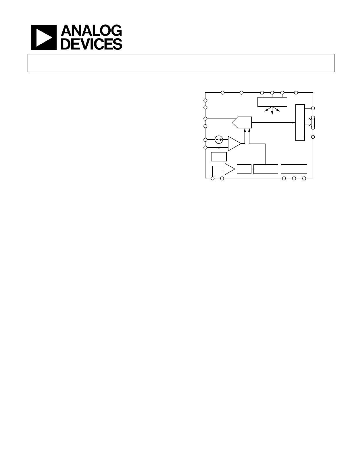
FUNCTIONAL BLOCK DIAGRAM
SPI
CSB
CONTROLS
PDWN DFSCLK+ CLK–
MODE
CMOS
OUTPUT BUFFE R
MODE
OR
D15_D14
8
D1_D0
DCO
SDIO
PROGRAMMING DATA
DUTY CYCL E
STABILIZER
Figure 1.
RBIAS
VCM
VIN+
VIN–
VREF
SENSE
GND DRVDD
DD SCLK
AD9266
ADC
CORE
REF
SELECT
DIVIDE
1TO 8
PRODUCT HIGHLIGHTS
1. The AD9266 operates from a single 1.8 V analog power
supply and features a separate digital output driver supply
to accommodate 1.8 V to 3.3 V logic families.
2. The patented sample-and-hold circuit maintains excellent
performance for input frequencies up to 200 MHz and is
designed for low cost, low power, and ease of use.
3. A standard serial port interface supports various product
features and functions, such as data output formatting,
internal clock divider, power-down, DCO and data output
(D15_D14 to D1_D0) timing and offset adjustments, and
voltage reference modes.
4. The AD9266 is packaged in a 32-lead RoHS-compliant
LFCSP that is pin compatible with the AD9609 10-bit
ADC, the AD9629 12-bit ADC, and the AD9649 14-bit
ADC, enabling a simple migration path between 10-bit and
16-bit converters sampling from 20 MSPS to 80 MSPS.
08678-001
Rev. 0
Information furnished by Analog Devices is believed to be accurate and reliable. However, no
responsibility is assumed by Analog Devices for its use, nor for any infringements of patents or other
rights of third parties that may result from its use. Specifications subject to change without notice. No
license is granted by implication or otherwise under any patent or patent rights of Analog Devices.
Trademarks and registered trademarks are the property of their respective owners.
One Technology Way, P.O. Box 9106, Norwood, MA 02062-9106, U.S.A.
Tel: 781.329.4700 www.analog.com
Fax: 781.461.3113 ©2010 Analog Devices, Inc. All rights reserved.

AD9266
TABLE OF CONTENTS
Features .............................................................................................. 1
Applications ....................................................................................... 1
Functional Block Diagram .............................................................. 1
Product Highlights ........................................................................... 1
Revision History ............................................................................... 2
General Description ......................................................................... 3
Specifications ..................................................................................... 4
DC Specifications ......................................................................... 4
AC Specifications .......................................................................... 5
Digital Specifications ................................................................... 6
Switching Specifications .............................................................. 7
Timing Specifications .................................................................. 8
Absolute Maximum Ratings ............................................................ 9
Thermal Characteristics .............................................................. 9
ESD Caution .................................................................................. 9
Pin Configuration and Function Descriptions ........................... 10
Typical Performance Characteristics ........................................... 11
AD9266-80 .................................................................................. 11
AD9266-65 .................................................................................. 13
AD9266-40 .................................................................................. 14
AD9266-20 .................................................................................. 15
Equivalent Circuits ......................................................................... 16
Theory of Operation ...................................................................... 17
Analog Input Considerations .................................................... 17
Voltage Reference ....................................................................... 19
Clock Input Considerations ...................................................... 20
Power Dissipation and Standby Mode .................................... 22
Digital Outputs ........................................................................... 22
Timing ......................................................................................... 23
Built-In Self-Test (BIST) and Output Test .................................. 24
Built-In Self-Test (BIST) ............................................................ 24
Output Test Modes ..................................................................... 24
Serial Port Interface (SPI) .............................................................. 25
Configuration Using the SPI ..................................................... 25
Hardware Interface ..................................................................... 26
Configuration Without the SPI ................................................ 26
SPI Accessible Features .............................................................. 26
Memory Map .................................................................................. 27
Reading the Memory Map Register Table ............................... 27
Open Locations .......................................................................... 27
Default Values ............................................................................. 27
Memory Map Register Table ..................................................... 28
Memory Map Register Descriptions ........................................ 30
Applications Information .............................................................. 31
Design Guidelines ...................................................................... 31
Outline Dimensions ....................................................................... 32
Ordering Guide .......................................................................... 32
REVISION HISTORY
04/10—Revision 0: Initial Version
Rev. 0 | Page 2 of 32

AD9266
GENERAL DESCRIPTION
The AD9266 is a monolithic, single-channel 1.8 V supply,
16-bit, 20 MSPS/40 MSPS/65 MSPS/80 MSPS analog-to-digital
converter (ADC). It features a high performance sample-andhold circuit and on-chip voltage reference.
The product uses multistage differential pipeline architecture
with output error correction logic to provide 16-bit accuracy at
80 MSPS data rates and to guarantee no missing codes over the
full operating temperature range.
The ADC contains several features designed to maximize
flexibility and minimize system cost, such as programmable
clock and data alignment and programmable digital test pattern
generation. The available digital test patterns include built-in
deterministic and pseudorandom patterns, along with custom
user-defined test patterns entered via the serial port interface (SPI).
A differential clock input with a selectable internal 1-to-8 divide
ratio controls all internal conversion cycles. An optional duty cycle
stabilizer (DCS) compensates for wide variations in the clock duty
cycle while maintaining excellent overall ADC performance.
The interleaved digital output data is presented in offset binary,
gray code, or twos complement format. A data output clock
(DCO) is provided to ensure proper latch timing with receiving
logic. Both 1.8 V and 3.3 V CMOS levels are supported.
The AD9266 is available in a 32-lead RoHS-compliant LFCSP
and is specified over the industrial temperature range (−40°C
to +85°C).
Rev. 0 | Page 3 of 32
AD9266
SPECIFICATIONS
DC SPECIFICATIONS
AVDD = 1.8 V; DRVDD = 1.8 V, maximum sample rate, 2 V p-p differential input, 1.0 V internal reference; AIN = −1.0 dBFS, 50% duty
cycle clock, DCS disabled, unless otherwise noted.
Table 1.
AD9266-20/AD9266-40 AD9266-65 AD9266-80
Parameter Temp
RESOLUTION Full 10 10 10 Bits
ACCURACY
No Missing Codes Full Guaranteed Guaranteed Guaranteed
Offset Error Full +0.05 ±0.30 +0.05 ±0.30 +0.05 ±0.30 % FSR
Gain Error
Differential Nonlinearity
1
Full −2.5/−2.0 −1.0 +1.0 % FSR
(DNL)
2
Full −0.9/+1.2 −0.9/+1.7 −0.9/+1.7 LSB
25°C −0.5/+0.6 −0.5/+1.0 −0.6/+1.1 LSB
Integral Nonlinearity
2
(INL)
Full ±5.5 ±6.5 ±6.2 LSB
25°C ±1.8 ±2.4 ±3.5 LSB
TEMPERATURE DRIFT
Offset Error Full ±2 ±2 ±2 ppm/°C
INTERNAL VOLTAGE
REFERENCE
Output Voltage (1 V Mode) Full 0.983 0.995 1.007 0.983 0.995 1.007 0.983 0.995 1.007 V
Load Regulation Error
Full 2 2 2 mV
at 1.0 mA
INPUT-REFERRED NOISE
VREF = 1.0 V 25°C 2.8 2.8 2.8 LSB rms
ANALOG INPUT
Input Span, VREF = 1.0 V Full 2 2 2 V p-p
Input Capacitance
Input Common-Mode
3
Full 6.5 6.5 6.5 pF
Full 0.9 0.9 0.9 V
Voltage
Input Common-Mode
Full 0.5 1.3 0.5 1.3 0.5 1.3 V
Range
REFERENCE INPUT
Full 7.5 7.5 7.5 kΩ
RESISTANCE
POWER SUPPLIES
Supply Voltage
AVDD Full 1.7 1.8 1.9 1.7 1.8 1.9 1.7 1.8 1.9 V
DRVDD Full 1.7 3.6 1.7 3.6 1.7 3.6 V
Supply Current
2
IAVDD
IDRVDD2 (1.8 V)
IDRVDD2 (3.3 V)
Full 31.4/40.7 33.2/42.5 54.5 57.6 62.5 65.7 mA
Full 1.7/3.3 5.2 6.3 mA
Full 3.0/5.9 9.3 11.6 mA
POWER CONSUMPTION
DC Input Full 57/73 98 113 mW
Sine Wave Input2
Full 60/79 63/82 107 113 124 130 mW
(DRVDD = 1.8 V)
Sine Wave Input2
Full 66/93 129 151 mW
(DRVDD = 3.3 V)
Standby Power
4
Full 40 44 44 mW
Power-Down Power Full 0.5 0.5 0.5 mW
1
Measured with 1.0 V external reference.
2
Measured with a 10 MHz input frequency at rated sample rate, full-scale sine wave, with approximately 5 pF loading on each output bit.
3
Input capacitance refers to the effective capacitance between one differential input pin and AGND.
4
Standby power is measured with a dc input and the CLK active.
Unit Min Typ Max Min Typ Max Min Typ Max
Rev. 0 | Page 4 of 32

AD9266
AC SPECIFICATIONS
AVDD = 1.8 V; DRVDD = 1.8 V, maximum sample rate, 2 V p-p differential input, 1.0 V internal reference; AIN = −1.0 dBFS, 50% duty
cycle clock, DCS disabled, unless otherwise noted.
Table 2.
1
Parameter
Temp
SIGNAL-TO-NOISE RATIO (SNR)
fIN = 9.7 MHz 25°C 78.2 77.9 77.6 dBFS
fIN = 30.5 MHz 25°C 77.6 77.5 77.3 dBFS
Full 76.7 76.6 dBFS
fIN = 70 MHz 25°C 75.8/76.4 76.6 76.6 dBFS
Full 75.5 dBFS
fIN = 200 MHz 25°C 72.1 dBFS
SIGNAL-TO-NOISE-AND-DISTORTION (SINAD)
fIN = 9.7 MHz 25°C 78.0 77.7 77.4 dBFS
fIN = 30.5 MHz 25°C 77.5 77.3 77.1 dBFS
Full 76.2 76.2 dBFS
fIN = 70 MHz 25°C 75.7/76.3 76.5 76.6 dBFS
Full 75.5 dBFS
fIN = 200 MHz 25°C 69.4 dBFS
EFFECTIVE NUMBER OF BITS (ENOB)
fIN = 9.7 MHz 25°C 12.7 12.6 12.6 Bits
fIN = 30.5 MHz 25°C 12.6 12.5 12.5 Bits
fIN = 70 MHz 25°C 12.3/12.4 12.4 12.4 Bits
fIN = 200 MHz 25°C 11.2 Bits
WORST SECOND OR THIRD HARMONIC
fIN = 9.7 MHz 25°C −97 −96 −95 dBc
fIN = 30.5 MHz 25°C −96/−93 −94 −93 dBc
Full −80 −80 dBc
fIN = 70 MHz 25°C −97/−95 −98 −95 dBc
Full −80 dBc
fIN = 200 MHz 25°C −80 dBc
SPURIOUS-FREE DYNAMIC RANGE (SFDR)
fIN = 9.7 MHz 25°C 95 95 94 dBc
fIN = 30.5 MHz 25°C 93 92 92 dBc
Full 80 80 dBc
fIN = 70 MHz 25°C 93 95 93 dBc
Full 80 dBc
fIN = 200 MHz 25°C 80 dBc
WORST OTHER (HARMONIC OR SPUR)
fIN = 9.7 MHz 25°C −102 −101 −99 dBc
fIN = 30.5 MHz 25°C −102 −101 −98 dBc
Full −89 −89 dBc
fIN = 70 MHz 25°C −101 −100 −98 dBc
Full −89 dBc
fIN = 200 MHz 25°C −86 dBc
TWO-TONE SFDR
fIN = 30.5 MHz (−7 dBFS), 32.5 MHz (−7 dBFS) 25°C 90 90 90 dBc
ANALOG INPUT BANDWIDTH 25°C 700 700 700 MHz
1
See the AN-835 Application Note, Understanding High Speed ADC Testing and Evaluation, for a complete set of definitions.
AD9266-20/AD9266-40 AD9266-65 AD9266-80
Unit Min Typ Max Min Typ Max Min Typ Max
Rev. 0 | Page 5 of 32

AD9266
DIGITAL SPECIFICATIONS
AVDD = 1.8 V; DRVDD = 1.8 V, maximum sample rate, 2 V p-p differential input, 1.0 V internal reference; AIN = −1.0 dBFS, 50% duty
cycle clock, DCS disabled, unless otherwise noted.
Table 3.
AD9266-20/AD9266-40/AD9266-65/AD9266-80
Parameter Temp
DIFFERENTIAL CLOCK INPUTS (CLK+, CLK−)
Logic Compliance CMOS/LVDS/LVPECL
Internal Common-Mode Bias Full 0.9 V
Differential Input Voltage Full 0.2 3.6 V p-p
Input Voltage Range Full GND − 0.3 AVDD + 0.2 V
High Level Input Current Full −10 +10 μA
Low Level Input Current Full −10 +10 μA
Input Resistance Full 8 10 12 kΩ
Input Capacitance Full 4 pF
LOGIC INPUTS (SCLK/DFS, MODE, SDIO/PDWN)
1
High Level Input Voltage Full 1.2 DRVDD + 0.3 V
Low Level Input Voltage Full 0 0.8 V
High Level Input Current Full −50 −75 μA
Low Level Input Current Full −10 +10 μA
Input Resistance Full 30 kΩ
Input Capacitance Full 2 pF
LOGIC INPUTS (CSB)
2
High Level Input Voltage Full 1.2 DRVDD + 0.3 V
Low Level Input Voltage Full 0 0.8 V
High Level Input Current Full −10 +10 μA
Low Level Input Current Full 40 135 μA
Input Resistance Full 26 kΩ
Input Capacitance Full 2 pF
DIGITAL OUTPUTS
DRVDD = 3.3 V
High Level Output Voltage, IOH = 50 μA Full 3.29 V
High Level Output Voltage, IOH = 0.5 mA Full 3.25 V
Low Level Output Voltage, IOL = 1.6 mA Full 0.2 V
Low Level Output Voltage, IOL = 50 μA Full 0.05 V
DRVDD = 1.8 V
High Level Output Voltage, IOH = 50 μA Full 1.79 V
High Level Output Voltage, IOH = 0.5 mA Full 1.75 V
Low Level Output Voltage, IOL = 1.6 mA Full 0.2 V
Low Level Output Voltage, IOL = 50 μA Full 0.05 V
1
Internal 30 kΩ pull-down.
2
Internal 30 kΩ pull-up.
Unit Min Typ Max
Rev. 0 | Page 6 of 32
AD9266
SWITCHING SPECIFICATIONS
AVDD = 1.8 V; DRVDD = 1.8 V, maximum sample rate, 2 V p-p differential input, 1.0 V internal reference; AIN = −1.0 dBFS, 50% duty
cycle clock, DCS disabled, unless otherwise noted.
Table 4.
AD9266-20/AD9266-40 AD9266-65 AD9266-80
Parameter Temp
CLOCK INPUT PARAMETERS
Input Clock Rate Full 80/320 520 625 MHz
Conversion Rate
CLK Period—Divide-by-1 Mode (t
1
Full 3 20/40 3 65 3 80 MSPS
) Full
CLK
50/25
15.38 12.5 ns
CLK Pulse Width High (tCH) 25.0/12.5 7.69 6.25 ns
Aperture Delay (tA) Full 1.0 1.0 1.0 ns
Aperture Uncertainty (Jitter, tJ) Full 0.1 0.1 0.1 ps rms
DATA OUTPUT PARAMETERS
Data Propagation Delay (tPD) Full
DCO Propagation Delay (t
DCO to Data Skew (t
SKEW
) Full 3
DCO
) Full 0.1
3
3
3
0.1
3 ns
3 ns
0.1 ns
Pipeline Delay (Latency) Full 9 9 9 Cycles
Wake-Up Time
2
Full 350 350 350 μs
Standby Full 600/400 300 260 ns
OUT-OF-RANGE RECOVERY TIME Full 2 2 2 Cycles
1
Conversion rate is the clock rate after the CLK divider.
2
Wake-up time is dependent on the value of the decoupling capacitors.
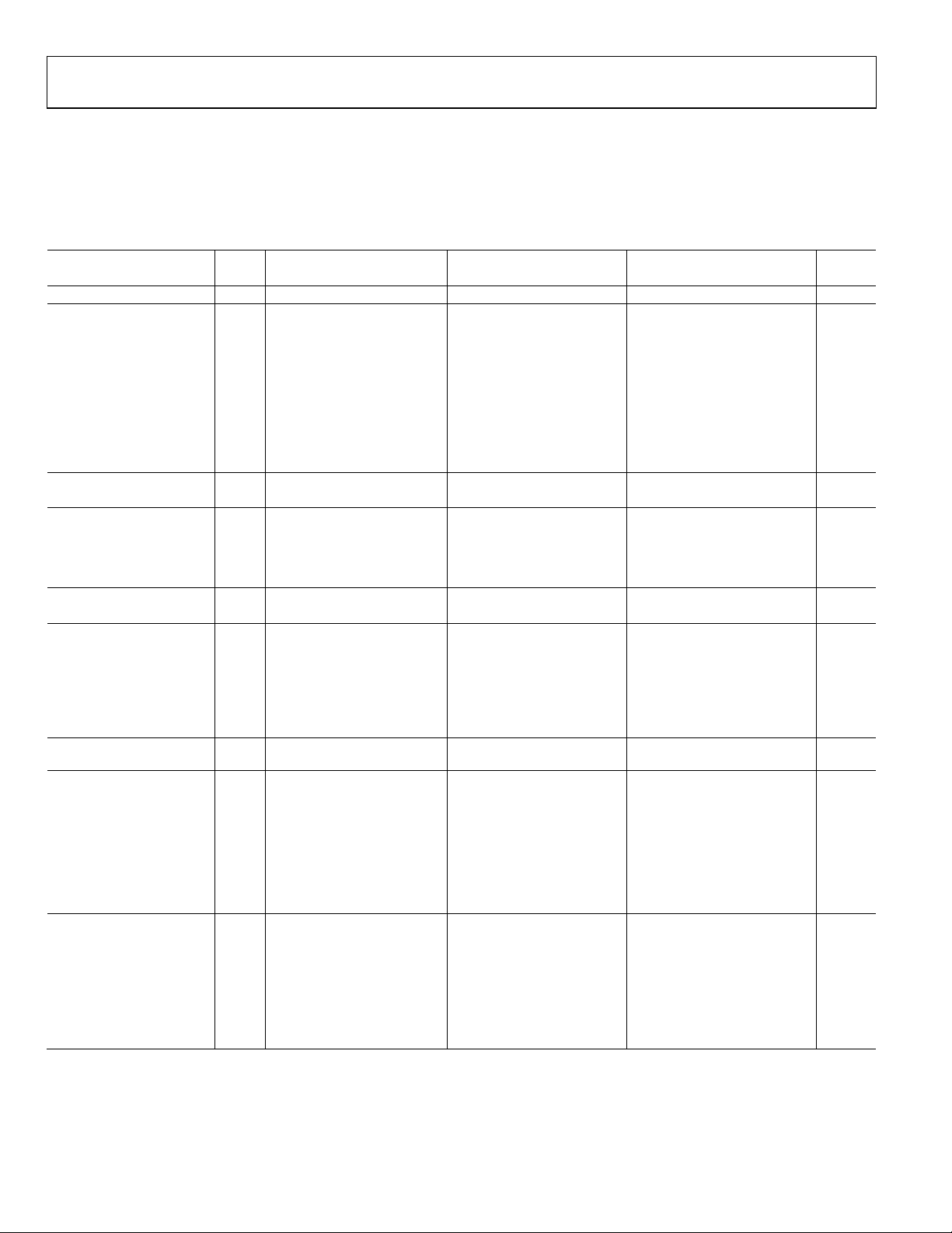
t
A
V
CLK+
CLK–
DCO
D1_D0
D15_D14
N – 1
IN
N
N + 1
D15
N + 2
t
D14
N–8
N–8
t
CLK
t
DCO
t
SKEW
D1
D0
N–9
N–9D1N–8D0N–8D1N–7D0N–7D1N–6D0N–6D1N–5D0N–5D1N–4D0N–4
t
PD
D15
D14
N–9
N–9
SKEW
D15
N + 3
D14
N–7
N–7
D15
N + 5
D14
N–6
N–6
D15
N + 6
D14
N–5
N–5
D15
N + 7
N + 8
D14
N–4
N–4
Figure 2. CMOS Output Data Timing
Unit Min Typ Max Min Typ Max Min Typ Max
8678-002
Rev. 0 | Page 7 of 32

AD9266
TIMING SPECIFICATIONS
Table 5.
Parameter Conditions Min Typ Max Unit
SPI TIMING REQUIREMENTS
tDS Setup time between the data and the rising edge of SCLK 2 ns
tDH Hold time between the data and the rising edge of SCLK 2 ns
t
Period of the SCLK 40 ns
CLK
tS Setup time between CSB and SCLK 2 ns
tH Hold time between CSB and SCLK 2 ns
t
SCLK pulse width high 10 ns
HIGH
t
SCLK pulse width low 10 ns
LOW
t
EN_SDIO
t
DIS_SDIO
Time required for the SDIO pin to switch from an input to an output
relative to the SCLK falling edge
Time required for the SDIO pin to switch from an output to an input
relative to the SCLK rising edge
10 ns
10 ns
Rev. 0 | Page 8 of 32
AD9266
ABSOLUTE MAXIMUM RATINGS
Table 6.
Parameter Rating
AVDD to AGND −0.3 V to +2.0 V
DRVDD to AGND −0.3 V to +3.9 V
VIN+, VIN− to AGND −0.3 V to AVDD + 0.2 V
CLK+, CLK− to AGND −0.3 V to AVDD + 0.2 V
VREF to AGND −0.3 V to AVDD + 0.2 V
SENSE to AGND −0.3 V to AVDD + 0.2 V
VCM to AGND −0.3 V to AVDD + 0.2 V
RBIAS to AGND −0.3 V to AVDD + 0.2 V
CSB to AGND −0.3 V to DRVDD + 0.3 V
SCLK/DFS to AGND −0.3 V to DRVDD + 0.3 V
SDIO/PDWN to AGND −0.3 V to DRVDD + 0.3 V
MODE/OR to AGND −0.3 V to DRVDD + 0.3 V
D1_D0 Through D15_D14 to AGND
DCO to AGND
−0.3 V to DRVDD + 0.3 V
−0.3 V to DRVDD + 0.3 V
Operating Temperature Range (Ambient) −40°C to +85°C
Maximum Junction Temperature Under Bias 150°C
Storage Temperature Range (Ambient) −65°C to +150°C
Stresses above those listed under Absolute Maximum Ratings
may cause permanent damage to the device. This is a stress
rating only; functional operation of the device at these or any
other conditions above those indicated in the operational
section of this specification is not implied. Exposure to absolute
maximum rating conditions for extended periods may affect
device reliability.
THERMAL CHARACTERISTICS
The exposed paddle is the only ground connection for the chip.
The exposed paddle must be soldered to the AGND plane of the
user’s circuit board. Soldering the exposed paddle to the user’s
board also increases the reliability of the solder joints and
maximizes the thermal capability of the package.
Table 7. Thermal Resistance
Package
Type
32-Lead LFCSP
5 mm × 5 mm
1
Per JEDEC 51-7, plus JEDEC 51-5 2S2P test board.
2
Per JEDEC JESD51-2 (still air) or JEDEC JESD51-6 (moving air).
3
Per MIL-Std 883, Method 1012.1.
4
Per JEDEC JESD51-8 (still air).
Airflow
Velocity
(m/sec)
1, 2
1, 3
θ
θ
JA
JC
1, 4
θ
JB
1, 2
Ψ
Unit
JT
0 37.1 3.1 20.7 0.3 °C/W
1.0 32.4 0.5 °C/W
2.5 29.1 0.8 °C/W
Typical θJA is specified for a 4-layer PCB with a solid ground
plane. As shown in Ta b l e 7 , airflow improves heat dissipation,
which reduces θ
. In addition, metal in direct contact with the
JA
package leads from metal traces, through holes, ground, and
power planes reduces the θ
.
JA
ESD CAUTION
Rev. 0 | Page 9 of 32
AD9266
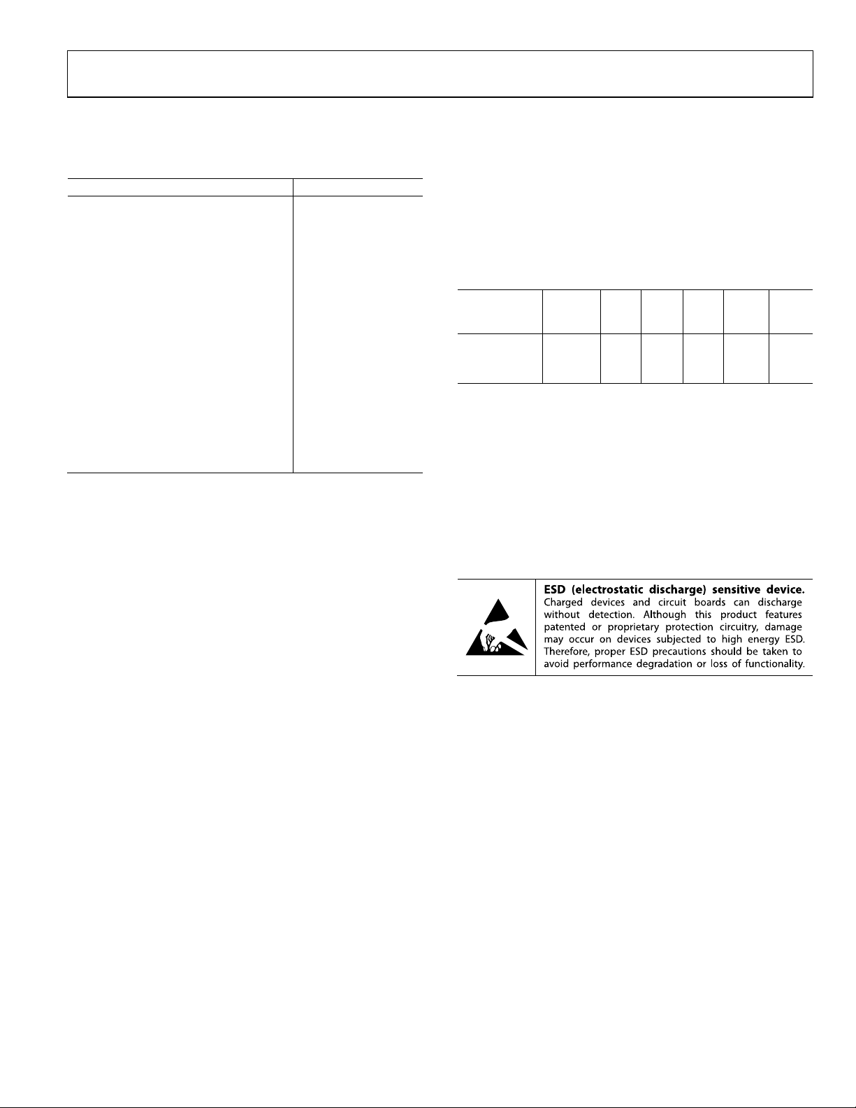
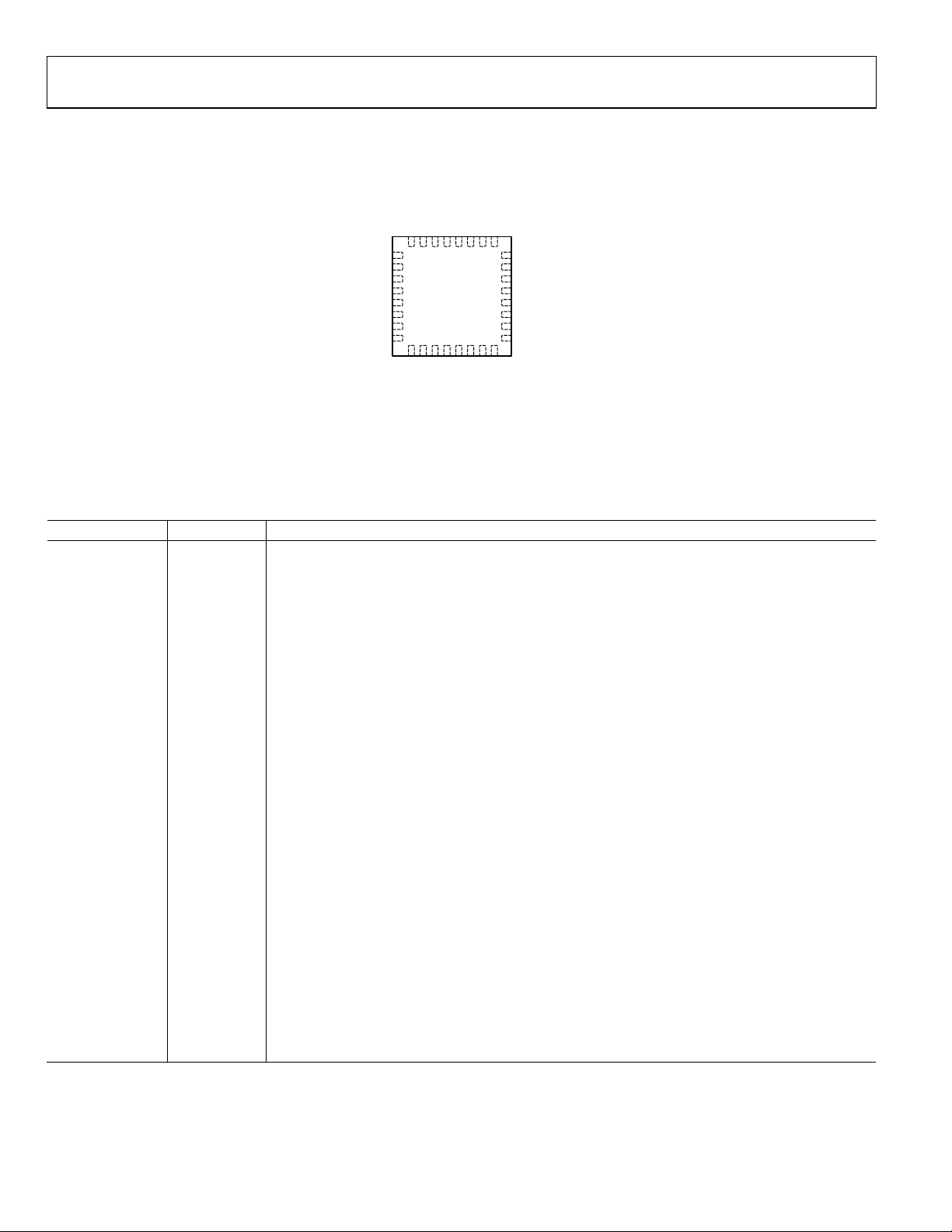
PIN CONFIGURATION AND FUNCTION DESCRIPTIONS
AVDD
VIN+
VIN–
AVDD
RBIAS
VCM
SENSE
32313029282726
CLK+
1
2
CLK–
AVDD
3
AD9266
4
CSB
SCLK/DFS
SDIO/PDWN
NC
NC
NOTES
1. NC = NO CONNE CT.
2. THE EXPOSED PADDLE (PIN 0) IS THE ONLY GND
CONNECTIO N ON THE CHIP AND MUST BE CONNECTED
TO THE PCB AGND.
5
6
7
8
TOP VIEW
(Not to S cale)
9
10111213141516
NC
NC
NC
Figure 3. Pin Configuration
Table 8. Pin Function Descriptions
Pin No. Mnemonic Description
0, Exposed Paddle AGND
The exposed paddle is the only ground connection on the chip. It must be soldered to the analog
ground of the PCB to ensure proper functionality and heat dissipation, noise, and mechanical strength
benefits.
1, 2 CLK+, CLK− Differential Encode Clock for PECL, LVDS, or 1.8 V CMOS Inputs.
3, 24, 29, 32 AVDD 1.8 V Supply Pin for ADC Core Domain.
4 CSB SPI Chip Select. Active low enable, 30 kΩ internal pull-up.
5 SCLK/DFS
SPI Clock Input in SPI Mode (SCLK). 30 kΩ internal pull-down.
Data Format Select in Non-SPI Mode (DFS). Static control of data output format. 30 kΩ internal pull-down.
DFS high = twos complement output; DFS low = offset binary output.
6 SDIO/PDWN
SPI Data Input/Output (SDIO). Bidirectional SPI data I/O with 30 kΩ internal pull-down.
Non-SPI Mode Power-Down (PDWN). Static control of chip power-down with 30 kΩ internal pull-
down. See Table 14 for details.
7 to 12 NC No Connect.
14 to 21
D1_D0 (LSB) to
(MSB) D15_D14
ADC Digital Outputs.
13 DRVDD 1.8 V to 3.3 V Supply Pin for Output Driver Domain.
22 DCO Data Clock Digital Output.
23 MODE/OR
Chip Mode Select Input (MODE)/Out-of-Range Digital Output in SPI Mode (OR).
Default = out-of-range (OR) digital output (SPI Register 0x2A, Bit 0 = 1).
Option = chip mode select input (SPI Register 0x2A, Bit 0 = 0).
Chip power-down (SPI Register 0x08, Bits[7:5] = 100b).
Chip standby (SPI Register 0x08, Bits[7:5] = 101b).
Normal operation, output disabled (SPI Register 0x08, Bits[7:5] = 110b).
Normal operation, output enabled (SPI Register 0x08, Bits[7:5] = 111b).
Out-of-range (OR) digital output only in non-SPI mode.
25 VREF 1.0 V Voltage Reference Input/Output. See Table 10.
26 SENSE Reference Mode Selection. See Table 10.
27 VCM Analog Output Voltage at Mid AVDD Supply. Sets common mode of the analog inputs.
28 RBIAS Set Analog Current Bias. Connect to 10 kΩ (1% tolerance) resistor to ground.
30, 31 VIN−, VIN+ ADC Analog Inputs.
VREF
25
AVDD
24
23
MODE/OR
DCO
22
(MSB) D15_D14
21
20
D13_D12
19
D11_D10
18
D9_D8
D7_D6
17
C
N
5_D4
(LSB)
D3_D2
D
DRVDD
D0
D1_
8678-003
Rev. 0 | Page 10 of 32
 Loading...