
High-Speed Oversampling CMOS
ADC with 16-Bit Resolution
a
FEATURES
Monolithic 16-Bit, Oversampled A/D Converter
8 Oversampling Mode, 20 MSPS Clock
2.5 MHz Output Word Rate
1.01 MHz Signal Passband w/0.004 dB Ripple
Signal-to-Noise Ratio: 88.5 dB
Total Harmonic Distortion: –96 dB
Spurious Free Dynamic Range: 100 dB
Input Referred Noise: 0.6 LSB
Selectable Oversampling Ratio: 1, 2, 4, 8
Selectable Power Dissipation: 150 mW to 585 mW
85 dB Stopband Attenuation
0.004 dB Passband Ripple
Linear Phase
Single +5 V Analog Supply, +5 V/+3 V Digital Supply
Synchronize Capability for Parallel ADC Interface
Twos-Complement Output Data
44-Lead MQFP
at a 2.5 MHz Output Word Rate
AD9260
FUNCTIONAL BLOCK DIAGRAM
VINA
VINB
REF TOP
REF
BOTTOM
COMMON
MODE
VREF
SENSE
REFCOM
AVSS
AVDD
MULTIBIT
SIGMA-DELTA
MODULATOR
AD9260
REFERENCE
BUFFER
BANDGAP
REFERENCE
AVDD
AVSS
RESET/
AVSS
AVDD
12-BIT: 20MHz
16-BIT: 10MHz
16-BIT: 5MHz
16-BIT: 2.5MHz
BIAS
CIRCUIT
SYNC
DVSS DVDD
DIGITAL
DEMODULATOR
STAGE 1:2X
DECIMATION
FILTER
STAGE 2:2X
DECIMATION
FILTER
STAGE 3:2X
DECIMATION
FILTER
CLOCK
BUFFER
MODE
REGISTER
DRVSS
DRVDD
OUTPUT REGISTER
OUTPUT MODE MULTIPLEXER
OTR
BIT1–BIT16
DAV
READ
PRODUCT DESCRIPTION
The AD9260 is a 16-bit, high-speed oversampled analog-todigital converter (ADC) that offers exceptional dynamic range
over a wide bandwidth. The AD9260 is manufactured on an
advanced CMOS process. High dynamic range is achieved with
an oversampling ratio of 8× through the use of a proprietary
technique that combines the advantages of sigma-delta and
pipeline converter technologies.
The AD9260 is a switched-capacitor ADC with a nominal fullscale input range of 4 V. It offers a differential input with 60 dB
of common-mode rejection of common-mode signals. The signal range of each differential input is ±1 V centered on a 2.0 V
common-mode level.
The on-chip decimation filter is configured for maximum performance and flexibility. A series of three half-band FIR filter
stages provide 8× decimation filtering with 85 dB of stopband
attenuation and 0.004 dB of passband ripple. An onboard digital multiplexer allows the user to access data from the various
stages of the decimation filter.
The on-chip programmable reference and reference buffer amplifier are configured for maximum accuracy and flexibility. An
external reference can also be chosen to suit the user’s specific
dc accuracy and drift requirements.
MODECLKBIAS ADJUST
CS
The AD9260 operates on a single +5 V supply, typically consuming 585 mW of power. A power scaling circuit is provided
allowing the AD9260 to operate at power consumption levels as
low as 150 mW at reduced clock and data rates. The AD9260 is
available in a 44-lead MQFP package and is specified to operate
over the industrial temperature range.
PRODUCT HIGHLIGHTS
The AD9260 is fabricated on a very cost effective CMOS
process. High-speed, precision mixed-signal analog circuits are
combined with high-density digital filter circuits.
The AD9260 offers a complete single-chip 16-bit sampling
ADC with a 2.5 MHz output data rate in a 44-lead MQFP.
Selectable Internal Decimation Filtering—The AD9260
provides a high-performance decimation filter with 0.004 dB
passband ripple and 85 dB of stopband attenuation. The filter
is configurable with options for 1×, 2×, 4×, and 8× decimation.
Power Scaling—The AD9260 consumes a low 585 mW of power
at 16-bit resolution and 2.5 MHz output data rate. Its power
can be scaled down to as low as 150 mW at reduced clock rates.
Single Supply— Both of the analog and digital portions of the
AD9260 can operate off of a single +5 V supply simplifying
system power supply design. The digital logic will also accommodate a single +3 V supply for reduced power.
REV. B
Information furnished by Analog Devices is believed to be accurate and
reliable. However, no responsibility is assumed by Analog Devices for its
use, nor for any infringements of patents or other rights of third parties
which may result from its use. No license is granted by implication or
otherwise under any patent or patent rights of Analog Devices.
One Technology Way, P.O. Box 9106, Norwood, MA 02062-9106, U.S.A.
Tel: 781/329-4700 World Wide Web Site: http://www.analog.com
Fax: 781/326-8703 © Analog Devices, Inc., 2000

AD9260–SPECIFICATIONS
CLOCK INPUT FREQUENCY RANGE
Parameter—Decimation Factor (N) AD9260 (8) AD9260 (4) AD9260 (2) AD9260 (1) Units
CLOCK INPUT (Modulator Sample Rate, f
)1111kHz min
CLOCK
20 20 20 20 MHz max
OUTPUT WORD RATE (FS = f
/N) 0.125 0.250 0.500 1 kHz min
CLOCK
2.5 5 10 20 MHz max
Specifications subject to change without notice
(AVDD = +5 V, DVDD = +3 V, DRVDD = +3 V, f
DC SPECIFICATIONS
P
arameter—Decimation Factor (N) AD9260 (8) AD9260 (4) AD9260 (2) AD9260 (1) Units
unless otherwise noted, R
BIAS
= 2 k)
= 20 MSPS, V
CLOCK
= +2.5 V, Input CML = 2.0 V T
REF
MIN
to T
RESOLUTION 16 16 16 12 Bits min
INPUT REFERRED NOISE (TYP)
1.0 V Reference 1.40 2.4 6.0 1.3 LSB rms typ
2.5 V Reference
1
0.68 (90.6) 1.2 (86) 3.7 (76) 1.0 (63.2) LSB rms typ (dB typ)
ACCURACY
Integral Nonlinearity (INL) ± 0.75 ± 0.75 ± 0.75 ± 0.3 LSB typ
Differential Nonlinearity (DNL) ±0.50 ± 0.50 ± 0.50 ± 0.25 LSB typ
No Missing Codes 16 16 16 12 Bits Guaranteed
Offset Error 0.9 (0.5) (0.5) (0.5) (0.5) % FSR max (typ @ +25°C)
Gain Error
Gain Error
2
3
2.75 (0.66) (0.66) (0.66) (0.66) % FSR max (typ @ +25°C)
1.35 (0.7) (0.7) (0.7) (0.7) % FSR max (typ @ +25°C)
TEMPERATURE DRIFT
Offset Error 2.5 2.5 2.5 2.5 ppm/°C typ
Gain Error
Gain Error
2
3
22 22 22 22 ppm/°C typ
7.0 7.0 7.0 7.0 ppm/°C typ
MAX
POWER SUPPLY REJECTION
AVDD, DVDD, DRVDD (+5 V ± 0.25 V) 0.06 0.06 0.06 0.06 % FSR max
ANALOG INPUT
Input Span
= 1.0 V 1.6 1.6 1.6 1.6 V p-p Diff. max
V
REF
= 2.5 V 4.0 4.0 4.0 4.0 V p-p Diff. max
V
REF
Input (VINA or VINB) Range +0.5 +0.5 +0.5 +0.5 V min
+AVDD – 0.5 +AVDD – 0.5 +AVDD – 0.5 +AVDD – 0.5 V max
Input Capacitance 10.2 10.2 10.2 10.2 pF typ
INTERNAL VOLTAGE REFERENCE
Output Voltage (1 V Mode) 1111 V typ
Output Voltage Error (1 V Mode) ± 14 ±14 ± 14 ±14 mV max
Output Voltage (2.5 V Mode) 2.5 2.5 2.5 2.5 V typ
Output Voltage Error (2.5 V Mode) ± 35 ± 35 ± 35 ± 35 mV max
Load Regulation
4
1 V REF 0.5 0.5 0.5 0.5 mV max
2.5 V REF 2.0 2.0 2.0 2.0 mV max
REFERENCE INPUT RESISTANCE 8888 kΩ
–2–
REV. B
P
arameter—Decimation Factor (N) AD9260 (8) AD9260 (4) AD9260 (2) AD9260 (1) Units
POWER SUPPLIES
Supply Voltages
AVDD +5 +5 +5 +5 V (± 5%)
DVDD and DRVDD +5.5 +5.5 +5.5 +5.5 V max
+2.7 +2.7 +2.7 +2.7 V min
Supply Current
IAVDD 115 115 115 115 mA typ
134 mA max
IDVDD 12.5 10.3 6.5 2.4 mA typ
3.5 mA max
IDRVDD 0.450 0.850 1.7 2.6 mA typ
POWER CONSUMPTION 613 608 600 585 mW typ
630 mW max
NOTES
1
VINA and VINB Connect to DUT CML.
2
Including Internal 2.5 V reference.
3
Excluding Internal 2.5 V reference.
4
Load regulation with 1 mA load Current (in addition to that required by AD9260).
Specifications subject to change without notice.
AC SPECIFICATIONS
(AVDD = +5 V, DVDD = +3 V, DRVDD = +3 V, f
unless otherwise noted, R
= 2 k)
BIAS
= 20 MSPS, V
CLOCK
= +2.5 V, Input CML = 2.0 V T
REF
Parameter—Decimation Factor (N) AD9260(8) AD9260(4) AD9260(2) AD9260(1) Units
DYNAMIC PERFORMANCE
INPUT TEST FREQUENCY: 100 kHz (typ)
Signal-to-Noise Ratio (SNR)
Input Amplitude = –0.5 dBFS 88.5 82 74 63 dB typ
Input Amplitude = –6.0 dBFS 82.5 78 68 58 dB typ
SNR and Distortion (SINAD)
Input Amplitude = –0.5 dBFS 87.5 82 74 63 dB typ
Input Amplitude = –6.0 dBFS 82 77.5 69 58 dB typ
Total Harmonic Distortion (THD)
Input Amplitude = –0.5 dBFS –96 –96 –97 –98 dB typ
Input Amplitude = –6.0 dBFS –93 –98 –96 –98 dB typ
Spurious Free Dynamic Range (SFDR)
Input Amplitude = –0.5 dBFS 100 98 98 88 dB typ
Input Amplitude = –6.0 dBFS 94 100 94 84 dB typ
INPUT TEST FREQUENCY: 500 kHz
Signal-to-Noise Ratio (SNR)
Input Amplitude = –0.5 dBFS 86.5 82 74 63 dB typ
80.5 dB min
Input Amplitude = –6.0 dBFS 82.5 77 68 58 dB typ
SNR and Distortion (SINAD)
Input Amplitude = –0.5 dBFS 86.0 81 74 63 dB typ
80.0 dB min
Input Amplitude = –6.0 dBFS 82.0 77 68 58 dB typ
Total Harmonic Distortion (THD)
Input Amplitude = –0.5 dBFS –97.0 –92 –89 –86 dB typ
–90.0 dB max
Input Amplitude = –6.0 dBFS –95.5 –96 –89 –86 dB typ
Spurious Free Dynamic Range (SFDR)
Input Amplitude = –0.5 dBFS 99.0 92 91 88 dB typ
90.0 dB max
Input Amplitude = –6.0 dBFS 98 100 91 82 dB typ
AD9260
to T
MIN
MAX
–3–REV. B

AD9260–SPECIFICATIONS
AC SPECIFICATIONS (Continued)
Parameter—Decimation Factor (N) AD9260 (8) AD9260 (4) AD9260 (2) AD9260 (1) Units
DYNAMIC PERFORMANCE (Continued)
INPUT TEST FREQUENCY: 1.0 MHz (typ)
Signal-to-Noise Ratio (SNR)
Input Amplitude = –0.5 dBFS 85 82 74 63 dB typ
Input Amplitude = –6.0 dBFS 80 76 68 58 dB typ
SNR and Distortion (SINAD)
Input Amplitude = –0.5 dBFS 84.5 81 74 63 dB typ
Input Amplitude = –6.0 dBFS 80 76 69 58 dB typ
Total Harmonic Distortion (THD)
Input Amplitude = –0.5 dBFS –102 –96 –82 –79 dB typ
Input Amplitude = –6.0 dBFS –96 –94 –84 –77 dB typ
Spurious Free Dynamic Range (SFDR)
Input Amplitude = –0.5 dBFS 105 98 83 80 dB typ
Input Amplitude = –6.0 dBFS 98 96 87 80 dB typ
INPUT TEST FREQUENCY: 2.0 MHz (typ)
Signal-to-Noise Ratio (SNR)
Input Amplitude = –0.5 dBFS 82 74 63 dB typ
Input Amplitude = –6.0 dBFS 76 68 58 dB typ
SNR and Distortion (SINAD)
Input Amplitude = –0.5 dBFS 81 73 62 dB typ
Input Amplitude = –6.0 dBFS 76 69 58 dB typ
Total Harmonic Distortion (THD)
Input Amplitude = –0.5 dBFS –101 –80 –75 dB typ
Input Amplitude = –6.0 dBFS –95 –80 –76 dB typ
Spurious Free Dynamic Range (SFDR)
Input Amplitude = –0.5 dBFS 104 80 78 dB typ
Input Amplitude = –6.0 dBFS 100 83 79 dB typ
INPUT TEST FREQUENCY: 5.0 MHz (typ)
Signal-to-Noise Ratio (SNR)
Input Amplitude = –0.5 dBFS 59 dB typ
Input Amplitude = –6.0 dBFS 57 dB typ
SNR and Distortion (SINAD)
Input Amplitude = –0.5 dBFS 58 dB typ
Input Amplitude = –6.0 dBFS 57 dB typ
Total Harmonic Distortion (THD)
Input Amplitude = –0.5 dBFS –58 dB typ
Input Amplitude = –6.0 dBFS –67 dB typ
Spurious Free Dynamic Range (SFDR)
Input Amplitude = –0.5 dBFS 59 dB typ
Input Amplitude = –6.0 dBFS 70 dB typ
INTERMODULATION DISTORTION
1 = 475 kHz, fIN2 = 525 kHz –93 –91 –91 –83 dBFS typ
f
IN
fIN1 = 950 kHz, fIN2 = 1.050 MHz –95 –86 –85 –83 dBFS typ
DYNAMIC CHARACTERISTICS
Full Power Bandwidth 75 75 75 75 MHz typ
Small Signal Bandwidth (AIN = –20 dBFS) 75 75 75 75 MHz typ
Aperture Jitter 2222ps rms typ
Specifications subject to change without notice.
–4–
REV. B

AD9260
DIGITAL FILTER CHARACTERISTICS
Parameter AD9260 Units
8× DECIMATION (N = 8)
Passband Ripple 0.00125 dB max
Stopband Attenuation 82.5 dB min
Passband 0 MHz min
0.605 × (f
Stopband 1.870 × (f
18.130 × (f
Passband/Transition Band Frequency
(–0.1 dB Point) 0.807 × (f
(–3.0 dB Point) 1.136 × (f
Absolute Group Delay
Group Delay Variation 0 µs max
Settling Time (to ±0.0007%)
1
1
13.55 × (20 MHz/f
24.2 × (20 MHz/f
4× DECIMATION (N = 4)
Passband Ripple 0.001 dB max
Stopband Attenuation 82.5 dB min
Passband 0 MHz min
1.24 × (f
Stopband 3.75 × (f
16.25 × (f
Passband/Transition Band Frequency
(–0.1 dB Point) 1.61 × (f
(–3.0 dB Point) 2.272 × (f
Absolute Group Delay
Group Delay Variation 0 µs max
Settling Time (to ±0.0007%)
1
1
2.90 × (20 MHz/f
5.05 × (20 MHz/f
2× DECIMATION (N = 2)
Passband Ripple 0.0005 dB max
Stopband Attenuation 85.5 dB min
Passband 0 MHz min
2.491 × (f
Stopband 7.519 × (f
12.481 × (f
Passband/Transition Band Frequency
(–0.1 dB Point) 3.231 × (f
(–3.0 dB Point) 4.535 × (f
Absolute Group Delay
Group Delay Variation 0 µs max
Settling Time (to ±0.0007%)
1
1
0.80 × (20 MHz/f
1.40 × (20 MHz/f
1× DECIMATION (N = 1)
Propagation Delay: t
PROP
13 ns max
Absolute Group Delay (225 × (20 MHz/f
NOTES
1
To determine “overall” Absolute Group Delay and/or Settling Time inclusive of delay from the sigma-delta modulator, add Absolute Group Delay and/or Settling
Time pertaining to specific decimation mode to the Absolute Group Delay specified in 1 × decimation.
Specifications subject to change without notice.
/20 MHz) MHz max
CLOCK
/20 MHz) MHz min
CLOCK
/20 MHz) MHz max
CLOCK
/20 MHz) MHz max
CLOCK
/20 MHz) MHz max
CLOCK
/20 MHz) MHz max
CLOCK
/20 MHz) MHz min
CLOCK
/20 MHz) MHz max
CLOCK
/20 MHz) MHz max
CLOCK
/20 MHz) MHz max
CLOCK
/20 MHz) MHz max
CLOCK
/20 MHz) MHz min
CLOCK
/20 MHz) MHz max
CLOCK
/20 MHz) MHz max
CLOCK
/20 MHz) MHz max
CLOCK
) µs max
CLOCK
) µs max
CLOCK
) µs max
CLOCK
) µs max
CLOCK
) µs max
CLOCK
) µs max
CLOCK
)) + t
CLOCK
PROP
ns max
–5–REV. B
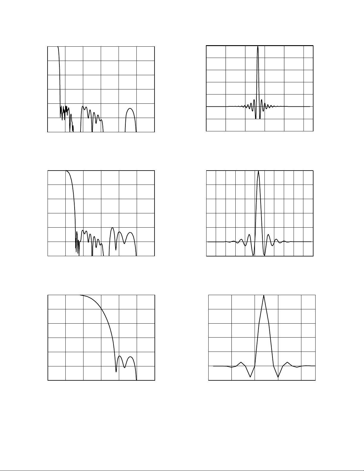
)
AD9260
–Digital Filter Characteristics
0
–20
–40
–60
MAGNITUDE – dB
–80
–100
–120
0 1.0
0.2 0.4 0.6 0.8
FREQUENCY (NORMALIZED TO
Figure 1a. 8× FIR Filter Frequency Response
0
–20
–40
–60
1.2
1.0
0.8
0.6
0.4
0.2
0
NORMALIZED OUTPUT RESPONSE
–0.2
–0.4
0 300200100
CLOCK PERIODS – RELATIVE TO CLK
400 500
Figure 1b. 8× FIR Filter Impulse Response
1.0
0.8
0.6
0.4
MAGNITUDE – dB
–80
–100
–120
0.2 0.4 0.6 0.8
0 1.0
FREQUENCY (NORMALIZED TO )
Figure 2a. 4× FIR Filter Frequency Response
0
–20
–40
–60
MAGNITUDE – dB
–80
–100
–120
0.2 0.4 0.6 0.8
0 1.0
FREQUENCY (NORMALIZED TO )
Figure 3a. 2× FIR Filter Frequency Response
1.2
1.2
0.2
0
NORMALIZED OUTPUT RESPONSE
–0.2
10 100 11020 30 40 50 60 70 80 90
0
CLOCK PERIODS – RELATIVE TO CLK
Figure 2b. 4× FIR Filter Impulse Response
1.0
0.8
0.6
0.4
0.2
0
NORMALIZED OUTPUT RESPONSE
–0.2
0
5
CLOCK PERIODS – RELATIVE TO CLK
Figure 3b. 2× FIR Filter Impulse Response
201510
–6–
REV. B

AD9260
Table I. Integer Filter Coefficients for First Stage Decimation
Filter (23-Tap Halfband FIR Filter)
Lower Upper Integer
Coefficient Coefficient Value
H(1) H(23) –1
H(2) H(22) 0
H(3) H(21) 13
H(4) H(20) 0
H(5) H(19) –66
H(6) H(18) 0
H(7) H(17) 224
H(8) H(16) 0
H(9) H(15) –642
H(10) H(14) 0
H(11) H(13) 2496
H(12) 4048
Table II. Integer Filter Coefficients for Second Stage Decimation Filter (43-Tap Halfband FIR Filter)
Lower Upper Integer
Coefficient Coefficient Value
H(1) H(43) 3
H(2) H(42) 0
H(3) H(41) –12
H(4) H(40) 0
H(5) H(39) 35
H(6) H(38) 0
H(7) H(37) –83
H(8) H(36) 0
H(9) H(35) 172
H(10) H(34) 0
H(11) H(33) –324
H(12) H(32) 0
H(13) H(31) 572
H(14) H(30) 0
H(15) H(29) –976
H(16) H(28) 0
H(17) H(27) 1680
H(18) H(26) 0
H(19) H(25) –3204
H(20) H(24) 0
H(21) H(23) 10274
H(22) 16274
NOTE: The composite filter undecimated coefficients (i.e.,
impulse response) in the 4× decimation mode can be determined
by convolving the first stage filter taps with a “zero stuffed”
version of the second stage filter taps (i.e., insert one zero between samples). Similarly, the composite filter coefficients in the
8× decimation mode can be determined by convolving the taps
of the composite 4× decimation mode (as previously determined) with a “zero stuffed” version of the third stage filter taps
(i.e., insert three zeros between samples).
Table III. Integer Filter Coefficients for Third Stage Decimation Filter (107-Tap Halfband FIR Filter)
Lower Upper Integer
Coefficient Coefficient Value
H(1) H(107) –1
H(2) H(106) 0
H(3) H(105) 2
H(4) H(104) 0
H(5) H(103) –2
H(6) H(102) 0
H(7) H(101) 3
H(8) H(100) 0
H(9) H(99) –3
H(10) H(98) 0
H(11) H(97) 1
H(12) H(96) 0
H(13) H(95) 3
H(14) H(94) 0
H(15) H(93) –12
H(16) H(92) 0
H(17) H(91) 27
H(18) H(90) 0
H(19) H(89) –50
H(20) H(88) 0
H(21) H(87) 85
H(22) H(86) 0
H(23) H(85) –135
H(24) H(84) 0
H(25) H(83) 204
H(26) H(82) 0
H(27) H(81) –297
H(28) H(80) 0
H(29) H(79) 420
H(30) H(78) 0
H(31) H(77) –579
H(32) H(76) 0
H(33) H(75) 784
H(34) H(74) 0
H(35) H(73) –1044
H(36) H(72) 0
H(37) H(71) 1376
H(38) H(70) 0
H(39) H(69) –1797
H(40) H(68) 0
H(41) H(67) 2344
H(42) H(66) 0
H(43) H(65) –3072
H(44) H(64) 0
H(45) H(63) 4089
H(46) H(62) 0
H(47) H(61) –5624
H(48) H(60) 0
H(49) H(59) 8280
H(50) H(58) 0
H(51) H(57) –14268
H(52) H(56) 0
H(53) H(55) 43520
H(54) 68508
–7–REV. B
AD9260–SPECIFICATIONS
DIGITAL SPECIFICATIONS
(AVDD = +5 V, DVDD = +5 V, T
MIN
to T
unless otherwise noted)
MAX
Parameter AD9260 Units
1
CLOCK
AND LOGIC INPUTS
High-Level Input Voltage
(DVDD = +5 V) +3.5 V min
(DVDD = +3 V) +2.1 V max
Low-Level Input Voltage
(DVDD = +5 V) +1.0 V min
(DVDD = +3 V) +0.9 V max
High-Level Input Current (V
Low-Level Input Current (V
= DVDD) ± 10 µA max
IN
= 0 V) ± 10 µA max
IN
Input Capacitance 5 pF typ
LOGIC OUTPUTS (with DRVDD = 5 V)
High-Level Output Voltage (I
High-Level Output Voltage (I
Low-Level Output Voltage
Low-Level Output Voltage (I
= 50 µA) +4.5 V min
OH
= 0.5 mA) +2.4 V min
OH
2
(IOL = 0.3 mA) +0.4 V max
= 50 µA) +0.1 V max
OL
Output Capacitance 5 pF typ
LOGIC OUTPUTS (with DRVDD = 3 V)
High-Level Output Voltage (I
= 50 µA) +2.4 V min
OH
Low-Level Output Voltage (IOL = 50 µA) +0.7 V max
NOTES
1
Since CLK is referenced to AVDD, +5 V logic input levels only apply.
2
The AD9260 is not guaranteed to meet VOL = 0.4 V max for standard TTL load of IOL = 1.6 mA.
Specifications subject to change without notice.
ANALOG INPUT
INPUT CLOCK
DATA OUTPUT
DAV
READ
CS
S1
t
CH
t
H
INPUT CLOCK
RESET
DAV
S2
t
C
t
CL
t
t
DAV
DS
t
OE
t
OD
t
DI
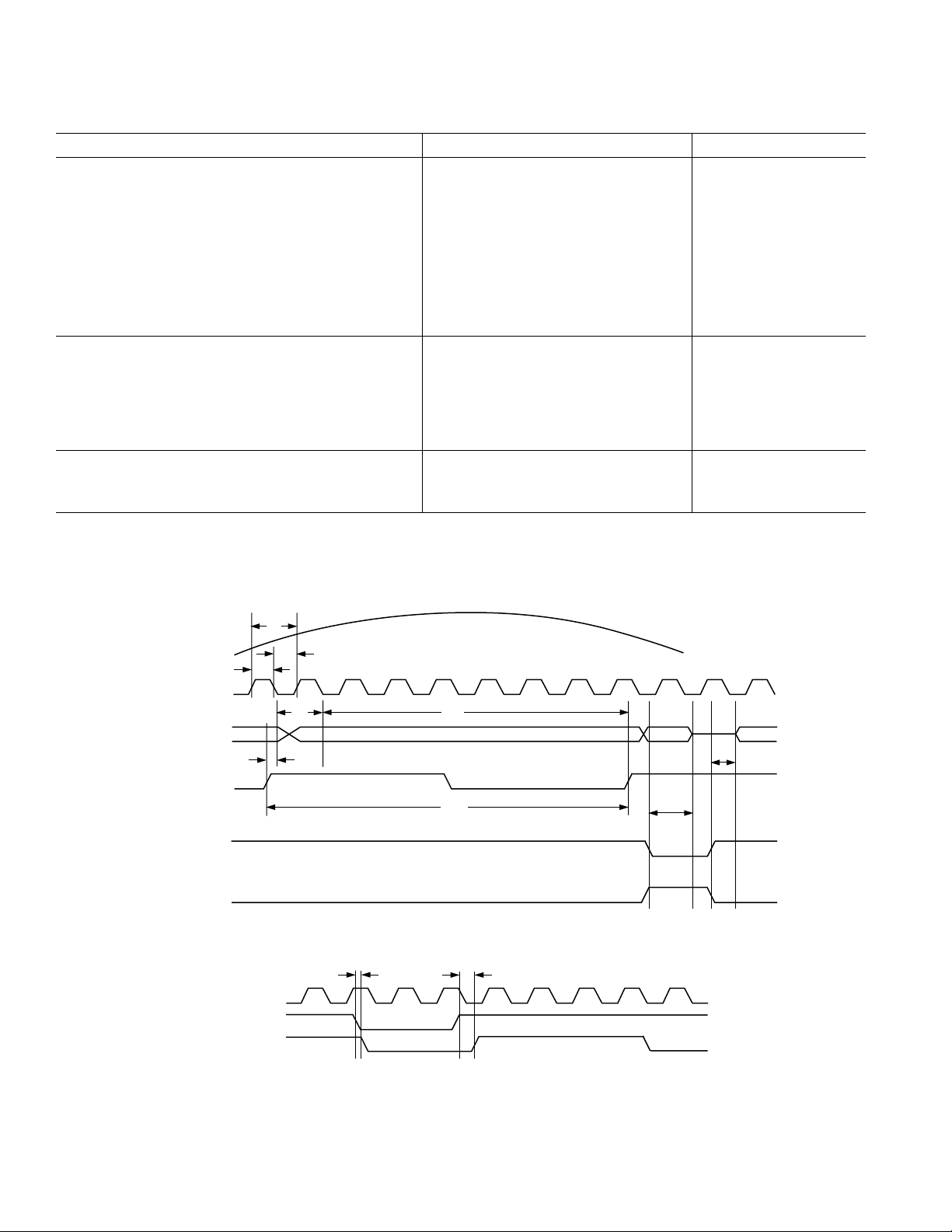
Figure 4a. Timing Diagram
t
RES-DAV
t
CLK-DAV
Figure 4b.
RESET
Timing Diagram
–8–
REV. B

AD9260
WARNING!
ESD SENSITIVE DEVICE
SWITCHING SPECIFICATIONS
(AVDD = +5 V, DVDD = +5 V, CL = 20 pF, T
MIN
to T
unless otherwise noted)
MAX
Parameters Symbol AD9260 Units
Clock Period t
Data Available (DAV) Period t
Data Invalid t
Data Setup Time t
Clock Pulsewidth High t
Clock Pulsewidth Low t
Data Hold Time t
RESET to DAV Delay t
CLOCK to DAV Delay t
Three-State Output Disable Time t
Three-State Output Enable Time t
Specifications subject to change without notice.
C
DAV
DI
DS
CH
CL
H
RES–DAV
CLK–DAV
OD
OE
ABSOLUTE MAXIMUM RATINGS*
With
Respect
Parameter to Min Max Units
AVDD AVSS –0.3 +6.5 V
DVDD DVSS –0.3 +6.5 V
AVSS DVSS –0.3 +0.3 V
AVDD DVDD –6.5 +6.5 V
DRVDD DRVSS –0.3 +6.5 V
DRVSS AVSS –0.3 +0.3 V
REFCOM AVSS –0.3 +0.3 V
CLK, MODE, READ,
Model Range Description Option*
AD9260AS –40°C to +85°C 44-Lead MQFP S-44
AD9260EB Evaluation Board
*S = Metric Quad Flatpack.
THERMAL CHARACTERISTICS
Thermal Resistance
44-Lead MQFP
θ
= 53.2°C/W
JA
= 19°C/W
θ
JC
50 ns min
tC × Mode ns min
40% t
t
–tH–t
DAV
DAV
DI
ns max
ns min
22.5 ns min
22.5 ns min
3.5 ns min
10 ns typ
15 ns typ
8 ns typ
45 ns typ
ORDERING GUIDE
Temperature Package Package
CS, RESET DVSS –0.3 DVDD + 0.3 V
Digital Outputs DRVSS –0.3 DRVDD
+ 0.3 V
VINA, VINB,
CML, BIAS AVSS –0.3 AVDD
VREF AVSS –0.3 AVDD
SENSE AVSS –0.3 AVDD
+ 0.3 V
+ 0.3 V
+ 0.3 V
CAPB, CAPT AVSS –0.3 AVDD + 0.3 V
Junction Temperature +150 °C
Storage Temperature –65 +150 °C
Lead Temperature
(10 sec) +300 °C
*Stresses above those listed under Absolute Maximum Ratings may cause perma-
nent damage to the device. This is a stress rating only; functional operation of the
device at these or any other conditions above those indicated in the operational
sections of this specification is not implied. Exposure to absolute maximum ratings
for extended periods may effect device reliability.
CAUTION
ESD (electrostatic discharge) sensitive device. Electrostatic charges as high as 4000 V readily
accumulate on the human body and test equipment and can discharge without detection.
Although the AD9260 features proprietary ESD protection circuitry, permanent damage may
occur on devices subjected to high-energy electrostatic discharges. Therefore, proper ESD
precautions are recommended to avoid performance degradation or loss of functionality.
–9–REV. B

AD9260
DEFINITIONS OF SPECIFICATION
INTEGRAL NONLINEARITY (INL)
INL refers to the deviation of each individual code from a line
drawn from “negative full scale” through “positive full scale.”
The point used as “negative full scale” occurs 1/2 LSB before
the first code transition. “Positive full scale” is defined as a
level 1 1/2 LSB beyond the last code transition. The deviation
is measured from the middle of each particular code to the true
straight line.
DIFFERENTIAL NONLINEARITY (DNL, NO MISSING
CODES)
An ideal ADC exhibits code transitions that are exactly 1 LSB
apart. DNL is the deviation from this ideal value. Guaranteed
no missing codes to 14-bit resolution indicates that all 16384
codes, respectively, must be present over all operating ranges.
NOTE: Conventional INL and DNL measurements don’t really
apply to Σ∆ converters: the DNL looks continually better if
longer data records are taken. For the AD9260, INL and DNL
numbers are given as representative.
ZERO ERROR
The major carry transition should occur for an analog value
1/2 LSB below VINA = VINB. Zero error is defined as the
deviation of the actual transition from that point.
GAIN ERROR
The first code transition should occur at an analog value
1/2 LSB above negative full scale. The last transition should
occur at an analog value 1 1/2 LSB below the nominal full scale.
Gain error is the deviation of the actual difference between first
and last code transitions and the ideal difference between first
and last code transitions.
TEMPERATURE DRIFT
The temperature drift for zero error and gain error specifies the
maximum change from the initial (+25°C) value to the value at
or T
T
MIN
POWER SUPPLY REJECTION
MAX
.
The specification shows the maximum change in full scale from
the value with the supply at the minimum limit to the value with
the supply at its maximum limit.
APERTURE JITTER
Aperture jitter is the variation in aperture delay for successive
samples and is manifested as noise on the input to the A/D.
SIGNAL-TO-NOISE AND DISTORTION (S/N+D, SINAD)
RATIO
S/N+D is the ratio of the rms value of the measured input signal
to the rms sum of all other spectral components below the
Nyquist frequency, including harmonics but excluding dc.
The value for S/N+D is expressed in decibels.
EFFECTIVE NUMBER OF BITS (ENOB)
For a sine wave, SINAD can be expressed in terms of the number of bits. Using the following formula,
N = (SINAD – 1.76)/6.02
it is possible to get a measure of performance expressed as N,
the effective number of bits.
Thus, effective number of bits for a device for sine wave inputs
at a given input frequency can be calculated directly from its
measured SINAD.
TOTAL HARMONIC DISTORTION (THD)
THD is the ratio of the rms sum of the first six harmonic components to the rms value of the measured input signal and
is expressed as a percentage or in decibels.
SIGNAL-TO-NOISE RATIO (SNR)
SNR is the ratio of the rms value of the measured input signal to
the rms sum of all other spectral components below the Nyquist
frequency, excluding the first six harmonics and dc. The value
for SNR is expressed in decibels.
SPURIOUS FREE DYNAMIC RANGE (SFDR)
SFDR is the difference in dB between the rms amplitude of the
input signal and the peak spurious signal.
TWO-TONE SFDR
The ratio of the rms value of either input tone to the rms value
of the peak spurious component. The peak spurious component
may or may not be an IMD product. May be reported in dBc
(i.e., degrades as signal level is lowered), or in dBFS (always
related back to converter full scale).
–10–
REV. B
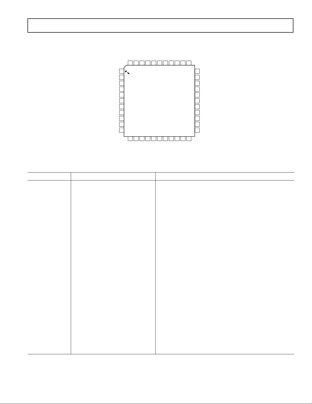
PIN CONFIGURATION
AD9260
VINB
42
BIT11
NC
VINA
CML
40 39 3841
AD9260
TOP VIEW
(Not to Scale)
BIT8
BIT9
BIT10
AVSS
BIT7
CAPT
BIT6
CAPB
BIT5
BIAS
BIT4
MODE
33
32
31
30
29
28
27
26
25
24
23
BIT3
REFCOM
VREF
SENSE
RESET
AVSS
AVDD
CS
DAV
OTR
BIT1 (MSB)
BIT2
DVSS
AVSS
DVDD
AVDD
DRVSS
DRVDD
CLK
READ
(LSB) BIT16
BIT15
BIT14
NC
AVDD
4344 36 35 3437
1
PIN 1
IDENTIFIER
2
3
4
5
6
7
8
9
10
11
12 13 14 15 16 17 18 19 20 21 2 2
BIT12
BIT13
NC = NO CONNECT
PIN FUNCTION DESCRIPTIONS
Pin No. Name Description
1 DVSS Digital Ground.
2, 29, 38 AVSS Analog Ground.
3 DVDD +3 V to +5 V Digital Supply.
4, 28, 44 AVDD +5 V Analog Supply.
5 DRVSS Digital Output Driver Ground.
6 DRVDD +3 V to +5 V Digital Output Driver Supply.
7 CLK Clock Input.
8 READ Part of DSP Interface—Pull Low to Disable Output Bits.
9 BIT16 Least Significant Data Bit (LSB).
10–23 BIT15–BIT2 Data Output Bit.
24 BIT1 Most Significant Data Bit (MSB).
25 OTR Out of Range—Set When Converter or Filter Overflows.
26 DAV Data Available.
27 CS Chip Select (CS): Active LOW.
30 RESET RESET: Active LOW.
31 SENSE Reference Amplifier SENSE: Selects REF Level.
32 VREF Input Span Select Reference I/O.
33 REFCOM Reference Common.
34 MODE Mode Select—Selects Decimation Mode.
35 BIAS Power Bias.
36 CAPB Noise Reduction Pin—Decouples Reference Level.
37 CAPT Noise Reduction Pin—Decouples Reference Level.
39 CML Common-Mode Level (AVDD/2.5).
40, 43 NC No Connect (Ground for Shielding Purposes).
41 VINA Analog Input Pin (+).
42 VINB Analog Input Pin (–).
–11–REV. B
 Loading...