

FEATURES
Single 3 V supply operation (2.7 V to 3.6 V)
SNR = 72.7 dBc to Nyquist
SFDR = 87.6 dBc to Nyquist
Low power: 366 mW
Differential input with 500 MHz bandwidth
On-chip reference and sample-and-hold
DNL = ± 0.5 LSB
Flexible analog input: 1 V p-p to 2 V p-p range
Offset binary or twos complement data format
Clock duty cycle stabilizer
APPLICATIONS
High end medical imaging equipment
IF sampling in communications receivers:
WCDMA, CDMA-One, CDMA-2000, TDS-CDMA
Battery-powered instruments
Hand-held scopemeters
Low cost digital oscilloscopes
Power sensitive military applications
GENERAL DESCRIPTION
The AD9245 is a monolithic, single 3 V supply, 14-bit, 80 MSPS
analog-to-digital converter featuring a high performance
sample-and-hold amplifier (SHA) and voltage reference. The
AD9245 uses a multistage differential pipelined architecture
with output error correction logic to provide 14-bit accuracy at
80 MSPS and guarantee no missing codes over the full operating temperature range.
The wide bandwidth, truly differential SHA allows a variety of
user-selectable input ranges and common modes, including
single-ended applications. It is suitable for multiplexed systems
that switch full-scale voltage levels in successive channels, and
for sampling single-channel inputs at frequencies well beyond
the Nyquist rate. Combined with power and cost savings over
previously available analog-to-digital converters, the AD9245 is
suitable for applications in communications, imaging, and
medical ultrasound.
A single-ended clock input is used to control all internal conversion cycles. A duty cycle stabilizer (DCS) compensates for
wide variations in the clock duty cycle while maintaining
Rev. B
Information furnished by Analog Devices is believed to be accurate and reliable.
However, no responsibility is assumed by Analog Devices for its use, nor for any
infringements of patents or other rights of third parties that may result from its use.
Specifications subject to change without notice. No license is granted by implication
or otherwise under any patent or patent rights of Analog Devices. Trademarks and
registered trademarks are the property of their respective owners.
14-Bit, 80 MSPS, 3 V A/D Converter
AD9245
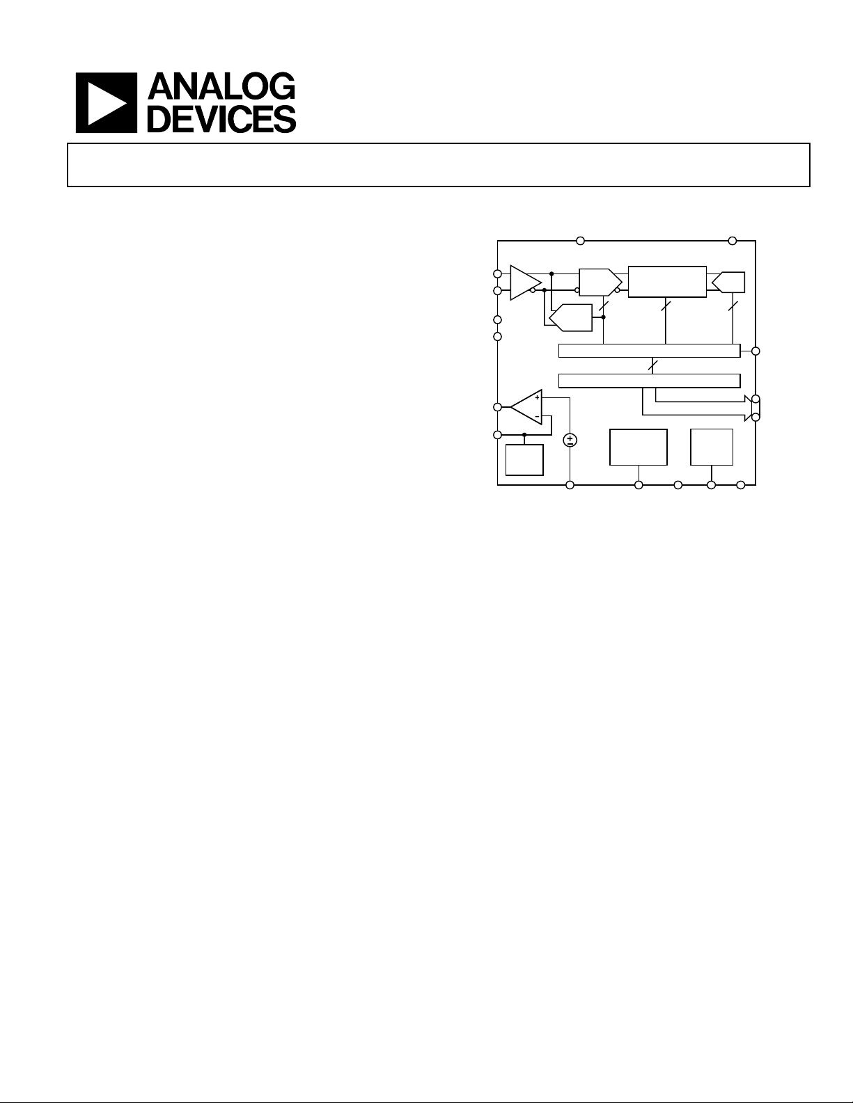
FUNCTIONAL BLOCK DIAGRAM
DRVDDAVDD
AD9245
VIN+
VIN–
REFT
REFB
VREF
SENSE
SHA
REF
SELECT
MDAC1
4 16
A/D
0.5V
AGND
Figure 1. Functional Block Diagram
excellent overall ADC performance. The digital output data is
presented in straight binary or twos complement formats. An
out-of-range (OTR) signal indicates an overflow condition that
can be used with the most significant bit to determine low or
high overflow. Fabricated on an advanced CMOS process, the
AD9245 is available in a 32-lead LFCSP and is specified over
the industrial temperature range (–40°C to +85°C).
PRODUCT HIGHLIGHTS
1. The AD9245 operates from a single 3 V power supply and
features a separate digital output driver supply to accommodate 2.5 V and 3.3 V logic families.
2. Operating at 80 MSPS, the AD9245 consumes a low 366 mW.
3. The patented SHA input maintains excellent performance for
input frequencies up to 100 MHz, and can be configured for
single-ended or differential operation.
4. The AD9245 is pin compatible with the AD9215, AD9235,
and AD9236. This allows a simplified migration from 10 bits
to 14 bits and 20 MSPS to 80 MSPS.
5. The clock DCS maintains overall ADC performance over a
wide range of clock pulsewidths.
6. The OTR output bit indicates when the signal is beyond the
selected input range.
One Technology Way, P.O. Box 9106, Norwood, MA 02062-9106, U.S.A.
Tel: 781.329.4700 www.analog.com
Fax: 781.326.8703 © 2003 Analog Devices, Inc. All rights reserved.
8-STAGE
1 1/2-BIT PIPELINE
CORRECTION LOGIC
14
OUTPUT BUFFERS
CLOCK
DUTY CYCLE
STABILIZER
CLK PDWN MODE DGND
MODE
SELECT
A/D
03583-B-001
3
OTR
D13 (MSB)
D0 (LSB)

AD9245
TABLE OF CONTENTS
AD9245–DC Specifications ............................................................ 3
Analog Input and Reference Overview ................................... 14
AD9245–AC Specifications............................................................. 4
AD9245–Digital Specifications....................................................... 5
AD9245–Switching Specifications ................................................. 6
Explanation of Test Levels........................................................... 6
Absolute Maximum Ratings............................................................ 7
Thermal Resistance ...................................................................... 7
ESD Caution.................................................................................. 7
Definitions of Specifications ........................................................... 8
Pin Configuration and Functional Descriptions.......................... 9
Equivalent Circuits......................................................................... 10
Typical Performance Characteristics ........................................... 11
Theory of Operation ...................................................................... 14
REVISION HISTORY
Revision B
Clock Input Considerations...................................................... 15
Jitter Considerations .................................................................. 16
Power Dissipation and Standby Mode .................................... 16
Digital Outputs........................................................................... 16
Timing ......................................................................................... 17
Voltage Reference....................................................................... 17
Internal Reference Connection ................................................ 17
External Reference Operation .................................................. 18
Operational Mode Selection ..................................................... 18
Evaluation Board........................................................................ 18
Outline Dimensions....................................................................... 25
Ordering Guide .......................................................................... 25
10/03—Data Sheet Changed from REV. A to REV. B
Changes to Figure 33 ..................................................................... 17
5/03—Data Sheet Changed from REV. 0 to REV. A
Changes to Figure 30 .................................................................... 15
Changes to Figure 37 ..................................................................... 19
Changes to Figure 38..................................................................... 20
Changes to Figure 39...................................................................... 21
Changes to Table 10 ....................................................................... 24
Changes to the ORDERING GUIDE........................................... 25
Rev. B | Page 2 of 28

AD9245
AD9245–DC SPECIFICATIONS
Table 1. AVDD = 3 V, DRVDD = 2.5 V, Sample Rate = 80 MSPS, 2 V p-p Differential Input, 1.0 V External Reference, unless
otherwise noted
Parameter
Temp
Test Level
Min Typ Max
RESOLUTION Full VI 14 Bits
ACCURACY
No Missing Codes Full VI Guaranteed
Offset Error1 Full VI ±0.30 ±1.2 % FSR
Gain Error 25°C V ±0.28 % FSR
Gain Error1 Full VI ±0.70 ±4.16 % FSR
Differential Nonlinearity (DNL)2 Full VI ±0.5 ±1.0 LSB
Integral Nonlinearity (INL)2 Full VI ±1.4 ±5.15 LSB
TEMPERATURE DRIFT
Offset Error1 Full V ±10 ppm/°C
Gain Error Full V ±12 ppm/°C
Gain Error1 Full V ±17 ppm/°C
INTERNAL VOLTAGE REFERENCE
Output Voltage Error (1 V Mode) Full VI ±3 ±34 mV
Load Regulation @ 1.0 mA 25°C V ±2 mV
Output Voltage Error (0.5 V Mode) 25°C V ±6 mV
Load Regulation @ 0.5 mA 25°C V ±1 mV
INPUT REFERRED NOISE
VREF = 0.5 V 25°C V 1.86 LSB rms
VREF = 1.0 V 25°C V 1.17 LSB rms
ANALOG INPUT
Input Span, VREF = 0.5 V Full IV 1 V p-p
Input Span, VREF = 1.0 V Full IV 2 V p-p
Input Capacitance3 Full V 7 pF
REFERENCE INPUT RESISTANCE Full V 7 kΩ
POWER SUPPLIES
Supply Voltage
AVDD Full IV 2.7 3.0 3.6 V
DRVDD Full IV 2.25 2.5 3.6 V
Supply Current
IAVDD2 Full VI 122 138 mA
IDRVDD2 25°C V 9 mA
PSRR 25°C V ±0.01 % FSR
POWER CONSUMPTION
Low Frequency Input4 25°C V 366 mW
Standby Power5 25°C V 1.0 mW
AD9245BCP
Unit
1
With a 1.0 V internal reference.
2
Measured at the maximum clock rate, f
3
Input capacitance refers to the effective capacitance between one differential input pin and AGND. Refer to for the equivalent analog input structure. Figure 4
4
Measured at AC Specification conditions without output drivers.
5
Standby power is measured with a dc input, CLK pin inactive (i.e., set to AVDD or AGND).
= 2.4 MHz, full-scale sine wave, with approximately 5 pF loading on each output bit.
IN
Rev. B | Page 3 of 28

AD9245
AD9245–AC SPECIFICATIONS
Table 2. AVDD = 3 V, DRVDD = 2.5 V, Sample Rate = 80 MSPS, 2 V p-p Differential Input, 1.0 V External Reference,
AIN = –0.5 dBFS, DCS Off, unless otherwise noted
Parameter
SIGNAL-TO-NOISE RATIO (SNR)
fIN = 2.4 MHz Full VI 71.1 dB
25°C V 73.3 dB
fIN = 40 MHz 25°C V 72.7 dB
fIN = 70 MHz Full IV 70.5 dB
25°C V 71.7 dB
fIN = 100 MHz 25°C V 70.2 dB
SIGNAL-TO-NOISE AND DISTORTION (SINAD)
fIN = 2.4 MHz Full VI 70.7 dB
25°C V 73.2 dB
fIN = 40 MHz 25°C V 72.5 dB
fIN = 70 MHz Full IV 69.9 dB
25°C V 71.2 dB
fIN = 100 MHz 25°C V 69.6 dB
EFFECTIVE NUMBER OF BITS (ENOB)
fIN = 2.4 MHz Full VI 11.5 Bits
25°C V 11.9 Bits
fIN = 40 MHz 25°C V 11.8 Bits
fIN = 70 MHz Full IV 11.3 Bits
25°C V 11.5 Bits
fIN = 100 MHz 25°C V 11.3 Bits
WORST SECOND OR THIRD
fIN = 2.4 MHz Full VI –76.5 dBc
25°C V –92.8 dBc
fIN = 40 MHz 25°C V –87.6 dBc
fIN = 70 MHz Full IV –75.7 dBc
25°C V –81.6 dBc
fIN = 100 MHz 25°C V –79.0 dBc
SPURIOUS-FREE DYNAMIC RANGE (SFDR)
fIN = 2.4 MHz Full VI 76.5 dBc
25°C V 92.8 dBc
fIN = 40 MHz 25°C V 87.6 dBc
fIN = 70 MHz Full IV 75.7 dBc
25°C V 81.6 dBc
fIN = 100 MHz 25°C V 79.0 dBc
Temp
Test Level
Min Typ Max
AD9245BCP
Unit
Rev. B | Page 4 of 28

AD9245
AD9245–DIGITAL SPECIFICATIONS
Table 3. AVDD = 3 V, DRVDD = 2.5 V, 1.0 V External Reference, unless otherwise noted
Parameter
LOGIC INPUTS (CLK, PDWN)
High Level Input Voltage Full IV 2.0 V
Low Level Input Voltage Full IV 0.8 V
High Level Input Current Full IV –10 +10 µA
Low Level Input Current Full IV –10 +10 µA
Input Capacitance Full V 2 pF
DIGITAL OUTPUT BITS (D0–D13, OTR)1
DRVDD = 3.3 V
High Level Output Voltage (IOH = 50 µA) Full IV 3.29 V
High Level Output Voltage (IOH = 0.5 mA) Full IV 3.25 V
Low Level Output Voltage (IOH = 1.6 mA) Full IV 0.2 V
Low Level Output Voltage (IOH = 50 µA) Full IV 0.05 V
DRVDD = 2.5 V
High Level Output Voltage (IOH = 50 µA) Full IV 2.49 V
High Level Output Voltage (IOH = 0.5 mA) Full IV 2.45 V
Low Level Output Voltage (IOH = 1.6 mA) Full IV 0.2 V
Low Level Output Voltage (IOH = 50 µA) Full IV 0.05 V
Temp
Test Level
1
Output voltage levels measured with 5 pF load on each output.
AD9245BCP
Min Typ Max
Unit
Rev. B | Page 5 of 28
AD9245
AD9245–SWITCHING SPECIFICATIONS
Table 4. AVDD = 3 V, DRVDD = 2.5 V, unless otherwise noted
AD9245BCP
Unit
Parameter
Temp
Test Level
Min Typ Max
CLOCK INPUT PARAMETERS
Maximum Conversion Rate Full VI 80 MSPS
Minimum Conversion Rate Full V 1 MSPS
CLK Period Full V 12.5 ns
CLK Pulsewidth High1 Full V 4.6 ns
CLK Pulsewidth Low1 Full V 4.6 ns
DATA OUTPUT PARAMETERS
Output Propagation Delay (tPD)2 Full V 4.2 ns
Pipeline Delay (Latency) Full V 7 Cycles
Aperture Delay (tA) Full V 1 ns
Aperture Uncertainty (Jitter, tJ) Full V 0.3 ps rms
Wake-Up Time3 Full V 7 ms
OUT-OF-RANGE RECOVERY TIME Full V 2 Cycles
1
With duty cycle stabilizer (DCS) enabled.
2
Output propagation delay is measured from CLK 50% transition to DATA 50% transition, with 5 pF load.
3
Wake-up time is dependant on the value of the decoupling capacitors; typical values shown with 0.1 µF and 10 µF capacitors on REFT and REFB.
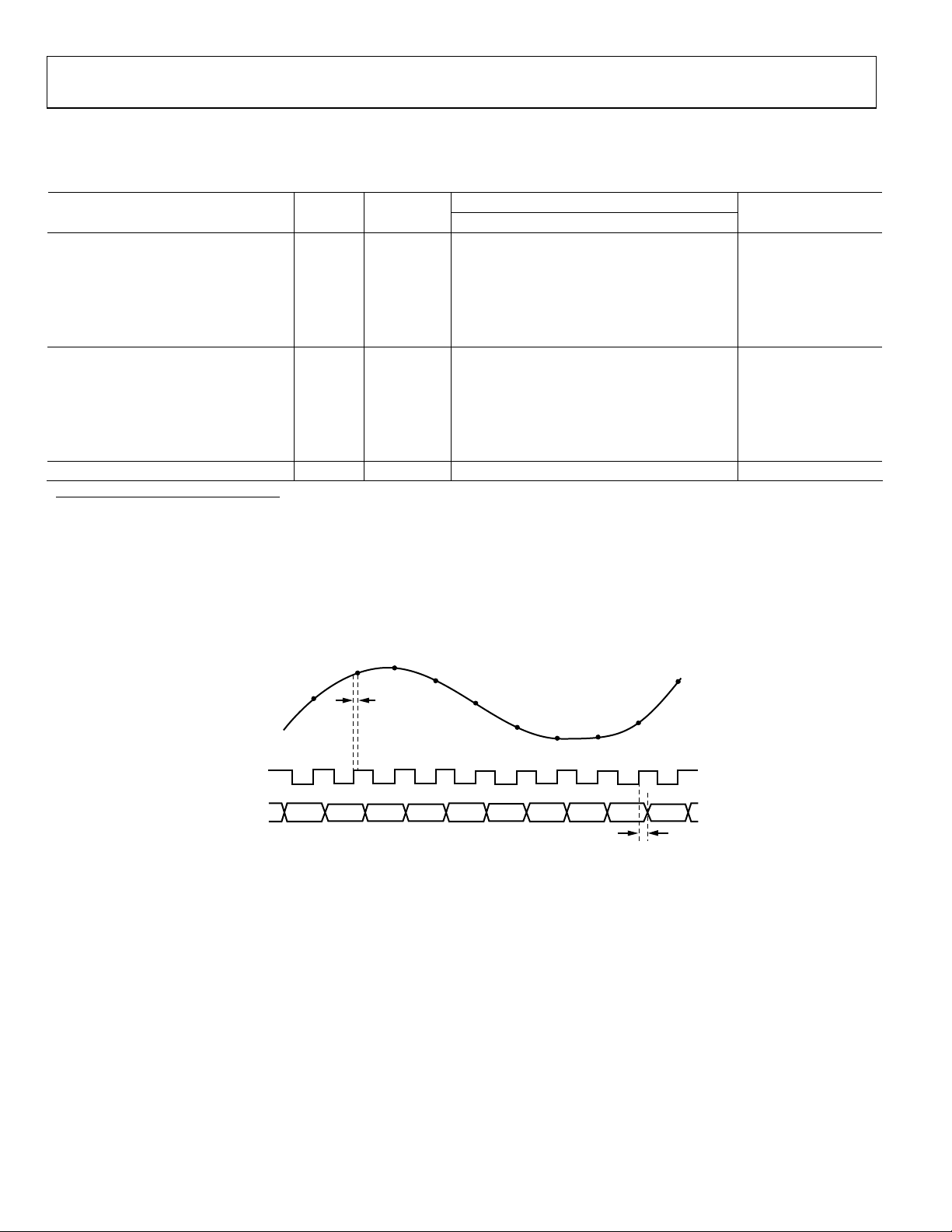
N+1
ANALOG
INPUT
CLK
DATA
OUT
N
N–1
N–9N–8N–7N–6N–5N–4N–3N–2N–1 N
t
N+2
A
Figure 2. Timing Diagram
N+3
N+4
N+5
t
= 6.0ns MAX
PD
2.0ns MIN
N+6
N+7
N+8
03583-B-002
EXPLANATION OF TEST LEVELS
Test Level Definitions
I 100% production tested.
II 100% production tested at 25°C and guaranteed by design and characterization at specified temperatures.
III Sample tested only.
IV Parameter is guaranteed by design and characterization testing.
V Parameter is a typical value only.
VI 100% production tested at 25°C and guaranteed by design and characterization for industrial temperature range.
Rev. B | Page 6 of 28
AD9245
ABSOLUTE MAXIMUM RATINGS
Table 5. AD9245 Absolute Maximum Ratings
Parameter With Respect to Min Max Unit
ELECTRICAL
AVDD AGND –0.3 +3.9 V
DRVDD DGND –0.3 +3.9 V
AGND DGND –0.3 +0.3 V
AVDD DRVDD –3.9 +3.9 V
D0–D13 DGND –0.3 DRVDD + 0.3 V
CLK, MODE AGND –0.3 AVDD + 0.3 V
VIN+, VIN– AGND –0.3 AVDD + 0.3 V
VREF AGND –0.3 AVDD + 0.3 V
SENSE AGND –0.3 AVDD + 0.3 V
REFT, REFB AGND –0.3 AVDD + 0.3 V
PDWN AGND –0.3 AVDD + 0.3 V
ENVIRONMENTAL
Storage Temperature –65 +125 °C
Operating Temperature Range –40 +85 °C
Lead Temperature Range
(Soldering 10 sec)
Junction Temperature 150 °C
300
°C
Stresses above those listed under Absolute Maximum Ratings
may cause permanent damage to the device. This is a stress
rating only and functional operation of the device at these or
any other conditions above those indicated in the operational
section of this specification is not implied. Exposure to absolute
maximum rating conditions for extended periods may affect
device reliability.
THERMAL RESISTANCE
θJA is specified for the worst-case conditions on a 4-layer board
in still air, in accordance with EIA/JESD51-1.
Table 6. Thermal Resistance
Package Type
CP-32 32.5 32.71 °C/W
θJC
θ
JA
Airflow increases heat dissipation, effectively reducing θ
Also, more metal directly in contact with the package leads
from metal traces, through holes, ground, and power planes
reduces the θ
. It is recommended that the exposed paddle be
JA
soldered to the ground plane for the LFCSP package. There is an
increased reliability of the solder joints, and maximum thermal
capability of the package is achieved with the exposed paddle
soldered to the customer board.
Unit
JA
.
ESD CAUTION
ESD (electrostatic discharge) sensitive device. Electrostatic charges as high as 4000 V readily accumulate on the
human body and test equipment and can discharge without detection. Although this product features
proprietary ESD protection circuitry, permanent damage may occur on devices subjected to high energy
electrostatic discharges. Therefore, proper ESD precautions are recommended to avoid performance
degradation or loss of functionality.
Rev. B | Page 7 of 28

AD9245
(
DEFINITIONS OF SPECIFICATIONS
Analog Bandwidth (Full Power Bandwidth)—The analog
input frequency at which the spectral power of the fundamental
frequency (as determined by the FFT analysis) is reduced by 3 dB.
Aperture Delay (t
rising edge of the clock and the instant at which the analog
input is sampled.
Aperture Uncertainty (Jitter, t
tion in aperture delay.
Integral Nonlinearity (INL)—The deviation of each individual
code from a line drawn from negative full scale through positive
full scale. The point used as negative full scale occurs ½ LSB
before the first code transition. Positive full scale is defined as a
level 1½ LSB beyond the last code transition. The deviation is
measured from the middle of each particular code to the true
straight line.
Differential Nonlinearity (DNL, No Missing Codes)—An
ideal ADC exhibits code transitions that are exactly 1 LSB apart.
DNL is the deviation from this ideal value. Guaranteed no missing codes to 14-bit resolution indicates that all 16384 codes
must be present over all operating ranges.
Offset Error—The major carry transition should occur for an
analog value ½ LSB below VIN+ = VIN–. Offset error is
defined as the deviation of the actual transition from that point.
)—The delay between the 50% point of the
A
)—The sample-to-sample varia-
J
Effective Number of Bits (ENOB)—The effective number of
bits for a sine wave input at a given input frequency can be calculated directly from its measured SINAD using the following
formula:
)
=
ENOB
Signal-to-Noise Ratio (SNR)
SINAD
1
—The ratio of the rms input
76.1−
02.6
signal amplitude to the rms value of the sum of all other spectral components below the Nyquist frequency, excluding the
first six harmonics and dc.
Spurious-Free Dynamic Range (SFDR)
1
—The difference in dB
between the rms input signal amplitude and the peak spurious
signal. The peak spurious component may or may not be a
harmonic.
1
Two -Ton e SFDR
—The ratio of the rms value of either input
tone to the rms value of the peak spurious component. The
peak spurious component may or may not be an IMD product.
Clock Pulsewidth and Duty Cycle—Pulsewidth high is the
minimum amount of time that the clock pulse should be left in
the Logic 1 state to achieve rated performance. Pulsewidth low
is the minimum time the clock pulse should be left in the
Logic 0 state. At a given clock rate, these specifications define an
acceptable clock duty cycle.
Gain Error—The first code transition should occur at an
analog value ½ LSB above negative full scale. The last transition
should occur at an analog value 1½ LSB below the positive
full scale. Gain error is the deviation of the actual difference
between first and last code transitions and the ideal difference
between first and last code transitions.
Temperature Drift—The temperature drift for offset error and
gain error specifies the maximum change from the initial
(25°C) value to the value at T
MIN
or T
MAX
.
Power Supply Rejection Ratio—The change in full scale from
the value with the supply at the minimum limit to the value
with the supply at its maximum limit.
1
Total Harmonic Distortion (THD)
—The ratio of the rms
input signal amplitude to the rms value of the sum of the first
six harmonic components.
1
Signal-to-Noise and Distortion (SINAD)
—The ratio of the
rms input signal amplitude to the rms value of the sum of all
other spectral components below the Nyquist frequency, including harmonics but excluding dc.
Minimum Conversion Rate—The clock rate at which the SNR
of the lowest analog signal frequency drops by no more than
3 dB below the guaranteed limit.
Maximum Conversion Rate—The clock rate at which parametric testing is performed.
Output Propagation Delay (t
)—The delay between the clock
PD
rising edge and the time when all bits are within valid logic
levels.
Out-of-Range Recovery Time—The time it takes for the ADC
to reacquire the analog input after a transition from 10% above
positive full scale to 10% above negative full scale, or from 10%
below negative full scale to 10% below positive full scale.
1
AC specifications may be reported in dBc (degrades as signal levels are
lowered) or in dBFS (always related back to converter full scale).
Rev. B | Page 8 of 28
AD9245
PIN CONFIGURATION AND FUNCTIONAL DESCRIPTIONS
32 AVDD
31 AGND
30 VIN–
29 VIN+
28 AGND
27 AVDD
26 REFT
25 REFB
DNC 1
CLK 2
DNC 3
PDWN 4
(LSB) D0 5
D1 6
D2 7
D3 8
(Not to Scale)
D4 9
D5 10
AD9245
CSP
TOP VIEW
D6 11
D7 12
D8 13
D9 14
Figure 3. 32-Lead LFCSP
Table 7. Pin Function Descriptions—32-Lead LFCSP (CP Package)
Pin No. Mnemonic Description
1, 3 DNC Do Not Connect
2 CLK Clock Input Pin
4 PDWN Power-Down Function Select
5 to 14, 17 to 20 D0 (LSB) to D13 (MSB) Data Output Bits
15 DGND Digital Output Ground
16 DRVDD Digital Output Driver Supply
21 OTR Out-of-Range Indicator
22 MODE Data Format Select and DCS Mode Selection (see )
23 SENSE Reference Mode Selection (see Table 8)
24 VREF Voltage Reference Input/Output
25 REFB Differential Reference (–)
26 REFT Differential Reference (+)
27, 32 AVDD Analog Power Supply
28, 31 AGND Analog Ground
29 VIN+ Analog Input Pin (+)
30 VIN– Analog Input Pin (–)
DGND 15
24 VREF
23 SENSE
22 MODE
21 OTR
20 D13 (MSB)
19 D12
18 D11
17 D10
DRVDD 16
03583-B-022
Table 9
Rev. B | Page 9 of 28

AD9245
V
EQUIVALENT CIRCUITS
AVDD
DRVDD
IN+, VIN–
03583-B
-003
Figure 4. Equivalent Analog Input Circuit
AVDD
MODE
20kΩ
03583-B
-004
Figure 5. Equivalent MODE Input Circuit
D13-D0,
OTR
03583-B
-005
Figure 6. Equivalent Digital Output Circuit
AVDD
CLK,
PDWN
03583-B
-006
Figure 7. Equivalent Digital Input Circuit
Rev. B | Page 10 of 28

AD9245
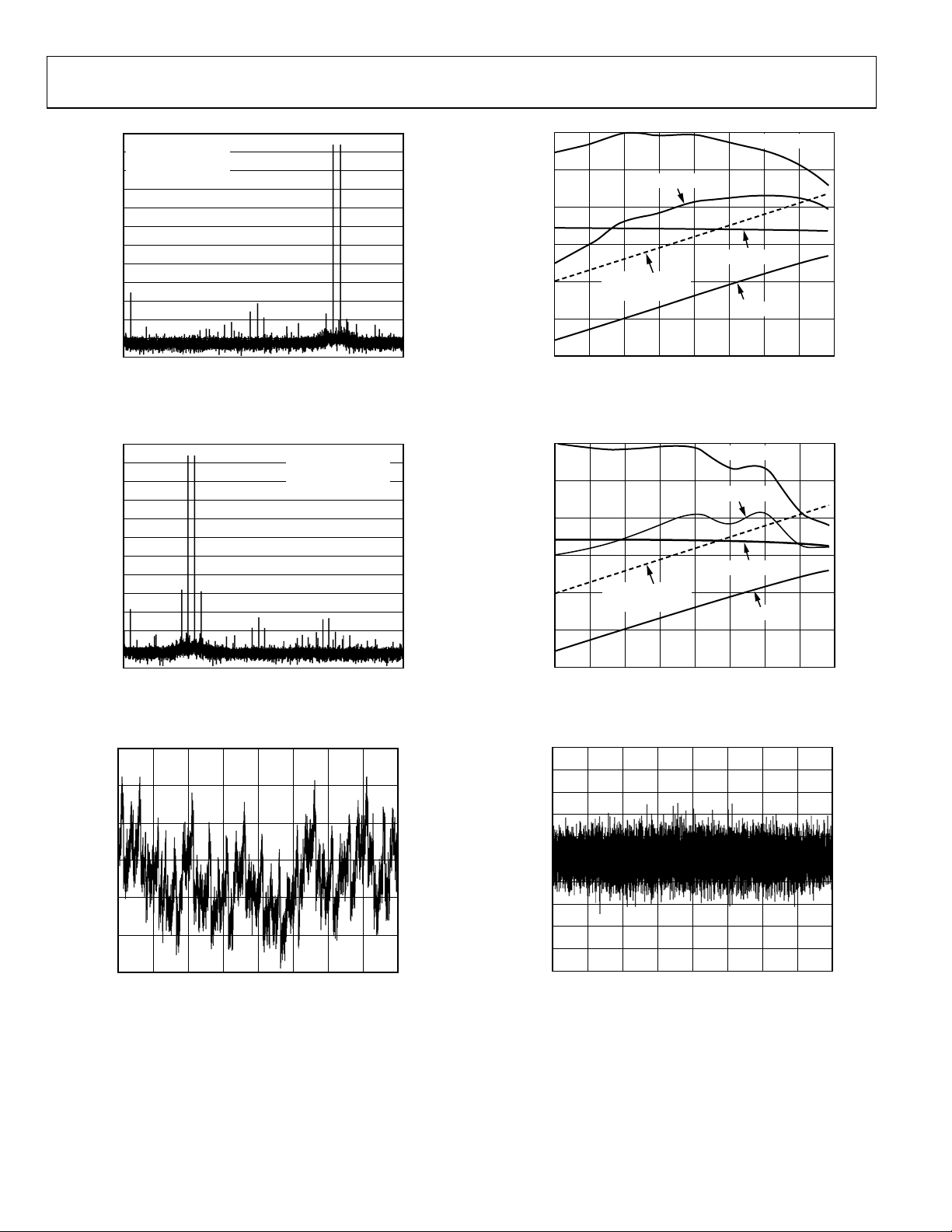
TYPICAL PERFORMANCE CHARACTERISTICS
AVDD = 3.0 V, DRVDD = 2.5 V, Sample Rate = 80 MSPS, DCS Disabled, TA = 25°C, 2 V p-p Differential Input, AIN = –0.5 dBFS,
VREF = 1.0 V External, unless otherwise noted
0
–10
–20
–30
–40
–50
–60
–70
–80
AMPLITUDE (dBFS)
–90
–100
–110
–120
0 5 10 15 20 25 30 35
FREQUENCY (MHz)
Figure 8. Single Tone 8K FFT @ 2.5 MHz
AIN = –0.5dBFS
SNR = 73.2dBc
ENOB = 11.8 BITS
SFDR = 92.8 dBc
03583-B-032
40
100
90
80
70
60
SNR/SFDR (dBc AND dBFS)
50
40
–30 –25 –20 –15 –10 –5
SFDR (dBc)
SFDR = 90dBc
REFERENCE LINE
SNR (dBc)
INPUT AMPLITUDE (dBFS)
SFDR (dBFS)
SNR (dBFS)
0
03583-B-033
Figure 11. Single Tone SNR/SFDR vs. Input Amplitude (AIN) @ 2.5 MHz
0
AIN = –0.5dBFS
SNR = 72.7dBc
–10
ENOB = 11.8 BITS
SFDR = 87.6 dBc
–20
–30
–40
–50
–60
–70
–80
AMPLITUDE (dBFS)
–90
–100
–110
–120
0 5 10 15 20 25 30 35
FREQUENCY (MHz)
Figure 9. Single Tone 8K FFT @ 39 MHz
0
–10
–20
–30
–40
–50
–60
–70
–80
AMPLITUDE (dBFS)
–90
–100
–110
–120
0 5 10 15 20 25 30 35
AIN = –0.5dBFS
SNR = 71.7dBc
ENOB = 11.5 BITS
SFDR = 81.6 dBc
FREQUENCY (MHz)
Figure 10. Single Tone 8K FFT @ 70 MHz
03583-B-023
03583-B-024
100
90
80
70
60
SNR/SFDR (dBc AND dBFS)
50
40
40
–30 –25 –20 –15 –10 –5
SFDR (dBc)
SFDR = 90dBc
REFERENCE LINE
SNR (dBc)
INPUT AMPLITUDE (dBFS)
SFDR (dBFS)
SNR (dBFS)
03583-B-034
0
Figure 12. Single Tone SNR/SFDR vs. Input Amplitude (AIN) @ 39 MHz
100
SFDR (DIFF)
90
80
70
SNR/SFDR (dBc)
60
50
40
0 20406080
SFDR (SE)
SAMPLE RATE (MSPS)
SNR (DIFF)
SNR (SE)
03583-B-025
100
Figure 13. SNR/SFDR vs. Sample Rate @ 40 MHz
Rev. B | Page 11 of 28
AD9245
0
–10
–20
–30
–40
–50
–60
–70
–80
AMPLITUDE (dBFS)
–90
–100
–110
–120
0 5 10 15 20 25 30 35
AIN = –6.5dBFS
SNR = 73.4dBFS
SFDR = 86.0dBFS
FREQUENCY (MHz)
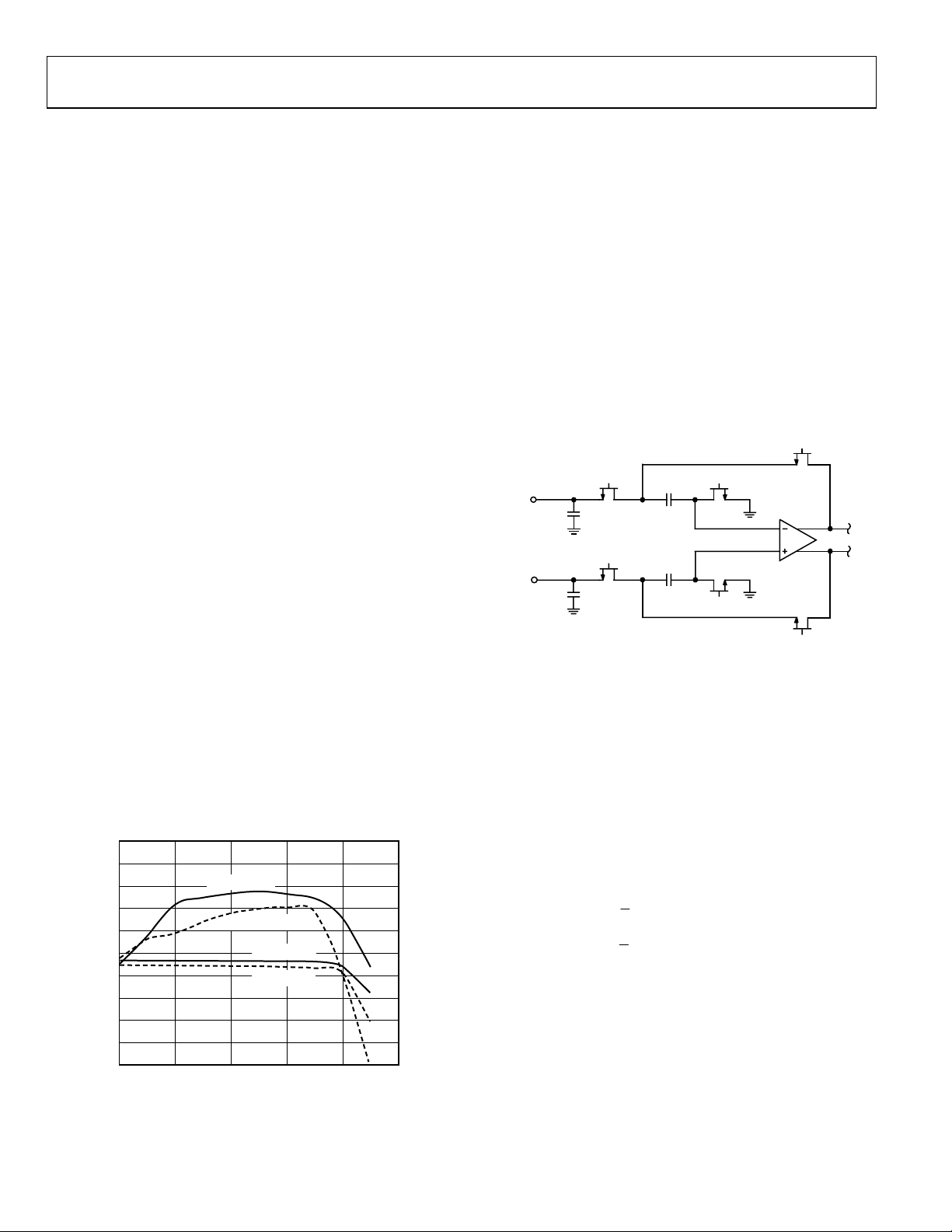
Figure 14. Two-Tone 8K FFT @ 30 MHz and 31 MHz
03583-B-029
100
90
80
70
60
SNR/SFDR (dBc AND dBFS)
50
40
40
–30 –27 –24 –21 –18 –15 –12 –9
SFDR (dBc)
SFDR = 90dBc
REFERENCE LINE
INPUT AMPLITUDE (dBFS)
SFDR (dBFS)
SNR (dBFS)
SNR (dBc)
03583-B-031
–6
Figure 17. Two-Tone SNR/SFDR vs. Input Amplitude @ 30 MHz and 31 MHz
0
–10
–20
–30
–40
–50
–60
–70
–80
AMPLITUDE (dBFS)
–90
–100
–110
–120
0 5 10 15 20 25 30 35
FREQUENCY (MHz)
AIN = –6.5dBFS
SNR = 72.7dBFS
SFDR = 78.8dBFS
Figure 15. Two-Tone 8K FFT @ 69 MHz and 70 MHz
1.5
1.0
0.5
0
INL (LSB)
–0.5
–1.0
–1.5
0 2048 4096 6144 8192 10240 12288 14336
CODE
Figure 16. Typical INL
03583-B-030
03583-B-026
40
16384
100
90
80
70
60
SNR/SFDR (dBc AND dBFS)
50
40
–30 –27 –24 –21 –18 –15 –12 –9
SFDR = 90dBc
REFERENCE LINE
INPUT AMPLITUDE (dBFS)
SFDR (dBFS)
SFDR (dBc)
SNR (dBFS)
SNR (dBc)
03583-B-027
–6
Figure 18. Two-Tone SNR/SFDR vs. Input Amplitude @ 69 MHz and 70 MHz
1.0
0.8
0.6
0.4
0.2
0
–0.2
DNL (LSB)
–0.4
–0.6
–0.8
–1.0
0 2048 4096 6144 8192 10240 12288 14336
CODE
16384
03583-B-028
Figure 19. Typical DNL
Rev. B | Page 12 of 28

AD9245
75
74
73
72
71
70
69
SNR (dBc)
68
67
66
65
0 255075100
INPUT FREQUENCY (MHz)
+85
–40
°
C
+25°C
°
C
Figure 20. SNR vs. Input Frequenc y
03583-B-036
125
100
95
90
85
SFDR (dBc)
80
+85
°
75
70
0 255075100
INPUT FREQUENCY (MHz)
C
Figure 23. SFDR vs. Input Frequen cy
–40
°
C
°
C
+25
03583-B-038
125
90
SFDR (DCS ON)
88
86
84
82
80
78
SNR/SFDR (dBc)
76
74
72
70
30 35 40 45 50 55 60 65
SFDR (DCS OFF)
DUTY CYCLE (%)
Figure 21. SNR/SFDR vs. Clock Duty Cycle
0
–10
–20
–30
–40
–50
–60
–70
–80
AMPLITUDE (dBFS)
–90
–100
–110
–120
0 9.6 19.2 28.8 38.4
FREQUENCY (MHz)
Figure 22. 32K FFT WCDMA Carrier @ F
SNR (DCS OFF)
SNR (DCS ON)
03583-B-037
03583-B-059
= 96 MHz; Sample Rate = 76.8 MSPS
IN
0
–10
–20
–30
–40
–50
–60
–70
–80
AMPLITUDE (dBFS)
–90
–100
–110
70
–120
0 9.6 19.2 28.8 38.4
FREQUENCY (MHz)
03583-B-060
Figure 24. Two 32K FFT CDMA-2000 Carriers @
= 46.08 MHz; Sample Rate = 61.44 MSPS
F
IN
0
–10
–20
–30
–40
–50
–60
–70
–80
AMPLITUDE (dBFS)
–90
–100
–110
–120
0 9.6 19.2 28.8 38.4
FREQUENCY (MHz)
03583-B-061
Figure 25. Two 32K FFT WCDMA Carriers @
FIN = 76.8 MHz; Sample Rate = 61.44 MSPS
Rev. B | Page 13 of 28
AD9245
THEORY OF OPERATION
The AD9245 architecture consists of a front-end sample and
hold amplifier (SHA) followed by a pipelined switched capacitor ADC. The pipelined ADC is divided into three sections,
consisting of a 4-bit first stage followed by eight 1.5-bit stages
and a final 3-bit flash. Each stage provides sufficient overlap to
correct for flash errors in the preceding stages. The quantized
outputs from each stage are combined into a final 14-bit result
in the digital correction logic. The pipelined architecture permits the first stage to operate on a new input sample, while the
remaining stages operate on preceding samples. Sampling
occurs on the rising edge of the clock.
Each stage of the pipeline, excluding the last, consists of a low
resolution flash ADC connected to a switched capacitor DAC
and interstage residue amplifier (MDAC). The residue amplifier
magnifies the difference between the reconstructed DAC output
and the flash input for the next stage in the pipeline. One bit of
redundancy is used in each stage to facilitate digital correction
of flash errors. The last stage simply consists of a flash ADC.
The input stage contains a differential SHA that can be accoupled or dc-coupled in differential or single-ended modes.
The output-staging block aligns the data, carries out the error
correction, and passes the data to the output buffers. The output
buffers are powered from a separate supply, allowing adjustment
of the output voltage swing. During power-down, the output
buffers go into a high impedance state.
ANALOG INPUT AND REFERENCE OVERVIEW
The analog input to the AD9245 is a differential switchedcapacitor SHA that has been designed for optimum performance while processing a differential input signal. The SHA input
can support a wide common-mode range (VCM) and maintain
excellent performance, as shown in Fi . An input
common-mode voltage of midsupply minimizes signaldependent errors and provides optimum performance.
100
95
90
85
80
75
70
SNR/SFDR (dBc)
65
60
55
50
0.5 1.0 1.5 2.0 2.5
Figure 26. SNR, SFDR vs. Common-Mode Level
SFDR (2.5MHz)
SFDR (39MHz)
COMMON-MODE LEVEL (V)
gure 26
SNR (2.5MHz)
SNR (39MHz)
03583-B-039
3.0
Referring to F , the clock signal alternately switches the
igure 27
SHA between sample mode and hold mode. When the SHA is
switched into sample mode, the signal source must be capable
of charging the sample capacitors and settling within one-half
of a clock cycle. A small resistor in series with each input can
help reduce the peak transient current required from the output
stage of the driving source. Also, a small shunt capacitor can be
placed across the inputs to provide dynamic charging currents.
This passive network creates a low-pass filter at the ADC’s
input; therefore, the precise values are dependent upon the
application. In IF undersampling applications, any shunt
capacitors should be reduced or removed. In combination with
the driving source impedance, they would limit the input
bandwidth.
H
VIN+
VIN–
T
C
PAR
T
C
PAR
Figure 27. Switched-Capacitor SHA Input
5pF
5pF
T
T
H
03583-B
-012
For best dynamic performance, the source impedances driving
VIN+ and VIN– should be matched such that common-mode
settling errors are symmetrical. These errors are reduced by the
common-mode rejection of the ADC.
An internal differential reference buffer creates positive and
negative reference voltages, REFT and REFB, that define the
span of the ADC core. The output common mode of the
reference buffer is set to midsupply, and the REFT and REFB
voltages and span are defined as follows:
1
()
2
1
()
2
()
VREFAVDDREFT
+=
VREFAVDDREFB
−=
22
VREFREFBREFTSpan
×=−×=
It can be seen from the equations above that the REFT and
REFB voltages are symmetrical about the midsupply voltage, and,
by definition, the input span is twice the value of the VREF voltage.
The internal voltage reference can be pin strapped to fixed
values of 0.5 V or 1.0 V, or adjusted within the same range as
discussed in the section.
Internal Reference Connection
Maximum SNR performance is achieved with the AD9245 set
Rev. B | Page 14 of 28

AD9245
to the largest input span of 2 V p-p. The relative SNR degradation
is 3 dB when changing from 2 V p-p mode to 1 V p-p mode.
The SHA may be driven from a source that keeps the signal
peaks within the allowable range for the selected reference voltage. The minimum and maximum common-mode input levels
are defined as
VREF
=
MIN
=
2
()
+
VREFAVDD
2
VCM
VCM
MAX
The minimum common-mode input level allows the AD9245 to
accommodate ground referenced inputs.
Although optimum performance is achieved with a differential
input, a single-ended source may be applied to VIN+ or VIN–.
In this configuration, one input accepts the signal, while the
opposite input should be set to midscale by connecting it to an
appropriate reference. For example, a 2 V p-p signal may be
applied to VIN+ while a 1 V reference is applied to VIN–. The
AD9245 then accepts an input signal varying between 2 V and
0 V. In the single-ended configuration, distortion performance
may degrade significantly as compared to the differential case.
However, the effect is less noticeable at lower input frequencies.
Differential Input Configurations
As previously detailed, optimum performance is achieved while
driving the AD9245 in a differential input configuration. For
baseband applications, the AD8138 differential driver provides
excellent performance and a flexible interface to the ADC. The
output common-mode voltage of the AD8138 is easily set to
AVDD/2, and the driver can be configured in a Sallen Key filter
topology to provide band limiting of the input signal.
33Ω
2V p-p
49.9Ω
0.1µF
10pF
33Ω
1kΩ
1kΩ
Figure 29. Differential Transformer-Coupled Configuration
The signal characteristics must be considered when selecting
a transformer. Most RF transformers saturate at frequencies
below a few MHz, and excessive signal power can also cause
core saturation, which leads to distortion.
Single-Ended Input Configuration
A single-ended input may provide adequate performance in
cost-sensitive applications. In this configuration, there is a
degradation in SFDR and distortion performance due to the
large input common-mode swing (see F ). However, if
igure 13
the source impedances on each input are matched, there should
be little effect on SNR performance. F details a typical
igure 30
single-ended input configuration.
Ω
2V p-p
1k
0.33µF
Ω
49.9
10µF 0.1µF
1k
Ω
+
Figure 30. Single-Ended Input Configuration
33
Ω
20pF
1k
Ω
33
Ω
1k
Ω
AVDD
VIN+
AD9245
VIN–
AGND
VIN+
AD9245
VIN–
03583-B
AVDD
AGND
-014
03583-B-015
1V p-p
0.1µF
1kΩ
1kΩ
49.9Ω
499Ω
523Ω
499Ω
AD8138
499Ω
33Ω
20pF
33Ω
AVDD
VIN+
AD9245
VIN–
AGND
03583-B
-013
Figure 28. Differential Input Configuration Using the AD8138
At input frequencies in the second Nyquist zone and above, the
performance of most amplifiers is not adequate to achieve the
true performance of the AD9245. This is especially true in IF
undersampling applications where frequencies in the 70 MHz to
100 MHz range are being sampled. For these applications,
differential transformer coupling is the recommended input
configuration. The value of the shunt capacitor is dependent on
the input frequency and source impedance and should be
reduced or removed. An example is shown in F . igure 29
Rev. B | Page 15 of 28
CLOCK INPUT CONSIDERATIONS
Typical high speed ADCs use both clock edges to generate a
variety of internal timing signals, and as a result may be sensitive
to clock duty cycle. Commonly a 5% tolerance is required on the
clock duty cycle to maintain dynamic performance characteristics. The AD9245 contains a clock duty cycle stabilizer (DCS) that
retimes the nonsampling edge, providing an internal clock signal
with a nominal 50% duty cycle. This allows a wide range of clock
input duty cycles without affecting the performance of the
AD9245. As shown in Figure 21, noise and distortion performance is nearly flat for a 30% to 70% duty cycle with the DCS on.
The duty cycle stabilizer uses a delay-locked loop (DLL) to
create the nonsampling edge. As a result, any changes to the
sampling frequency require approximately 100 clock cycles to
allow the DLL to acquire and lock to the new rate.

AD9245
[
]
JITTER CONSIDERATIONS
High speed, high resolution ADCs are sensitive to the quality of
the clock input. The degradation in SNR at a given input frequency (f
) due only to aperture jitter (tJ) can be calculated
INPUT
with the following equation:
tf2SNR ×π= log20
INPUT
J
In the equation, the rms aperture jitter represents the root-mean
square of all jitter sources, which include the clock input, analog
input signal, and ADC aperture jitter specification. IF undersampling applications are particularly sensitive to jitter (see Figure 31).
The clock input should be treated as an analog signal in cases
where aperture jitter may affect the dynamic range of the
AD9245. Power supplies for clock drivers should be separated
from the ADC output driver supplies to avoid modulating the
clock signal with digital noise. Low jitter, crystal controlled
oscillators make the best clock sources. If the clock is generated
from another type of source (by gating, dividing, or other methods), it should be retimed by the original clock at the last step.
75
70
65
60
55
SNR (dBc)
50
45
40
1
INPUT FREQUENCY (MHz)
Figure 31. SNR vs. Input Frequency and Jitter
0.2ps
MEASURED SNR
0.5ps
1.0ps
1.5ps
2.0ps
2.5ps
3.0ps
03583-B-041
100010010
POWER DISSIPATION AND STANDBY MODE
As shown in , the power dissipated by the AD9245 is
proportional to its sample rate. The digital power dissipation is
determined primarily by the strength of the digital drivers and
the load on each output bit. The maximum DRVDD current
(I
DRVDD
where N is the number of output bits, 14 in the case of the
AD9245. This maximum current occurs when every output bit
switches on every clock cycle, i.e., a full-scale square wave at the
Nyquist frequency, f
be established by the average number of output bits switching,
which will be determined by the sample rate and the characteristics of the analog input signal.
Figure 32
) can be calculated as
DRVDDDRVDD
/2. In practice, the DRVDD current will
CLK
NfCVI
×××=
CLKLOAD
03583-B-035
100
140
120
100
80
60
40
20
0
CURRENT (mA)
425
ANALOG CURRENT
400
TOTAL POWER
375
350
TOTAL POWER (mW)
325
DIGITAL CURRENT
300
10 20 30 40 50 60 70 80 90
Figure 32. Power and Current vs. Sample Rate @ 2.5 MHz
SAMPLE RATE (MSPS)
Reducing the capacitive load presented to the output drivers can
minimize digital power consumption. The data in was
Figure 32
taken with the same operating conditions as the Typical Performance Characteristics, and with a 5 pF load on each output
driver.
By asserting the PDWN pin high, the AD9245 is placed in
standby mode. In this state, the ADC typically dissipates
1 mW if the CLK and analog inputs are static. During standby,
the output drivers are placed in a high impedance state.
Reasserting the PDWN pin low returns the AD9245 to its
normal operational mode.
Low power dissipation in standby mode is achieved by shutting
down the reference, reference buffer, and biasing networks. The
decoupling capacitors on REFT and REFB are discharged when
entering standby mode and then must be recharged when
returning to normal operation. As a result, the wake-up time is
related to the time spent in standby mode, and shorter standby
cycles result in proportionally shorter wake-up times. With the
recommended 0.1 µF and 10 µF decoupling capacitors on REFT
and REFB, it takes approximately 1 second to fully discharge the
reference buffer decoupling capacitors and 7 ms to restore full
operation.
DIGITAL OUTPUTS
The AD9245 output drivers can be configured to interface with
2.5 V or 3.3 V logic families by matching DRVDD to the digital
supply of the interfaced logic. The output drivers are sized to provide sufficient output current to drive a wide variety of logic
families. However, large drive currents tend to cause current
glitches on the supplies that may affect converter performance.
Applications requiring the ADC to drive large capacitive loads or
large fanouts may require external buffers or latches.
As detailed in , the data format can be selected for either
offset binary or twos complement.
Table 9
Rev. B | Page 16 of 28
AD9245
TIMING
The AD9245 provides latched data outputs with a pipeline delay
of seven clock cycles. Data outputs are available one propagation delay (t
) after the rising edge of the clock signal. Refer to
PD
for a detailed timing diagram. Figure 2
The length of the output data lines and the loads placed on
them should be minimized to reduce transients within the
AD9245. These transients can degrade the converter’s dynamic
performance.
The lowest typical conversion rate of the AD9245 is 1 MSPS. At
clock rates below 1 MSPS, dynamic performance may degrade.
VOLTAGE REFERENCE
A stable and accurate 0.5 V voltage reference is built into the
AD9245. The input range can be adjusted by varying the reference voltage applied to the AD9245 using either the internal
reference or an externally applied reference voltage. The input
span of the ADC tracks reference voltage changes linearly. The
various reference modes are summarized and described
Table 8
in the following sections.
If the ADC is being driven differentially through a transformer,
the reference voltage can be used to bias the center tap (common-mode voltage).
INTERNAL REFERENCE CONNECTION
A comparator within the AD9245 detects the potential at the
SENSE pin and configures the reference into one of four
possible states, which are summarized in . If SENSE is
grounded, the reference amplifier switch is connected to the
internal resistor divider (see ), setting VREF to 1 V.
Figure 33
Connecting the SENSE pin to VREF switches the reference
amplifier output to the SENSE pin, completing the loop and
providing a 0.5 V reference output. If a resistor divider is
connected as shown in , the switch is again set to the
Figure 35
SENSE pin. This puts the reference amplifier in a noninverting
mode with the VREF output defined as follows:
Table 8
In all reference configurations, REFT and REFB drive the A/D
conversion core and establish its input span. The input range of
the ADC always equals twice the voltage at the reference pin for
either an internal or an external reference.
VIN+
10µF+0.1µF
VIN–
ADC
CORE
VREF
SELECT
LOGIC
SENSE
0.5V
AD9245
Figure 33. Internal Reference Configuration
03583-B-017
REFT
0.1µF
0.1µF 10µF
REFB
0.1µF
+
If the internal reference of the AD9245 is used to drive multiple
converters to improve gain matching, the loading of the reference by the other converters must be considered. Figure 34
depicts how the internal reference voltage is affected by loading.
0.05
0
–0.05
–0.10
ERROR (%)
–0.15
–0.20
1.0V ERROR (%)
0.5V ERROR (%)
R2
VREF 15.0
+×=
R1
–0.25
0 0.5 1.0 1.5 2.0 2.5 3.0
Figure 34. VREF Accuracy vs. Load
LOAD (mA)
0358
3-B
-019
Table 8. Reference Configuration Summary
Selected Mode
SENSE Voltage
Internal Switch
Position
Resulting VREF (V)
Resulting Differential
Span (V p-p)
External Reference AVDD N/A N/A 2 × External Reference
Internal Fixed Reference VREF SENSE 0.5 1.0
Programmable Reference 0.2 V to VREF SENSE
R2
15.0
+×
R1
(See Figure 35)
2 × VREF
Internal Fixed Reference AGND to 0.2 V Internal Divider 1.0 2.0
Rev. B | Page 17 of 28

AD9245
VIN+
VIN–
ADC
CORE
VREF
10µF+0.1µF
R2
SENSE
R1
Figure 35. Programmable Reference Configuration
SELECT
LOGIC
0.5V
AD9245
EXTERNAL REFERENCE OPERATION
The use of an external reference may be necessary to enhance
the gain accuracy of the ADC or improve thermal drift characteristics. When multiple ADCs track one another, a single
reference (internal or external) may be necessary to reduce gain
matching errors to an acceptable level. F shows the typical drift characteristics of the internal reference in both 1.0 V
and 0.5 V modes.
When the SENSE pin is tied to AVDD, the internal reference is
disabled, allowing the use of an external reference. An internal
reference buffer loads the external reference with an equivalent
7 kΩ load. The internal buffer still generates the positive and
negative full-scale references, REFT and REFB, for the ADC
core. The input span is always twice the value of the reference
voltage; therefore, the external reference must be limited to a
maximum of 1.0 V.
1.0
0.9
0.8
0.7
0.6
0.5
0.4
VREF ERROR (%)
0.3
0.2
0.1
0
–40
Figure 36. Typical VREF Drift
VREF = 1.0V
VREF = 0.5V
TEMPERATURE (°C)
igure 36
03583-B-018
REFT
0.1µF
0.1µF 10µF
REFB
0.1µF
03583-B-040
+
80706050403020100–10–20–30
OPERATIONAL MODE SELECTION
As discussed earlier, the AD9245 can output data in either offset
binary or twos complement format. There is also a provision for
enabling or disabling the clock duty cycle stabilizer (DCS). The
MODE pin is a multilevel input that controls the data format
and DCS state. The input threshold values and corresponding
mode selections are outlined in . Table 9
Table 9. Mode Selection
MODE Voltage
Data Format
Duty Cycle
Stabilizer
AVDD Twos Complement Disabled
2/3 AVDD Twos Complement Enabled
1/3 AVDD Offset Binary Enabled
AGND (Default) Offset Binary Disabled
EVALUATION BOARD
The AD9245 evaluation board provides all of the support
circuitry required to operate the ADC in its various modes and
configurations. Complete schematics and layout plots follow
and demonstrate the proper routing and grounding techniques
that should be applied at the system level.
It is critical that signal sources with very low phase noise (<1 ps
rms jitter) be used to realize the ultimate performance of the
converter. Proper filtering of the input signal, to remove
harmonics and lower the integrated noise at the input, is also
necessary to achieve the specified noise performance.
The AD9245 can be driven single-ended or differentially
through a transformer. Separate power pins are provided to
isolate the DUT from the support circuitry. Each input configuration can be selected by proper connection of various jumpers
(refer to the schematics).
An alternative differential analog input path using an AD8351
op amp is included in the layout, but is not populated in production. Designers interested in evaluating the op amp with the
ADC should remove C15, R12, and R3, and populate the op
amp circuit. The passive network between the AD8351 outputs
and the AD9245 allows the user to optimize the frequency
response of the op amp for the application.
Rev. B | Page 18 of 28

AD9245
X
X
X
X
X
1
2
Ω
0
2
2
2
P
R
)
B
S
M
(
P4
GND
0.1µF
C29
C11
10µF
R
D
6
1
1
5
1
2
GND
3
1
D
1
1
D
D
4131211
1
456
3
17
18
19
20
21
22
23
24
C7
0.1µF
6
6
E
E
L
L
O
O
H
H
T
T
1
H
M
H2M
D
N
G
1
P6
AVDD
EXTREF
1V MAX E1
6
6
E
E
L
L
O
O
H
H
T
T
H4M
H3M
P2
6
45
123
MODE
2
2
Ω
5
k
R
1
C22
10µF
C13
0.10µF
P11
AVDD
P8
P9
GND
R1
10kΩ
5.0V
VAMP
VDL
2.5V
GND
2.5V
DRVDD
GND
3.0V
AVD D
P5
P1
GND
GND
D
C
E
B
A
P7
3
P3
Ω
7
k
R
1
P10
0.1µF
R9
T
I
B
E
G
N
A
R
R
E
V
O
C8
0.1µF
GND
4
Ω
6
k
R
1
C9
0.10µF
C12
10kΩ
GND GND
X
X
X
0
7
8
9
1
D
D
D
D
0
9
1
8
7
D10
D11
D12
D13
OTR
MODE
SENSE
VREF
REFB
25262728293031
GND
2
4
Ω
R
0
C60
X
X
X
X
6
5
4
D
D
D
5
6
1
1413121
1
2
1
345
D
D
D
V
N
R
G
D
5
6
1
14131
1
D
9
D
N
D
D
V
G
D
D
0
211
1
8
7
6
5
D
D
D
D
U4
AD9245
D
D
T
F
D
E
V
A
R
D
D
V
A
D
N
G
6
Ω
2
k
R
1
6
Ω
3
k
R
1
D
D
V
A
N
I
P
M
A
F
µ
1
.
D
–
+
N
N
N
N
G
G
I
I
A
V
A
V
+
–
D
D
N
N
I
I
N
N
V
V
G
G
1
2
C
Ω
4
3
R
3
2
1
Ω
R
0
OUT
X
T 1
D
D
V
A
32
F
p
0
1
3
D
9
4
D
D
D
V
A
0
1
R
ADT1–1WT
1
L
X
2
D
Ω
6
3
H
n
0
1
1
J
X
1
D
1
678
D
N
G
F
6
p
2
0
C
1
5
4
E
CT
6
2
5
1
XFRIN1
X
0
D
0
9
1
)
B
S
L
(
D3
D2
D1
D0
PDWN
DNC
CLK
DNC
9
1
C
F
p
5
1
X
R2X
D
D
N
N
G
G
5
C
F
µ
6
1
1
.
C
0
C
E
S
I
R
34
P
NC
D
N
G
F
µ
5
1
1
.
C
0
P
M
A
F
N
F
O
O
S
S
C
C
D
D
/
/
Y
Y
R
R
A
A
N
N
I
I
B
B
T
T
E
E
S
S
F
F
F
F
O
O
:
:
3
4
O
O
T
T
5
5
D
N
G
5
2
R
3
1
R
D
D
V
A
F
µ
0
1
.
0
R SINGLE ENDED
R18
25Ω
R3, R17, R18
03583-B-050
Ω
k
1
Ω
k
1
D
N
G
ONLY ONE SHOULD BE
ON BOARD AT A TIME
)
T
L
U
A
:
R
E
P
M
U
J
E
L
B
A
R
E
D
L
O
S
N
I
P
E
S
N
E
S
D
N
G
Ω
6
3
D
N
G
OPTIONAL XFRT2FT C1–1–13
F
E
R
E
D
I
V
I
D
E
G
A
T
L
O
V
L
A
N
R
E
T
X
E
:
A
O
T
E
3
2
C
B
OUT
X
F
D
F
(
E
C
E
N
C
E
N
R
E
E
R
F
E
E
F
R
E
V
R
1
L
L
A
A
N
N
R
R
E
E
T
T
X
N
I
E
:
:
B
C
O
O
T
T
E
E
K
L
C
F
p
0
1
R30
5
1
N
E
O
O
C
:
N
S
S
R
E
E
C
C
R
P
D
D
/
/
E
M
T
T
F
U
N
N
E
J
E
E
R
E
M
M
V
L
E
E
5
.
B
L
L
0
A
P
P
L
R
M
M
E
A
O
O
D
N
C
C
L
R
S
S
O
E
O
O
T
S
N
W
W
I
N
I
T
T
:
P
:
:
D
1
2
E
D
O
O
O
T
O
T
T
E
M
5
5
D
N
G
Ω
8
k
R
1
P13
P14
D
D
V
A
5
Ω
1
3
R
3
8
1
C
Ω
B
N
I
P
M
A
B
T
OUT
OUT
C
X
X
C
4
2
E
S
I
R
3
P
D
N
I
N
R
G
F
X
Ω
0
2
2
1
P
R
8
7
6
5
4
3
2
1
R
E
T
L
I
1
F
L
R
R
O
O
F
F
µ
1
.
0
1
1
R
D
N
G
Figure 37. LFCSP Evaluation Board Schematic—Analog Inputs and DUT
Rev. B | Page 19 of 28

AD9245
9
3
517
1
325
7
9
1
3
3
9
111
5
7
1
3
1
0
4
R
E
D
A
E
H
4
2
4
6
2
D
N
R
G
D
Y
R
D
D
D
N
N
G
G
3
4
2
1
2
2
2
2
4
7
3
2
6
1
1
H
U
T
V
L
4
7
2OE
2CLK
5
2
C
A
D
/
T
A
K
L
C
2QB
2DB
DRX
B
S
M
2Q7
GND
2D7
GND
6
7
8
2
2
2
GND
D13X
5
6
D
N
G
B
S
M
2Q6
2D6
D12X
8
0
2
293
7
8
2Q5
2D5
D11X
1
9
1
012
1
0
1
121
D
D
V
R
D
9
8
1
1
CC
2Q4
V
CC
2D4
V
0
1
3
D10X
DRVDD
1
1
2
2
222
3
1
6
3
1
2
2
2
1Q8
1D8
D6X
4
2
1
373
325
2
4
2
6
2
111
1Q7
1D7
8
D5X
2
628
2
283
D
N
G
0
D
N
G
GND
9
3
GND
7
2
1Q6
1D6
D4X
9
3
5
7
1
1
1
1
0
4
6
8
2
1
1
1
0
4
6
8
2
1
1
D
N
G
5
7
6
4
1
1
1
1
2Q3
2Q2
2Q1
GND
2D3
2D2
2D1
GND
4
2
3
5
3
3
3
3
D7X
D8X
D9X
GND
2
9
2
0
3
0
9
1Q5
1D5
041
4
D3X
3
1
3
234
3
D
D
V
R
D
8
V
V
2
3
CC
CC
DRVDD
5
3
373
3
3
5
3
3
4
6
3
3
8
6
3
3
Y
R
D
7
5
6
4
3
Q
Q
1
1
1D4
1D3
3
4
2
4
4
4
D1X
D2X
7
3
8
3
0
4
D
N
G
4
D
N
G
GND
546
4
GND
9
9
3
0
4
1Q2
1D2
D0X
B
S
L
D
N
G
B
N
I
P
M
4
Ω
1
5
R
2
M
S
C
O
O
P
V
V
0
9
1
AD8351
1
2
N
1
D
P
W
G
P
R
8
2
C
N
I
P
M
A
A
I
H
P
O
8
3
I
H
N
I
F
µ
1
.
0
P
M
A
D
N
G
D
D
N
N
G
D
N
G
9
Ω
3
k
R
1
8
Ω
3
k
R
1
P
M
A
V
D
N
G
3
2
1
T
U
O
1Q1
1OE
1
N
I
1D1
1CLK
7
8
4
4
C
A
D
/
T
A
L
K
L
C
G
F
4
µ
2
0
C
1
P
M
A
V
F
µ
5
1
4
.
C
0
F
µ
4
1
4
.
C
0
D
N
G
1
4
N
R
W
R
O
D
O
0
R
4
E
R
W
E
O
S
P
U
U3
Ω
0
k
4
0
R
1
D
N
G
Ω
1
k
4
0
R
1
P
M
A
V
03583-B-051
N
I
P
M
A
F
F
µ
µ
7
7
2
C
6
1
R
O
L
P
O
7
4
O
L
N
I
1
1
1
.
.
C
0
0
7
1
Ω
Ω
0
R
0
D
N
G
M
M
O
C
6
Ω
k
4
2
3
.
R
1
5
2
G
P
R
3
Ω
3
5
R
2
F
µ
0
5
1
3
.
C
0
5
Ω
3
5
R
2
D
D
N
N
G
G
D
N
9
1
R
G
Ω
0
5
Figure 38. LFCSP Evaluation Board Schematic—Digital Path
Rev. B | Page 20 of 28

AD9245
C40
0.001µF
03583-B-052
C37
C46
0.1µF
10µF
C20
10µF
VDL
C48
DRVDD
C41
C47
C1
C39
C38
C36
C34
C31
C30
C2
GND
C49
0.001µF
0.001µF
0.1µF
0.1µF
0.001µF
0.001µF
0.1µF
0.1µF
0.1µF
0.001µF
22µF
GND
0.1µF
VAMP
LATCH BYPASSING
GND
Rx
DNP
R37
25Ω
CLKLAT/DAC
SCHEMATIC SHOWS TWO GATE DELAY SETUP.
FOR ONE DELAY, REMOVE R22 AND R37 AND
ATTACH Rx (Rx = 0Ω).
0Ω
R23
367
1Y
B
A
1
1
1
245
R32
A
2
2Y
1kΩ
GND
8
11
GND
B
2
ENCX
74VCX86
R22
0Ω
DR
VDL
14
PWR
4Y
3Y
A
3
9
B
3
10
GND
U5
B
A
4
4
12
13
R20
1kΩ
GND
R21
1kΩ
GND
R24
1kΩ
GND
E51
CLK
R28
ENC
E50
0Ω
ENCX
R27
0Ω
ENC
C14
0.001µF
C33
0.1µF
C32
0.001µF
C25
10µF
AVDD
C3
DRVDD AVDD
C4
VDL
10µF
C10
ANALOG BYPASSING DIGITAL BYPASSING LATCH BYPASSING
GND
10µF
GND
22µF
DUT BYPASSING
CLOCK TIMING ADJUSTMENTS
FOR A DIRECT ENCODE USE R27
FOR A BUFFERED ENCODE USE R28
E52 E53
VDL
VDL
R31
1kΩ
VDL
C43
0.1µF
ENCODE
J2
E31 E35
R30
R29
VDL
E43 E44
1kΩ
GND
50Ω
GND
GND
VDL
Figure 39. LFCSP Evaluation Board Schematic— Clock Input
Rev. B | Page 21 of 28

AD9245
Figure 40. LFCSP Evaluation Board Layout, Primary Side
03583-B-055
03583-B-053
Figure 42. LFCSP Evaluation Board Layout, Ground Plane
03583-B-054
Figure 41. LFCSP Evaluation Board Layout, Secondary Side
Rev. B | Page 22 of 28
03583-B-056
Figure 43. LFCSP Evaluation Board Layout, Power Plane

AD9245
Figure 44. LFCSP Evaluation Board Layout, Primary Silkscreen
03583-B-057
Figure 45. LFCSP Evaluation Board Layout, Secondary Silkscreen
03583-B-058
Rev. B | Page 23 of 28

AD9245
Table 10. LFCSP Evaluation Board Bill of Materials
Recommended
Item Qty. Omit1 Reference Designator Device Package Value
C1, C5, C7, C8, C9, C11, C12,
18
1
8
8
2
2 C46, C24
3 8
4 3 C19, C21, C23 Chip Capacitor 0603 10 pF
5 1 C26 Chip Capacitor 0603 10 pF
9
6
2 E1, E45
7 2 J1, J2 SMA Connector/50 Ω SMA
8 1 L1 Inductor 0603 10 nH
9 1 P2 Terminal Block TB6
10 1 P12 Header Dual 20-Pin RT Angle HEADER40 Digi-Key S2131-20-ND
5 R3, R12, R23, R28, Rx
11
6 R16, R17, R22, R27, R42, R37
12 2 R4, R15 Chip Resistor 0603 33 Ω
13 14
14 2 R10, R11 Chip Resistor 0603 36 Ω
1 R29
15
1 R19
16 2 RP1, RP2 Resistor Pack R_742 220 Ω
17 1 T1 ADT1-1WT AWT1-1T Mini-Circuits
18 1 U1 74LVTH162374 CMOS Register TSSOP-48
19 1 U4 AD9245BCP ADC (DUT) CSP-32 Analog Devices, Inc. X
20 1 U5 74VCX86M SOIC-14 Fairchild
21 1 PCB AD92XXBCP/PCB PCB Analog Devices, Inc. X
22 1 U3 AD8351 Op Amp MSOP-8 Analog Devices, Inc. X
23 1 T2 MACOM Transformer ETC1-1-13 1-1 TX MACOM/ETC1-1-13
24 5 R1, R2, R9, R38, R39 Chip Resistor 0603 SELECT
25 3 R14, R18, R35 Chip Resistor 0603 25 Ω
26 2 R40, R41 Chip Resistor 0603 10 kΩ
27 1 R34 Chip Resistor 1.2 kΩ
28 1 R33 Chip Resistor 100 Ω
82 34
Total
C13, C15, C16, C31, C33, C34,
C36, C37, C41, C43, C47
C6, C18, C27, C17,
C28, C35, C45, C44
C2, C3, C4, C10, C20, C22,
C25, C29
C14, C30, C32, C38,
C39, C40, C48, C49
E31, E35, E43, E44, E50, E51,
E52, E53
R5, R6, R7, R8, R13, R20, R21,
R24, R25, R26, R30, R31, R32,
R36
Chip Capacitor 0603 0.1 µF
Tantalum Capacitor TAJD 10 µF
Chip Capacitor 0603 0.001 µF
Header EHOLE Jumper Blocks
Chip Resistor 0603 0 Ω
Chip Resistor 0603 1 kΩ
Chip Resistor 0603 50 Ω
Vendor/Part Number
Coilcraft/0603CS10NXGBU
Wieland/25.602.2653.0,
z5-530-0625-0
Digi-Key
CTS/742C163220JTR
Supplied
by ADI
1
These items are included in the PCB design, but are omitted at assembly.
Rev. B | Page 24 of 28

AD9245
OUTLINE DIMENSIONS
5.00
1.00
0.85
0.80
12° MAX
SEATING
PLANE
BSC SQ
PIN 1
INDICATOR
TOP
VIEW
0.80 MAX
0.65 TYP
0.30
0.23
0.18
4.75
BSC SQ
0.20 REF
COMPLIANT TO JEDEC STANDARDS MO-220-VHHD-2
0.05 MAX
0.02 NOM
0.60 MAX
0.50
BSC
0.50
0.40
0.30
COPLANARITY
0.08
Figure 46. 32-Lead Frame Chip Scale Package [LFCSP]
(CP-32-1)
Dimensions shown in millimeters
0.60 MAX
25
24
17
16
BOTTOM
VIEW
32
9
1
8
3.50 REF
PIN 1
INDICATOR
3.25
3.10 SQ
2.95
0.25 MIN
ORDERING GUIDE
AD9245 Products Temperature Range Package Description Package Outline
AD9245BCP-801 –40°C to +85°C Lead Frame Chip Scale Package (LFCSP) CP-32-1
AD9245BCPRL7–801 –40°C to +85°C Lead Frame Chip Scale Package (LFCSP) CP-32-1
AD9245BCPZ-801, 2 –40°C to +85°C Lead Frame Chip Scale Package (LFCSP) CP-32-1
AD9245BCPZRL7-801, 2 –40°C to +85°C Lead Frame Chip Scale Package (LFCSP) CP-32-1
AD9245BCP-80EB1 Evaluation Board
1
It is recommended that the exposed paddle be soldered to the ground plane for the LFCSP package. There is an increased reliability of the solder joints, and the maxi-
mum thermal capability of the package is achieved with the exposed paddle soldered to the customer board.
2
Z = Lead Free.
Rev. B | Page 25 of 28

AD9245
NOTES
Rev. B | Page 26 of 28

AD9245
NOTES
Rev. B | Page 27 of 28

AD9245
NOTES
© 2003 Analog Devices, Inc. All rights reserved. Trademarks and registered trademarks are the property of their respective owners.
C03583-0-10/03(B)
Rev. B | Page 28 of 28
 Loading...