

Page 1
A
14-Bit, 40 MSPS/65 MSPS A/D Converter
FEATURES
14-bit, 40 MSPS/65 MSPS ADC
Low power
550 mW at 65 MSPS
300 mW at 40 MSPS
On-chip reference and sample-and-hold
750 MHz analog input bandwidth
SNR > 73 dBc to Nyquist @ 65 MSPS
SFDR > 86 dBc to Nyquist @ 65 MSPS
Differential nonlinearity error = ±0.7 LSB
Guaranteed no missing codes over full temperature range
1 V to 2 V p-p differential full-scale analog input range
Single 5 V analog supply, 3.3 V/5 V driver supply
Out-of-range indicator
Straight binary or twos complement output data
Clock duty cycle stabilizer
Output-enable function
48-lead LQFP package
APPLICATIONS
Communication subsystems (microcell, picocell)
Medical and high-end imaging equipment
Test and measurement equipment
GENERAL DESCRIPTION
The AD9244 is a monolithic, single 5 V supply, 14-bit,
40 MSPS/65 MSPS ADC with an on-chip, high performance
sample-and-hold amplifier (SHA) and voltage reference.
The AD9244 uses a multistage differential pipelined architecture with output error correction logic to provide 14-bit
accuracy at 40 MSPS/65 MSPS data rates, and guarantees no
missing codes over the full operating temperature range.
The AD9244 has an on-board, programmable voltage reference.
An external reference can also be used to suit the dc accuracy
and temperature drift requirements of the application.
A differential or single-ended clock input controls all internal
conversion cycles. The digital output data can be presented in
straight binary or in twos complement format. An out-of-range
(OTR) signal indicates an overflow condition that can be used
with the most significant bit to determine low or high overflow.
AD9244
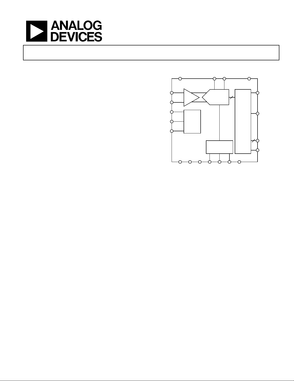
FUNCTIONAL BLOCK DIAGRAM
VDD DRVDD
AD9244
VIN+
VIN–
CLK+
CLK–
DCS
SHA
TIMING
AGND DGNDVREF SENSE
Fabricated on an advanced CMOS process, the AD9244 is
available in a 48-lead LQFP and is specified for operation over
the industrial temperature range (–40°C to +85°C).
PRODUCT HIGHLIGHTS
1. Low Power—The AD9244, at 550 mW, consumes a fraction
of the power of currently available ADCs in existing high
speed solutions.
2. IF Sampling—The AD9244 delivers outstanding
performance at input frequencies beyond the first Nyquist
zone. Sampling at 65 MSPS with an input frequency of
100 MHz, the AD9244 delivers 71 dB SNR and 86 dB SFDR.
3. Pin Compatibility—The AD9244 offers a seamless
migration from the 12-bit, 65 MSPS
4. On-Board Sample-and-Hold (SHA)—The versatile SHA
input can be configured for either single-ended or
differential inputs.
5. Out-of-Range (OTR) Indicator—The OTR output bit
indicates when the input signal is beyond the AD9244’s
input range.
6. Single Supply—The AD9244 uses a single 5 V power
supply, simplifying system power supply design. It also
features a separate digital output driver supply to
accommodate 3.3 V and 5 V logic families.
VRCML
REFT REFB
10-STAGE
PIPELINE ADC
REFERENCE
Figure 1.
14
REF
GND
AD9226.
OUTPUT
REGISTER
14
DFS
OTR
D13 TO D0
OEB
02404-001
Rev. C
Information furnished by Analog Devices is believed to be accurate and reliable. However, no
responsibility is assumed by Anal og Devices for its use, nor for any infringements of patents or ot her
rights of third parties that may result from its use. Specifications subject to change without notice. No
license is granted by implication or otherwise under any patent or patent rights of Analog Devices.
Trademarks and registered trademarks are the property of their respective owners.
One Technology Way, P.O. Box 9106, Norwood, MA 02062-9106, U.S.A.
Tel: 781.329.4700 www.analog.com
Fax: 781.461.3113 © 2005 Analog Devices, Inc. All rights reserved.
Page 2

AD9244
TABLE OF CONTENTS
Features .............................................................................................. 1
Te r mi n ol o g y .......................................................................................9
Functional Block Diagram .............................................................. 1
Applications....................................................................................... 1
General Description......................................................................... 1
Product Highlights ........................................................................... 1
Revision History ............................................................................... 2
Specifications..................................................................................... 3
DC Specifications ......................................................................... 3
AC Specifications.......................................................................... 4
Digital Specifications ................................................................... 5
Switching Specifications .............................................................. 6
Absolute Maximum Ratings............................................................ 7
Explanation of Test Levels........................................................... 7
ESD Caution.................................................................................. 7
Pin Configuration and Function Descriptions............................. 8
REVISION HISTORY
Typical Applicat i o n C i rc uits ......................................................... 11
Typical Perf or m an c e Charac t e r istics ........................................... 12
Theory of Operation ...................................................................... 17
Analog Input and Reference Overview ................................... 17
Analog Input Operation............................................................ 18
Reference Operation .................................................................. 20
Digital Inputs and Outputs ....................................................... 21
Evaluation Board ............................................................................ 26
Analog Input Configuration..................................................... 26
Reference Configuration ........................................................... 26
Clock Configuration .................................................................. 26
Outline Dimensions ....................................................................... 36
Ordering Guide .......................................................................... 36
12/05—Rev. B to Rev. C
Updated Format..................................................................Universal
Changes to Figure 45...................................................................... 19
Added Single-Ended Input Configuration Section.................... 19
Added Reference Decoupling Section ......................................... 25
Changes to Figure 65...................................................................... 28
Changes to Figure 66...................................................................... 29
Changes to Figure 67...................................................................... 30
Added Table 15 ............................................................................... 34
2/05—Rev. A to Rev. B
Updated Format.................................................................. Universal
Changes to Table 1.............................................................................3
Changes to Table 2.............................................................................4
Reformatted Table 5 ..........................................................................7
Changes to Table 6.............................................................................8
Changes to Figure 12...................................................................... 12
Changed Captions on Figure 18 and Figure 21.......................... 13
Changes to Figure 35, Figure 38, Figure 39................................. 16
Changes to Table 9.......................................................................... 18
Changes to Table 13 ....................................................................... 26
Changes to Ordering Guide.......................................................... 36
6/03—Rev. 0 to Rev. A
Changes to AC Specifications..........................................................3
Updated Ordering Guide .................................................................6
Updated Outline Dimensions....................................................... 33
6/02—Revision 0: Initial Version
Rev. C | Page 2 of 36
Page 3

AD9244
SPECIFICATIONS
DC SPECIFICATIONS
AVDD = 5 V, DRVDD = 3 V, f
differential analog inputs, unless otherwise noted.
Table 1.
Test AD9244BST-65 AD9244BST-40
Parameter Temp Level Min Typ Max Min Typ Max Unit
RESOLUTION Full VI 14 14 Bits
DC ACCURACY
No Missing Codes Full VI Guaranteed Guaranteed Bits
Offset Error Full VI ±0.3 ±1.4 ±0.3 ±1.4 % FSR
Gain Error
Differential Nonlinearity (DNL)
25°C V ±0.7 ±0.6 LSB
Integral Nonlinearity (INL)
Full VI −4 +4 −4 +4 LSB
TEMPERATURE DRIFT
Offset Error Full V ±2.0 ±2.0 ppm/°C
Gain Error (EXT VREF)
Gain Error (INT VREF)
INTERNAL VOLTAGE REFERENCE
Output Voltage Error (2 VREF) Full VI ±29 ±29 mV
Load Regulation @ 1 mA Full V 0.5 0.5 mV
Output Voltage Error (1 VREF) Full IV ±15 ±15 mV
Load Regulation @ 0.5 mA Full V 0.25 0.25 mV
Input Resistance Full V 5 5 kΩ
INPUT REFERRED NOISE
VREF = 2 V 25°C V 0.8 0.8 LSB rms
VREF = 1 V 25°C V 1.5 1.5 LSB rms
ANALOG INPUT
Input Voltage Range (Differential)
Common-Mode Voltage Full V 0.5 4 0.5 4 V
Input Capacitance
Input Bias Current
Analog Bandwidth (Full Power) 25°C V 750 750 MHz
POWER SUPPLIES
Supply Voltages
Supply Current
POWER CONSUMPTION
DC Input
Sine Wave Input Full VI 590 640 345 370 mW
1
Gain error is based on the ADC only (with a fixed 2.0 V external reference).
2
Measured at maximum clock rate, fIN = 2.4 MHz, full-scale sine wave, with approximately 5 pF loading on each output bit.
3
Includes internal voltage reference error.
4
Input capacitance refers to the effective capacitance between one differential input pin and AGND. Refer to Figure 7 for the equivalent analog input structure.
5
Input bias current is due to the input looking like a resistor that is dependent on the clock rate.
6
Measured with dc input at maximum clock rate.
1
2
1
3
VREF = 2 V Full V 2 2 V p-p
VREF = 1 V Full V 1 1 V p-p
4
5
AVDD Full IV 4.75 5 5.25 4.75 5 5.25 V
DRVDD Full IV 2.7 5.25 2.7 5.25 V
IAVDD Full V 109 64 mA
IDRVDD Full V 12 8 mA
PSRR Full V ±0.05 ±0.05 % FSR
6
= 65 MSPS (–65) or 40 MSPS (–40), differential clock inputs, VREF = 2 V, external reference,
SAMPLE
Full VI ±0.6 ±2.0 ±0.6 ±2.0 % FSR
2
Full VI ±1.0 ±1.0 LSB
Full V ±1.4 ±1.3 LSB
Full V ±2.3 ±2.3 ppm/°C
Full V ±25 ±25 ppm/°C
25°C V 10 10 pF
25°C V 500 500 µA
Full V 550 300 mW
Rev. C | Page 3 of 36
Page 4

AD9244
AC SPECIFICATIONS
AVDD = 5 V, DRVDD = 3 V, f
A
= –0.5 dBFS, differential analog inputs, unless otherwise noted.
IN
Table 2.
Test AD9244BST-65 AD9244BST-40
Parameter Temp Level Min Typ Max Min Typ Max Unit
1
SNR
fIN = 2.4 MHz Full VI 72.4 73.4 dBc
25°C I 74.8 75.3 dBc
fIN = 15.5 MHz (–1 dBFS) Full IV 72.0 dBc
25°C V 73.7 dBc
fIN = 20 MHz Full VI 72.1 dBc
25°C I 74.7 dBc
fIN = 32.5 MHz Full IV 70.8 dBc
25°C I 73.0 dBc
fIN = 70 MHz Full IV 69.9 dBc
25°C V 72.2 dBc
fIN = 100 MHz 25°C V 71.2 72.8 dBc
fIN = 200 MHz 25°C V 67.2 68.3 dBc
1
SINAD
fIN = 2.4 MHz Full VI 72.2 73.2 dBc
25°C I 74.7 75.1 dBc
fIN = 20 MHz Full VI 72 dBc
25°C I 74.4 dBc
fIN = 32.5 MHz Full IV 70.6 dBc
25°C I 72.6 dBc
fIN = 70 MHz Full IV 69.7 dBc
25°C V 71.9 dBc
fIN = 100 MHz 25°C V 71 72.4 dBc
fIN = 200 MHz 25°C V 59.8 56.3 dBc
ENOB
fIN = 2.4 MHz Full VI 11.7 11.9 Bits
25°C I 12.1 12.2 Bits
fIN = 20 MHz Full VI 11.7 Bits
25°C I 12.1 Bits
fIN = 32.5 MHz Full IV 11.4 Bits
25°C I 11.8 Bits
fIN = 70 MHz Full IV 11.3 Bits
25°C V 11.7 Bits
fIN = 100 MHz 25°C V 11.5 11.7 Bits
fIN = 200 MHz 25°C V 9.6 9.1 Bits
1
THD
fIN = 2.4 MHz Full VI −78.4 −80.7 dBc
25°C I −90.0 −89.7 dBc
fIN = 20 MHz Full VI −80.4 dBc
25°C I −89.4 dBc
fIN = 32.5 MHz Full IV −79.2 dBc
25°C I −84.6 dBc
fIN = 70 MHz Full IV −78.7 dBc
25°C V −84.1 dBc
fIN = 100 MHz 25°C V −83.0 −83.2 dBc
fIN = 200 MHz 25°C V −60.7 −56.6 dBc
= 65 MSPS (–65) or 40 MSPS (–40), differential clock inputs, VREF = 2 V, external reference,
SAMPLE
Rev. C | Page 4 of 36
Page 5

AD9244
Test AD9244BST-65 AD9244BST-40
Parameter Temp Level Min Typ Max Min Typ Max Unit
WORST HARMONIC (SECOND or THIRD)
fIN = 2.4 MHz 25°C V −94.5 −93.7 dBc
fIN = 20 MHz 25°C V −92.8 dBc
fIN = 32.5 MHz 25°C V −86.5 dBc
fIN = 70 MHz 25°C V −86.1 dBc
fIN = 100 MHz 25°C V −86.2 −84.5 dBc
fIN = 200 MHz 25°C V −60.7 −56.6 dBc
1
SFDR
fIN = 2.4 MHz Full VI 78.6 82.5 dBc
25°C I 94.5 93.7 dBc
fIN = 15.5 MHz (–1 dBFS) Full IV 83 dBc
25°C V 90 dBc
fIN = 20 MHz Full IV 81.4 dBc
25°C I 91.8 dBc
fIN = 32.5 MHz Full IV 80.0 dBc
25°C I 86.4 dBc
fIN = 70 MHz Full IV 79.5 dBc
25°C V 86.1 dBc
fIN = 100 MHz 25°C V 86.2 84.5 dBc
fIN = 200 MHz 25°C V 60.7 56.6 dBc
1
AC specifications can be reported in dBc (degrades as signal levels are lowered) or in dBFS (always related back to converter full scale).
DIGITAL SPECIFICATIONS
AVDD = 5 V, DRVDD = 3 V, VREF = 2 V, external reference, unless otherwise noted.
Table 3.
Test AD9244BST-65 AD9244BST-40
Parameter Temp Level Min Typ Max Min Typ Max Unit
DIGITAL INPUTS
Logic 1 Voltage (OEB, DRVDD = 3 V) Full IV 2 2 V
Logic 1 Voltage (OEB, DRVDD = 5 V) Full IV 3.5 3.5 V
Logic 0 Voltage (OEB) Full IV 0.8 0.8 V
Logic 1 Voltage (DFS, DCS) Full IV 3.5 3.5 V
Logic 0 Voltage (DFS, DCS) Full IV 0.8 0.8 V
Input Current Full IV 10 10 µA
Input Capacitance Full V 5 5 pF
CLOCK INPUT PARAMETERS
Differential Input Voltage Full IV 0.4 0.4 V p-p
CLK− Voltage
Internal Clock Common-Mode Full V 1.6 1.6 V
Single-Ended Input Voltage
Logic 1 Voltage Full IV 2 2 V
Logic 0 Voltage Full IV 0.8 0.8 V
Input Capacitance Full V 5 5 pF
Input Resistance Full V 100 100 kΩ
DIGITAL OUTPUTS (DRVDD = 5 V)
Logic 1 Voltage (IOH = 50 µA) Full IV 4.5 4.5 V
Logic 0 Voltage (IOL = 50 µA) Full IV 0.1 0.1 V
Logic 1 Voltage (IOH = 0.5 mA) Full IV 2.4 2.4 V
Logic 0 Voltage (IOL = 1.6 mA) Full IV 0.4 0.4 V
1
1
Full IV 0.25 0.25 V
Rev. C | Page 5 of 36
Page 6
AD9244
Test AD9244BST-65 AD9244BST-40
Parameter Temp Level Min Typ Max Min Typ Max Unit
DIGITAL OUTPUTS (DRVDD = 3 V)
Logic 1 Voltage (IOH = 50 µA) Full IV 2.95 2.95 V
Logic 0 Voltage (IOL = 50 µA) Full IV 0.05 0.05 V
Logic 1 Voltage (IOH = 0.5 mA) Full IV 2.8 2.8 V
Logic 0 Voltage (IOL = 1.6 mA) Full IV 0.4 0.4 V
1
See the Clock Overview section for more details.
2
Output voltage levels measured with 5 pF load on each output.
SWITCHING SPECIFICATIONS
AVDD = 5 V, DRVDD = 3 V, unless otherwise noted.
Table 4.
Test AD9244BST-65 AD9244BST-40
Parameter Temp Level Min Typ Max Min Typ Max Unit
CLOCK INPUT PARAMETERS
Maximum Conversion Rate Full VI 65 40 MHz
Minimum Conversion Rate Full V 500 500 kHz
Clock Period
Clock Pulse Width High
Clock Pulse Width Low
Clock Pulse Width High
Clock Pulse Width Low
DATA OUTPUT PARAMETERS
Output Delay (tPD)
Pipeline Delay (Latency) Full V 8 8 Clock cycles
Aperture Delay (tA) Full V 1.5 1.5 ns
Aperture Uncertainty (Jitter) Full V 0.3 0.3 ps rms
Output Enable Delay Full V 15 15 ns
OUT-OF-RANGE RECOVERY TIME Full V 2 1 Clock cycles
1
The clock period can be extended to 2 µs with no degradation in specified performance at 25°C.
2
With duty cycle stabilizer enabled.
3
With duty cycle stabilizer disabled.
4
Measured from clock 50% transition to data 50% transition with 5 pF load on each output.
1
2
3
4
2
Full V 15.4 25 ns
2
Full V 4 4 ns
Full V 4 4 ns
3
Full V 6.9 11.3 ns
Full V 6.9 11.3 ns
Full V 3.5 7 3.5 7 ns
ANALOG INPUT
CLOCK
DATA OUT
N + 2
N + 1
N
t
A
N – 9 N – 8 N – 7 N – 6 N – 5 N – 4 N – 3 N – 2 N – 1 N N + 1
N + 3
N + 4
N + 5
N + 6
N + 7
N + 8
N + 9
t
PD
Figure 2. Input Timing
Rev. C | Page 6 of 36
02404-002
Page 7

AD9244
ABSOLUTE MAXIMUM RATINGS
Table 5.
With
Parameter
ELECTRICAL
AVDD AGND –0.3 V to +6.5 V
DRVDD DGND −0.3 V to +6.5 V
AGND DGND –0.3 V to +0.3 V
AVDD DRVDD –6.5 V to +6.5 V
REFGND AGND –0.3 V to +0.3 V
CLK+, CLK–, DCS AGND –0.3 V to AVDD + 0.3 V
DFS AGND –0.3 V to AVDD + 0.3 V
VIN+, VIN– AGND –0.3 V to AVDD + 0.3 V
VREF AGND –0.3 V to AVDD + 0.3 V
SENSE AGND –0.3 V to AVDD + 0.3 V
REFB, REFT AGND –0.3 V to AVDD + 0.3 V
CML AGND –0.3 V to AVDD + 0.3 V
VR AGND –0.3 V to AVDD + 0.3 V
OTR DGND –0.3 V to DRVDD + 0.3 V
D0 to D13 DGND –0.3 V to DRVDD + 0.3 V
OEB DGND –0.3 V to DRVDD + 0.3 V
ENVIRONMENTAL
Junction Temperature 150°C
Storage Temperature −65°C to +150°C
Operating Temperature −40°C to +85°C
Lead Temperature (10 sec) 300°C
1
Typical thermal impedances; θJA = 50.0°C/W; θJC = 17.0°C/W. These
measurements were taken on a 4-layer board in still air, in accordance with
EIA/JESD51-7.
Respect to
1
Rating
Stresses above those listed under Absolute Maximum Ratings
may cause permanent damage to the device. This is a stress
rating only; functional operation of the device at these or any
other conditions above those indicated in the operational
sections of this specification is not implied. Exposure to
absolute maximum ratings for extended periods may affect
device reliability.
EXPLANATION OF TEST LEVELS
Table 6.
Te st
Level
I 100% production tested.
II
III Sample tested only.
IV
V Parameter is a typical value only.
VI
Description
100% production tested at 25°C and sample tested at
specified temperatures.
Parameter is guaranteed by design and characterization
testing.
100% production tested at 25°C; guaranteed by design
and characterization testing for industrial temperature
range; 100% production tested at temperature extremes
for military devices.
ESD CAUTION
ESD (electrostatic discharge) sensitive device. Electrostatic charges as high as 4000 V readily accumulate on the
human body and test equipment and can discharge without detection. Although this product features
proprietary ESD protection circuitry, permanent damage may occur on devices subjected to high energy
electrostatic discharges. Therefore, proper ESD precautions are recommended to avoid performance
degradation or loss of functionality.
Rev. C | Page 7 of 36
Page 8
AD9244
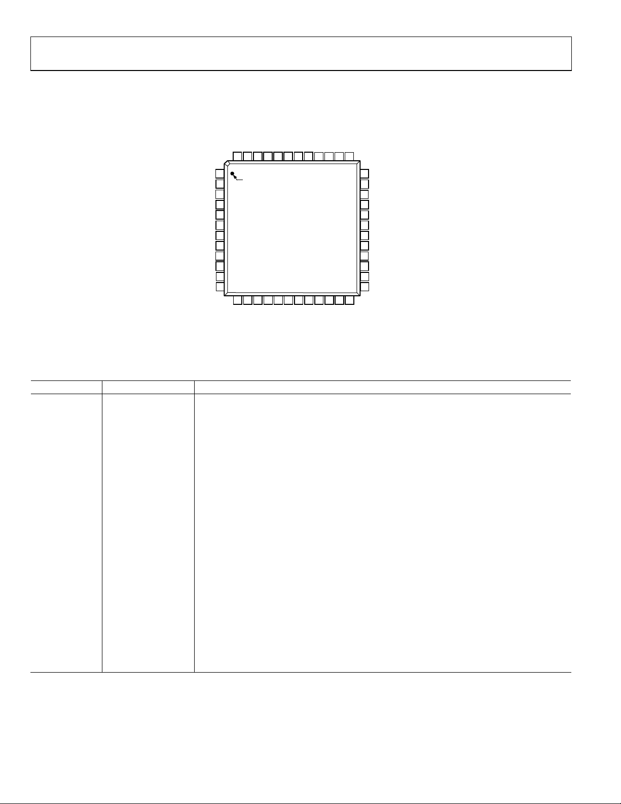
PIN CONFIGURATION AND FUNCTION DESCRIPTIONS
VIN–46VIN+45CML44NIC43DCS42REFT41REFT40REFB39REFB38REFGND37VREF
48VR47
23
DGND
DRVDD
36
SENSE
35
DFS
34
AVDD
33
AGND
32
AGND
31
AVDD
30
DGND
29
DRVDD
28
OTR
27
D13 (MSB)
26
D12
25
D11
24
D10
02404-003
AGND
AGND
AVDD
AVDD
AGND
CLK–
CLK+
NIC
OEB
D0 (LSB)
1
PIN 1
2
3
4
5
6
7
8
9
10
11
D1
12
D2
13D314
AD9244
TOP VIEW
(Not to Scale)
15
16D417D518D619D720D821D922
DGND
DRVDD
Figure 3. Pin Configuration
Table 7. Pin Function Descriptions
Pin No. Mnemonic Description
1, 2, 5, 32, 33 AGND Analog Ground.
3, 4, 31, 34 AVDD Analog Supply Voltage.
6, 7 CLK–, CLK+ Differential Clock Inputs.
8, 44 NIC No Internal Connection.
9 OEB Digital Output Enable (Active Low).
10 D0 (LSB) Least Significant Bit, Digital Output.
11 to 13,
16 to 21,
24 to 26
D1 to D3,
D4 to D9,
D10 to D12
Digital Outputs.
14, 22, 30 DGND Digital Ground.
15, 23, 29 DRVDD Digital Supply Voltage.
27 D13 (MSB) Most Significant Bit, Digital Output.
28 OTR Out-of-Range Indicator (Logic 1 Indicates OTR).
35 DFS Data Format Select. Connect to AGND for straight binary, AVDD for twos complement.
36 SENSE Internal Reference Control.
37 VREF Internal Reference.
38 REFGND Reference Ground.
39 to 42 REFB, REFT Internal Reference Decoupling.
43 DCS
50% Duty Cycle Stabilizer. Connect to AVDD to activate 50% duty cycle stabilizer, AGND for
external control of both clock edges.
45 CML Common-Mode Reference (0.5 × AVDD).
46, 47 VIN+, VIN– Differential Analog Inputs.
48 VR Internal Bias Decoupling.
Rev. C | Page 8 of 36
Page 9

AD9244
TERMINOLOGY
Analog Bandwidth (Full Power Bandwidth)
The analog input frequency at which the spectral power of the
fundamental frequency (as determined by the FFT analysis) is
reduced by 3 dB.
Aperture Delay
The delay between the 50% point of the rising edge of the clock
and the instant at which the analog input is sampled.
Aperture Uncertainty (Jitter)
The sample-to-sample variation in aperture delay.
Differential Analog Input Voltage Range
The peak-to-peak differential voltage must be applied to the
converter to generate a full-scale response. Peak differential
voltage is computed by observing the voltage on a single pin
and subtracting the voltage from the other pin, which is 180°
out of phase. Peak-to-peak differential is computed by rotating
the input phase 180° and taking the peak measurement again. The
difference is then found between the two peak measurements.
Differential Nonlinearity (DNL, No Missing Codes)
An ideal ADC exhibits code transitions that are exactly 1 LSB
apart. DNL is the deviation from this ideal value. Guaranteed
no missing codes to 14-bit resolution indicates that all 16,384
codes must be present over all operating ranges.
Dual-Tone SFDR
1
The ratio of the rms value of either input tone to the rms value
of the peak spurious component. The peak spurious component
may or may not be an IMD product.
Effective Number of Bits (ENOB)
The ENOB for a device for sine wave inputs at a given input
frequency can be calculated directly from its measured SINAD by
N = (SINAD − 1.76)/6.02
Gain Error
The first code transition should occur at an analog value ½ LSB
above negative full scale. The last code transition should occur
at an analog value 1½ LSB below the nominal full scale. Gain
error is the deviation of the actual difference between first and
last code transitions and the ideal difference between first and
last code transitions.
Common-Mode Rejection Ratio (CMRR)
Common-mode (CM) signals appearing on VIN+ and VIN–
are ideally rejected by the differential front end of the ADC.
With a full-scale CM signal driving both VIN+ and VIN–,
CMRR is the ratio of the amplitude of the full-scale input CM
signal to the amplitude of signal that is not rejected, expressed
in dBFS.
1
IF Sampling
Due to the effects of aliasing, an ADC is not necessarily limited
to Nyquist sampling. Higher sampled frequencies are aliased
down into the first Nyquist zone (DC − f
/2) on the output
CLOCK
of the ADC. Care must be taken that the bandwidth of the sampled signal does not overlap Nyquist zones and alias onto itself.
Nyquist sampling performance is limited by the bandwidth of
the input SHA and clock jitter (noise caused by jitter increases
as the input frequency increases).
Integral Nonlinearity (INL)
INL refers to the deviation of each individual code from a line
drawn from negative full scale through positive full scale. The
point used as negative full scale occurs ½ LSB before the first
code transition. Positive full scale is defined as a level 1½ LSB
beyond the last code transition. The deviation is measured from
the middle of each particular code to the true straight line.
Minimum Conversion Rate
The clock rate at which the SNR of the lowest analog signal
frequency drops by no more than 3 dB below the guaranteed limit.
Maximum Conversion Rate
The clock rate at which parametric testing is performed.
Nyquist Sampling
When the frequency components of the analog input are below
the Nyquist frequency (f
CLOCK
/2).
Out-of-Range Recovery Time
The time it takes for the ADC to reacquire the analog input
after a transition from 10% above positive full scale to 10%
above negative full scale, or from 10% below negative full scale
to 10% below positive full scale.
Power Supply Rejection Ratio (PSRR)
The change in full scale from the value with the supply at its
minimum limit to the value with the supply at its maximum limit.
Signal-to-Noise-and-Distortion (SINAD)
1
TThe ratio of the rms signal amplitude to the rms value of the
sum of all other spectral components below the Nyquist
frequency, including harmonics, but excluding dc.
Signal-to-Noise Ratio (SNR)
1
The ratio of the rms signal amplitude to the rms value of the
sum of all other spectral components below the Nyquist
frequency, excluding the first six harmonics and dc.
Rev. C | Page 9 of 36
Page 10

AD9244
Spurious-Free Dynamic Range (SFDR)
1
The difference in dB between the rms amplitude of the input
signal and the peak spurious signal.
Total Harmonic Distortion (THD)
The ratio of the rms sum of the first six harmonic components
to the rms value of the measured input signal.
1
Tem p er at u re Dr i ft
The temperature drift for offset error and gain error specifies
the maximum change from initial (25°C) value to the value at
T
MIN
or T
MAX
.
Offset Error
The major carry transition should occur for an analog value
½ LSB below VIN+ = VIN−. Offset error is defined as the
deviation of the actual transition from that point.
1
AC specifications can be reported in dBc (degrades as signal levels are
lowered) or in dBFS (always related back to converter full scale).
Rev. C | Page 10 of 36
Page 11
AD9244
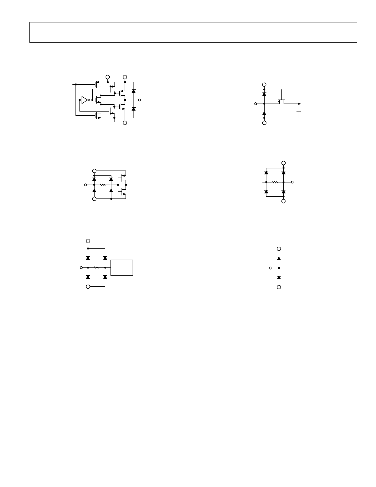
TYPICAL APPLICATION CIRCUITS
DRVDD DRVDD
AVDD
DGND
Figure 4. D0 to D13, OTR
DRVDD
200Ω
DGND
Figure 5. Three-State (OEB)
AVDD
200Ω
AGND
CLK
BUFFER
Figure 6. CLK+, CLK−
02404-005
02404-006
02404-004
AGND
02404-007
Figure 7. VIN+, VIN−
AVDD
200Ω
AGND
02404-008
Figure 8. DFS, DCS, SENSE
AVDD
AGND
02404-009
Figure 9. VREF, REFT, REFB, VR, CML
Rev. C | Page 11 of 36
Page 12

AD9244
TYPICAL PERFORMANCE CHARACTERISTICS
AVDD = 5.0 V, DRVDD = 3.0 V, f
mode voltage (V
0
–20
) = 2.5 V, input amplitude (AIN) = −0.5 dBFS, VREF = 2.0 V external, FFT length = 8K, unless otherwise noted.
CM
= 65 MSPS with CLK duty cycle stabilizer enabled, TA = 25°C, differential analog input, common-
SAMPLE
SNR = 74.8dBc
SFDR = 93.6dBc
100
90
SFDR (dBFS)
AMPLITUDE (dBFS)
AMPLITUDE (dBFS)
–40
–60
–80
–100
–120
0
–20
–40
–60
–80
–100
Figure 10. Single-Tone FFT, f
SNR = 74.0dBc
SFDR = 87.0dBc
FREQUENCY (MHz)
= 5 MHz
IN
32.50105 15202530
02404-010
80
70
60
50
40
SFDR = 90dBc
REFERENCE LINE
dBFS AND dBc
Figure 13. Single-Tone SNR/SFDR vs. A
100
SFDR (dBFS)
90
80
SNR (dBFS)
SFDR (dBc)
70
60
50
SFDR = 90dBc
REFERENCE LINE
SNR (dBc)
dBFS AND dBc
SFDR (dBc)
AIN (dBFS)
SNR (dBFS)
SNR (dBc)
, fIN = 5 MHz
IN
0–30 –25 –20 –15 –10 –5
02404-013
–120
FREQUENCY (MHz)
Figure 11. Single-Tone FFT, f
= 31 MHz
IN
0
SFDR = 74.0dBc
–20
–40
–60
–80
AMPLITUDE (dBFS)
–100
–120
0 5 10 15 20 25 30
Figure 12. Single-Tone FFT, fIN = 190 MHz, f
FREQUENCY (MHz)
SAMPLE
SNR = 66.5dBc
= 61.44 MSPS
32.50 10.05.0 15.0 20.0 25.0 30.0
02404-011
02404-012
Rev. C | Page 12 of 36
40
AIN (dBFS)
Figure 14. Single-Tone SNR/SFDR vs. A
100
90
80
SNR (dBFS)
SFDR (dBc)
70
dBFS AND dBc
60
50
40
SFDR = 90dBc
REFERENCE LINE
SNR (dBc)
AIN (dBFS)
Figure 15. Single-Tone SNR/SFDR vs. A
SFDR (dBFS)
, fIN = 190 MHz, f
IN
, fIN = 31 MHz
IN
SAMPLE
030 –25 –20 –15 –10 –5
02404-014
0–30 –25 –20 –15 –10 –5
02404-015
= 61.44 MSPS
Page 13

AD9244
75
12.2
75
73
71
2V SPAN
69
SINAD (dBc)
67
65
INPUT FREQUENCY (MHz)
1V SPAN
11.9
11.5
11.2
ENOB (Bits)
10.8
10.5
1400 20406080100120
02404-016
Figure 16. SINAD/ENOB vs. Input Frequency
–100
–95
–90
–85
THD (dBc)
–80
1V SPAN
2V SPAN
73
71
69
SNR (dBc)
67
65
INPUT FREQUENCY (MHz)
2V SPAN
1V SPAN
1400 20 40 60 80 100 120
02404-019
Figure 19. SNR vs. Input Frequency
100
95
90
85
SFDR (dBc)
80
1V SPAN
2V SPAN
–75
INPUT FREQUENCY (MHz)
1400 20 40 60 80 100 120
Figure 17. THD vs. Input Frequency
77
75
+25°C
73
–40°C
71
SNR (dBc)
69
+85°C
67
INPUT FREQUENCY (MHz)
1400 20 40 60 80 100 120
Figure 18. SNR vs. Temperature and Input Frequency, DCS Disabled
02404-017
02404-018
75
INPUT FREQUENCY (MHz)
1400 20 40 60 80 100 120
Figure 20. SFDR vs. Input Frequency
–92
–90
–88
–86
–84
–82
THD (dBc)
–80
–78
–76
–74
+25°C
+85°C
INPUT FREQUENCY (MHz)
–40°C
1400 20 40 60 80 100 120
Figure 21. THD vs. Temperature and Input Frequency, DCS Disabled
02404-020
02404-021
Rev. C | Page 13 of 36
Page 14

AD9244
–100
100
FOURTH
–95
–90
–85
HARMONICS (dBc)
–80
–75
INPUT FREQUENCY (MHz)
HARMONIC
THIRD
HARMONIC
SECOND
HARMONIC
1400 20 40 60 80 100 120
02404-022
Figure 22. Harmonics vs. Input Frequency
76
75
74
f
= 10MHz
f
= 20MHz
IN
IN
73
SINAD (dBc)
72
71
f
= 2MHz
IN
12.33
12.17
12.00
11.83
11.67
11.50
ENOB (Bits)
95
90
85
80
75
SNR/SFDR (dBc)
60
65
60
DUTY CYCLE (%)
Figure 25. SNR/SFDR vs. Duty Cycle, f
SFDR, DCS ON
SFDR, DCS OFF
SNR, DCS ON
SNR, DCS OFF
= 2.5 MHz
IN
7030 35 40 45 50 55 60 65
02404-025
100
f
= 2MHz
IN
96
92
88
SFDR (dBc)
f
84
IN
= 20MHz
f
= 10MHz
IN
INL (LSB)
70
–0.5
–1.0
–1.5
1.5
1.0
0.5
SAMPE RATE (MSPS)
Figure 23. SINAD/ENOB vs. Sample Rate
0
CODES (14-Bit)
Figure 24. Typical INL
11.34
1000 20406080
02404-023
80
SAMPLE RATE (MSPS)
1000 20406080
02404-026
Figure 26. SFDR vs. Sample Rate
1.0
0.8
0.6
0.4
0.2
0
–0.2
DNL (LSB)
–0.4
–0.6
–0.8
163840 4096 8192 12288
02404-024
–1.0
CODES (14-Bit)
163840 4096 8192 12288
02404-027
Figure 27. Typical DNL
Rev. C | Page 14 of 36
Page 15

AD9244
–20
–40
0
SNR = 67.5dBc
SFDR = 93.2dBc
100
SFDR (dBFS)
90
SFDR (dBc)
80
–60
–80
AMPLITUDE (dBFS)
–100
–120
Figure 28. Dual-Tone FFT with f
= 45.6 MHz (A
f
IN−2
0
20
40
60
80
AMPLITUDE (dBFS)
100
120
Figure 29. Dual-Tone FFT with f
= 70.6 MHz (A
f
IN−2
0
–20
FREQUENCY (MHz)
IN−1
= A
= –6.5 dBFS)
IN1
IN2
FREQUENCY (MHz)
iN−1
= A
= –6.5 dBFS)
IN1
IN2
= 44.2 MHz and
SNR = 67.0dBc
SFDR = 78.2dBc
3
= 69.2 MHz and
SNR = 65.0dBc
SFDR = 69.1dBc
70
dBFS AND dBc
60
50
32.50 10.05.0 20.015.0 25.0 30.0
02404-028
40
SFDR = 90dBc
REFERENCE LINE
SNR (dBc)
AIN (dBFS)
Figure 31. Dual-Tone SNR/SFDR vs. A
= 44.2 MHz and f
f
IN−1
IN−2
SNR (dBFS)
IN
= 45.6 MHz
with
–5–30 –25 –20 –15 –10
02404-031
100
SFDR (dBFS)
90
80
SNR (dBFS)
70
SFDR (dBc)
SFDR = 90dBc
dBFS AND dBc
60
50
0
.
32.50 10.05.0 25.020.015.0
0
02404-029
40
REFERENCE LINE
SNR (dBc)
AIN (dBFS)
Figure 32. Dual-Tone SNR/SFDR vs. A
= 69.2 MHz and= f
f
IN−1
= 70.6 MHz
IN−2
with
IN
–5–30 –25 –20 –15 –10
02404-032
100
SFDR (dBFS)
90
–40
–60
–80
AMPLITUDE (dBFS)
–100
–120
Figure 30. Dual-Tone FFT with f
= 140.7 MHz (A
f
IN−2
FREQUENCY (MHz)
IN−1
= A
= –6.5 dBFS)
IN1
IN2
= 139.2 MHz and
32.50 5.0 10.0 15.0 20.0 25.0 30.0
02404-030
Rev. C | Page 15 of 36
80
70
dBFS AND dBc
60
50
40
SNR (dBFS)
SFDR (dBc)
SFDR = 90dBc
REFERENCE LINE
SNR (dBc)
AIN (dBFS)
Figure 33. Dual-Tone SNR/SFDR vs. A
= 139.2 MHz and f
f
IN−1
= 140.7 MHz
IN−2
with
IN
–5–30 –25 –20 –15 –10
02404-033
Page 16

AD9244
–20
0
SNR = 62.6dBc
SFDR = 60.7dBc
100
90
SFDR (dBFS)
–40
–60
–80
AMPLITUDE (dBFS)
–100
–120
FREQUENCY (MHz)
Figure 34. Dual-Tone with f
= 240.7 MHz (A
f
IN−2
IN−1
= A
IN−1
IN−2
= 239.1 MHz and
= –6.5 dBFS)
0
–10
–20
–30
–40
–50
–60
NOTE: SPUR FLOOR
–70
BELOW 90dBFS @ 240MHz
–80
AMPLITUDE (dBFS)
–90
–100
–110
–120
0 5 10 15 20 25 30
FREQUENCY (MHz)
SNR = 71.3dBc
THD = –90.8dBc
Figure 35. Driving ADC Inputs with Transformer and Balun,
= 240 MHz, AIN = –8.5 dBFS
f
IN
105
100
80
SNR (dBFS)
70
SFDR (dBc)
dBFS AND dBc
60
SFDR = 90dBc
REFERENCE LINE
50
32.505 25201510 30.0
02404-034
40
SNR (dBc)
AIN (dBFS)
Figure 37. Dual-Tone SNR/SFDR vs. A
= 239.1 MHz and f
f
IN−1
= 240.7 MHz
IN−2
with
IN
–5–30 –25 –20 –15 –10
02404-037
100
95
02404-035
90
85
80
75
70
dBFS AND dBc
65
60
55
50
SFDR (dBFS)
SFDR (dBc)
SNR (dBFS)
SNR (dBc)
AIN (dBFS)
SFDR = 90dBc
REFERENCE LINE
0–21 –18 –15 –12 –9 –6 –3
02404-038
Figure 38. Driving ADC Inputs with Transformer and
Balun SNR/SFDR vs. A
, fIN = 240 MHz
IN
95
90
SFDR (dBFS)
95
90
85
80
AMPLITUDE (dBFS)
75
70
65
INPUT FREQUENCY (MHz)
Figure 36. CMRR vs. Input Frequency (A
= 0 dBFS and CML = 2.5 V)
IN
2500 50 100 150 200
02404-036
Rev. C | Page 16 of 36
85
80
75
70
dBFS AND dBc
65
60
55
SFDR (dBc)
SNR (dBFS)
SNR (dBc)
AIN (dBFS)
Figure 39. Driving ADC Inputs with Transformer and
Balun SNR/SFDR vs. A
, fIN = 190 MHz
IN
SFDR = 90dBc
REFERENCE LINE
0–21 –18 –15 –12 –9 –6 –3
02404-039
Page 17

AD9244
2
3
2
V
V
THEORY OF OPERATION
The AD9244 is a high performance, single-supply 14-bit ADC.
In addition to high dynamic range Nyquist sampling, it is
designed for excellent IF undersampling performance with an
analog input as high as 240 MHz.
The AD9244 uses a calibrated 10-stage pipeline architecture
with a patented, wideband, input sample-and-hold amplifier
(SHA) implemented on a cost-effective CMOS process. Each
stage of the pipeline, excluding the last, consists of a low resolution flash ADC along with a switched capacitor DAC and
interstage residue amplifier (MDAC). The MDAC amplifies the
difference between the reconstructed DAC output and the flash
input for the next stage in the pipeline. One bit of redundancy is
used in each of the stages to facilitate digital correction of flash
errors. The last stage simply consists of a flash ADC.
The pipeline architecture allows a greater throughput rate at the
expense of pipeline delay or latency. While the converter captures a new input sample every clock cycle, it takes eight clock
cycles for the conversion to be fully processed and appear at the
output, as illustrated in
Figure 2. This latency is not a concern
in many applications. The digital output, together with the OTR
indicator, is latched into an output buffer to drive the output
pins. The output drivers of the AD9244 can be configured to
interface with 5 V or 3.3 V logic families.
The AD9244 has a duty clock stabilizer (DCS) that generates its
own internal falling edge to create an internal 50% duty cycle
clock, independent of the externally applied duty cycle. Control
of straight binary or twos complement output format is accomplished with the DFS pin.
The ADC samples the analog input on the rising edge of the
clock. While the clock is low, the input SHA is in sample mode.
When the clock transitions to a high logic level, the SHA goes
into the hold mode. System disturbances just prior to or immediately after the rising edge of the clock and/or excessive clock
jitter can cause the SHA to acquire the wrong input value and
should be minimized.
ANALOG INPUT AND REFERENCE OVERVIEW
The differential input span of the AD9244 is equal to the potential at the VREF pin. The VREF potential can be obtained from
the internal AD9244 reference or an external source.
In differential applications, the center point of the input span is
the common-mode level of the input signals. In single-ended
applications, the center point is the dc potential applied to one
input pin while the signal is applied to the opposite input pin.
Figure 40 to Figure 42 show various system configurations.
2.5V
.5V
1.5V
1.5V
50V
33Ω
+
10μF 0.1μ F
33Ω
20pF
AD9244
VIN+
REFT
VIN–
2V
VREF
REFB
SENSE
REFGND
0.1μF
0.1μF
0.1μF
+
10μF
Figure 40. 2 V p-p Differential Input, Common-Mode Voltage = 2 V
3.0V
2.0V
+
10μF 0.1μF
33Ω
20pF
33Ω
AD9244
VIN+
REFT
VIN–
2V
VREF
REFB
SENSE
REFGND
0.1μF
0.1μF
0.1μF
+
10μF
02404-041
Figure 41. 2 V p-p Single-Ended Input, Common-Mode Voltage = 2 V
AD9244
0.1pF
20pF
2.5V
2V
VIN+
VIN–
VREF
SENSE
REFGND
REFT
REFB
0.1μF
0.1μF
0.1μF
+
10μF
.0V
.0V
3.0V
2.0V
50Ω
33Ω
33Ω
+
10μF 0.1μ F
Figure 42. 2 V p-p Differential Input, Common-Mode Voltage = 2.5 V
Figure 43 is a simplified model of the AD9244 analog input,
showing the relationship between the analog inputs, VIN+,
VIN–, and the reference voltage, VREF. Note that this is only a
symbolic model and that no actual negative voltages exist inside
the AD9244. Similar to the voltages applied to the top and bottom of the resistor ladder in a flash ADC, the value VREF/2
defines the minimum and maximum input voltages to the
ADC core.
AD9244
IN+
IN–
V
+
–
Figure 43. Equivalent Analog Input of AD9244
CORE
+VREF/2
ADC
CORE
–VREF/2
14
02404-043
02404-040
02404-042
Rev. C | Page 17 of 36
Page 18

AD9244
A differential input structure allows the user to easily configure the
inputs for either single-ended or differential operation. The ADC’s
input structure allows the dc offset of the input signal to be varied
independent of the input span of the converter. Specifically, the
input to the ADC core can be defined as the difference of the
voltages applied at the VIN+ and VIN– input pins.
Therefore, the equation
V
= (VIN+) – (VIN−) (1)
CORE
defines the output of the differential input stage and provides
the input to the ADC core. The voltage, V
, must satisfy the
CORE
condition
−VREF/2 < V
< VREF/2 (2)
CORE
where VREF is the voltage at the VREF pin.
In addition to the limitations placed on the input voltages VIN+
and VIN– by Equation 1 and Equation 2, boundaries on the
inputs also exist based on the power supply voltages according
to the conditions
AGND − 0.3 V < VIN+ < AVDD + 0.3 V (3)
AGND − 0.3 V < VIN− < AVDD + 0.3 V (4)
The range of valid inputs for VIN+ and VIN− is any combination
that satisfies Equation 2, Equation 3, and Equation 4.
For additional information showing the relationship between
VIN+, VIN–, VREF, and the analog input range of the AD9244,
Tabl e 8 and Ta b le 9 .
see
ANALOG INPUT OPERATION
Figure 44 shows the equivalent analog input of the AD9244,
which consists of a 750 MHz differential SHA. The differential
input structure of the SHA is flexible, allowing the device to be
configured for either a differential or single-ended input. The
analog inputs VIN+ and VIN– are interchangeable, with the
exception that reversing the inputs to the VIN+ and VIN– pins
results in a data inversion (complementing the output word).
S
VIN+
VIN–
C
PIN, PAR
C
PIN, PAR
S
S
C
S
H
C
S
C
H
C
H
where:
AGND is nominally 0 V.
AVDD i s n o m in a ll y 5 V.
Figure 44. Analog Input of AD9244 SHA
S
Table 8. Analog Input Configuration Summary
Input Input Input Range (V) Input CM
Connection Coupling Span (V) VIN+
1
VIN−
1
Voltage (V) Comments
Single-Ended DC or AC 1.0 0.5 to 1.5 1.0 1.0 Best for stepped input response applications.
2.0 1 to 3 2.0 2.0
Optimum noise performance for single-ended
mode often requires low distortion op amp
with VCC > 5 V due to its headroom issues.
Differential DC or AC 1.0 2.25 to 2.75 2.75 to 2.25 2.5
Optimum full-scale THD and SFDR performance
well beyond the ADC’s Nyquist frequency.
2.0 2.0 to 3.0 3.0 to 2.0 2.5
Optimum noise performance for differential
mode. Preferred mode for applications.
1
VIN+ and VIN− can be interchanged if data inversion is required.
Table 9. Reference Configuration Summary
Reference Operating Mode Connect To Resulting VREF (V) Input Span (VIN+ − VIN−) (V p-p)
Internal SENSE VREF 1 1
Internal SENSE AGND 2 2
Internal R1 VREF and SENSE 1 ≤ VREF ≤ 2.0 1 ≤ SPAN ≤ 2
R2 SENSE and REFGND VREF = (1 + R1/R2) (SPAN = VREF)
External SENSE AVDD 1 ≤ VREF ≤ 2.0 SPAN = EXTERNAL REF
VREF EXTERNAL REF
02404-044
Rev. C | Page 18 of 36
Page 19

AD9244
V
The optimum noise and dc linearity performance for either
differential or single-ended inputs is achieved with the largest
input signal voltage span (that is, 2 V input span) and matched
input impedance for VIN+ and VIN–. Only a slight degradation
in dc linearity performance exists between the 2 V and 1 V
input spans; however, the SNR is lower in the 1 V input span.
When the ADC is driven by an op amp and a capacitive load is
switched onto the output of the op amp, the output momentarily drops due to its effective output impedance. As the output
recovers, ringing can occur. To remedy the situation, a series
resistor, R
input, as shown in
, can be inserted between the op amp and the SHA
S
Figure 45. A shunt capacitance also acts like
a charge reservoir, sinking or sourcing the additional charge
required by the sampling capacitor, C
, further reducing current
S
transients seen at the op amp’s output.
CC
V
EE
0.1μF
+
10μF
Figure 45. Resistors Isolating SHA Input from Op Amp
0.1μF
R
S
33Ω
C
20pF
R
S
5Ω
33Ω
AD9244
VIN+
S
VIN–
VREF
SENSE
REFCOM
02404-045
The optimum size of this resistor is dependent on several
factors, including the ADC sampling rate, the selected op amp,
and the particular application. In most applications, a 30 Ω to
100 Ω resistor is sufficient.
For noise-sensitive applications, the very high bandwidth of the
AD9244 can be detrimental, and the addition of a series resistor
and/or shunt capacitor can help limit the wideband noise at the
ADC’s input by forming a low-pass filter. The source impedance
driving VIN+ and VIN− should be matched. Failure to provide
matching can result in degradation of the SNR, THD, and SFDR
performance.
Single-Ended Input Configuration
A single-ended input can provide adequate performance in
cost-sensitive applications. In this configuration, there is
degradation in distortion performance due to large input
common-mode swing. However, if the source impedances on
each input are matched, there should be little effect on SNR
performance.
The internal reference can be used to drive the inputs.
Figure 45
shows an example of VREF driving VIN−. In this operating
mode, a 5 Ω resistor and a 0.1 μF capacitor must be connected
between VREF and VIN−, as shown in
Figure 45, to limit the
reference noise sampled by the analog input.
Differentially Driving the Analog Inputs
The AD9244 has a very flexible input structure, allowing it to
interface with single-ended or differential inputs.
The optimum mode of operation, analog input range, and associated interface circuitry is determined by the particular application’s
performance requirements as well as power supply options.
Differential operation requires that VIN+ and VIN− be
simultaneously driven with two equal signals that are 180°out of
phase with each other.
Differential modes of operation (ac-coupled or dc-coupled input)
provide the best SFDR performance over a wide frequency range.
They should be considered for the most demanding spectralbased applications; that is, direct IF conversion to digital.
Because not all applications have a signal precondition for
differential operation, there is often a need to perform a singleended-to-differential conversion. In systems that do not require
dc coupling, an RF transformer with a center tap is the best
method for generating differential input signals for the AD9244.
This provides the benefit of operating the ADC in the differential mode without contributing additional noise or distortion.
An RF transformer also has the added benefit of providing
electrical isolation between the signal source and the ADC.
The differential input characterization was performed using the
configuration in
Figure 46. The circuit uses a Mini-Circuits® RF
transformer, model T1-1T, which has an impedance ratio of 1:1.
This circuit assumes that the signal source has a 50 Ω source
impedance. The secondary center tap of the transformer allows
a dc common-mode voltage to be added to the differential input
signal. In
Figure 46, the center tap is connected to a resistor
divider providing a half supply voltage. It could also be
connected to the CML pin of the AD9244. For IF sampling
applications (70 MHz < f
< 200 MHz), it is recommended that
IN
the 20 pF differential capacitor between VIN+ and VIN− be
reduced or removed.
AVDD
R
S
50Ω
0.1μF
MINI-CIRCUITS
T1–1T
1kΩ
33Ω
20pF
1kΩ
R
S
33Ω
Figure 46. Transformer-Coupled Input
AD9244
VIN+
REFT
REFB
VIN–
0.1μF
0.1μF
0.1μF
+
10μF
02404-046
Rev. C | Page 19 of 36
Page 20

AD9244
The circuit in Figure 47 shows a method for applying a differential,
direct-coupled signal to the AD9244. An
AD8138 amplifier is used
to derive a differential signal from a single-ended signal.
10μF
+
μ
F
0.1
1kΩ 1kΩ
0V
1V p-p
50Ω
475Ω
499Ω
499Ω
μ
0.1
499Ω
AD8138
499Ω
5V
F
33Ω
20pF
33Ω
AVDD
VIN+
REFT
AD9244
REFB
VIN–
10μF
+
10
μ
F
0.1μF
+
0.1μF
10μF
0.1μF
Figure 47. Direct-Coupled Drive Circuit with AD8138 Differential Op Amp
REFERENCE OPERATION
The AD9244 contains a band gap reference that provides a pinstrappable option to generate either a 1 V or 2 V output. With
the addition of two external resistors, the user can generate
reference voltages between 1 V and 2 V. Another alternative is
to use an external reference for designs requiring enhanced
accuracy and/or drift performance, as described later in this
section.
voltage reference of the AD9244. A reference amplifier buffers a
1 V fixed reference. The output from the reference amplifier,
A1, appears on the VREF pin. As stated earlier, the voltage on
the VREF pin determines the full-scale differential input span
of the ADC.
The voltage appearing at the VREF pin and the state of the
internal reference amplifier, A1, are determined by the voltage
present at the SENSE pin. The logic circuitry contains comparators that monitor the voltage at the SENSE pin. The various
reference modes are summarized in
in the next few sections.
Figure 48 shows a simplified model of the internal
AD9244
TO
ADC
REFT
A2
2.5V
REFB
1V
DISABLE
A1
A1
LOGIC
VREF
R
SENSE
R
REFGND
02404-048
Figure 48. Equivalent Reference Circuit
Tabl e 9 and are described
02404-047
The actual reference voltages used by the internal circuitry of
the AD9244 appear on the REFT and REFB pins. The voltages
on these pins are symmetrical about midsupply or CML. For
proper operation, it is necessary to add a capacitor network to
decouple these pins.
Figure 49 shows the recommended
decoupling network. The turn-on time of the reference voltage
appearing between REFT and REFB is approximately 10 ms and
should be taken into consideration in any power-down mode of
operation. The VREF pin should be bypassed to the REFGND
pin with a 10 μF tantalum capacitor in parallel with a low
inductance 0.1 μF ceramic capacitor.
VREF REFT
10μF 0.1μF
1
LOCATE AS CLOSE AS POSSIBLE TO REFT/REFB PINS.
AD9244
REFGND
REFB
0.1μF110μF
Figure 49. Reference Decoupling
0.1μF
++
0.1μF
02404-049
Pin-Programmable Reference
By shorting the VREF pin directly to the SENSE pin, the internal reference amplifier is placed in a unity gain mode, and the
resulting VREF output is 1 V. By shorting the SENSE pin directly to
the REFGND pin, the internal reference amplifier is configured
for a gain of 2, and the resulting VREF output is 2 V.
Resistor-Programmable Reference
Figure 50 shows an example of how to generate a reference
voltage other than 1.0 V or 2.0 V with the addition of two
external resistors. Use the equation
VREF = 1 V × (1 + R1/R2) (5)
to determine the appropriate values for R1 and R2. These resistors
should be in the 2 kΩ to 10 kΩ range. For the example shown, R1
equals 2.5 kΩ and R2 equals 5 kΩ. From the previous equation, the
resulting reference voltage on the VREF pin is 1.5 V. This sets the
differential input span to 1.5 V p-p. The midscale voltage can also
be set to VREF by connecting VIN− to VREF.
3.25V
1.75V
+
10μF 0.1μF
2.5V
33Ω
33Ω
20pF
R1
2.5kΩ
R2
5kΩ
1.5V
Figure 50. Resistor-Programmable Reference
(1.5 V p-p Input Span, Differential Input with V
AD9244
VIN+
VIN–
VREF
SENSE
REFGND
REFT
REFB
0.1μF
0.1μF
0.1μF
= 2.5 V)
CM
+
10μF
02404-050
Rev. C | Page 20 of 36
Page 21

AD9244
V
Using an External Reference
To use an external reference, the internal reference must be disabled by connecting the SENSE pin to AVDD. The AD9244
contains an internal reference buffer, A2 (see
Figure 48), that
simplifies the drive requirements of an external reference. The
external reference must be able to drive a 5 kΩ (±20%) load.
The bandwidth of the reference is deliberately left small to
minimize the reference noise contribution. As a result, it is not
possible to drive VREF externally with high frequencies.
Figure 51 shows an example of an external reference driving
both VIN– and VREF. In this case, both the common-mode
voltage and input span are directly dependent on the value of
VREF. Both the input span and the center of the input span are
equal to the external VREF. Thus, the valid input range extends
from (VREF + VREF/2) to (VREF − VREF/2). For example, if
the Precision Reference Part
REF191, a 2.048 V external refer-
ence, is used, the input span is 2.048 V. In this case, 1 LSB of the
AD9244 corresponds to 0.125 mV.
It is essential that a minimum of a 10 μF capacitor, in parallel
with a 0.1 μF low inductance ceramic capacitor, decouple the
reference output to AGND.
Digital Outputs
Tabl e 10 details the relationship among the ADC input, OTR,
and digital output format.
Data Format Select (DFS)
The AD9244 can be programmed for straight binary or twos
complement data on the digital outputs. Connect the DFS pin to
AGND for straight binary and to AVDD for twos complement.
Digital Output Driver Considerations
The AD9244 output drivers can be configured to interface with
5 V or 3.3 V logic families by setting DRVDD to 5 V or 3.3 V,
respectively. The output drivers are sized to provide sufficient
output current to drive a wide variety of logic families.
However, large drive currents tend to cause glitches on the
supplies and can affect converter performance. Applications
requiring the ADC to drive large capacitive loads or large
fanouts can require external buffers or latches.
VREF + VREF/2
VREF – VREF/2
5
0.1μF
33Ω
20pF
VREF
Figure 51. Using an External Reference
10μF
AVDD
+
33Ω
0.1μF
AD9244
VIN+
VIN–
VREF
SENSE
REFT
REFB
0.1μF
0.1μF
0.1μF
+
10μF
02404-051
DIGITAL INPUTS AND OUTPUTS
Table 10. Output Data Format
Input (V) Condition (V) Binary Output Mode Twos Complement Mode OTR
VIN+ – VIN− < –VREF/2 − 0.5 LSB 00 0000 0000 0000 10 0000 0000 0000 1
VIN+ – VIN− = −VREF/2 00 0000 0000 0000 10 0000 0000 0000 0
VIN+ – VIN− = 0 10 0000 0000 0000 00 0000 0000 0000 0
VIN+ – VIN− = +VREF/2 − 1.0 LSB 11 1111 1111 1111 01 1111 1111 1111 0
VIN+ – VIN− > +VREF/2 − 0.5 LSB 11 1111 1111 1111 01 1111 1111 1111 1
Rev. C | Page 21 of 36
Page 22

AD9244
Out of Range (OTR)
An out-of-range condition exists when the analog input voltage
is beyond the input range of the ADC. OTR is a digital output
that is updated along with the data output corresponding to the
particular sampled input voltage. Thus, OTR has the same pipeline latency as the digital data. OTR is low when the analog
input voltage is within the analog input range and high when
the analog input voltage exceeds the input range, as shown in
Figure 52. OTR remains high until the analog input returns to
within the input range and another conversion is completed.
By logically AND’ing OTR with the MSB and its complement,
overrange high or underrange low conditions can be detected.
Tabl e 11 is a truth table for the overrange/underrange circuit in
Figure 53, which uses NAND gates. Systems requiring
programmable gain conditioning of the AD9244 can after eight
clock cycles detect an OTR condition, thus eliminating gain
selection iterations. In addition, OTR can be used for digital
offset and gain calibration.
OTR DATA OUTPUTS
1
1111
1111
0
1111
1111
0
1111
1111
0
0000
0000
0
0000
0000
1
0000
0000
1111
1111
1110
0001
0000
0000
OTR
–FS + 1/2 LSB
–FS – 1/2 LSB
Figure 52. OTR Relation to Input Voltage and Output Data
+FS – 1 LSB
+FS–FS
+FS – 1/2 LSB
02404-052
Table 11. Output Data Format
OTR MSB Analog Input Is
0 0 Within range
0 1 Within range
1 0 Underrange
1 1 Overrange
MSB
OTR
MSB
Figure 53. Overrange/Underrange Logic
OVER = 1
UNDER = 1
02404-053
Digital Output Enable Function (OEB)
The AD9244 has three-state ability. If the OEB pin is low, the
output data drivers are enabled. If the OEB pin is high, the output data drivers are placed in a high impedance state. The
three-state ability is not intended for rapid access to the data
bus. Note that OEB is referenced to the digital supplies
(DRVDD) and should not exceed that supply voltage.
Clock Overview
The AD9244 has a flexible clock interface that accepts either a
single-ended or differential clock. An internal bias voltage
facilitates ac coupling using two external capacitors. To remain
backward compatible with the single-pin clock scheme of the
AD9226, the AD9244 can be operated with a dc-coupled,
single-pin clock by grounding the CLK− pin and driving CLK+.
When the CLK− pin is not grounded, the CLK+ and CLK– pins
function as a differential clock receiver. When CLK+ is greater
than CLK–, the SHA is in hold mode; when CLK+ is less than
CLK–, the SHA is in track mode (see
Figure 54 for timing). The
rising edge of the clock (CLK+ – CLK–) switches the SHA from
track to hold, and timing jitter on this transition should be minimized, especially for high frequency analog inputs.
CLK–
CLK+
CLK–
CLK+
SHA IN
HOLD
SHA IN
TRACK
02404-054
Figure 54. SHA Timing
It is often difficult to maintain a 50% duty cycle to the ADC,
especially when driving the clock with a single-ended or sine
wave input. To ease the constraint of providing an accurate 50%
clock, the ADC has an optional internal duty cycle stabilizer
(DCS) that allows the rising clock edge to pass through with
minimal jitter, and interpolates the falling edge, independent of
the input clock falling edge. The DCS is described in greater
detail in the
Clock Stabilizer (DCS) section.
Rev. C | Page 22 of 36
Page 23

AD9244
Clock Input Modes
Figure 55 to Figure 59 illustrate the modes of operation of the
clock receiver.
Figure 55 shows a differential clock directly
coupled to CLK+ and CLK–. In this mode, the common mode
of the CLK+ and CLK– signals should be close to 1.6 V.
Figure 56
illustrates a single-ended clock input. The capacitor decouples
the internal bias voltage on the CLK– pin (about 1.6 V), establishing a threshold for the CLK+ pin.
backward compatibility with the
is grounded, and the threshold for CLK+ is 1.5 V.
Figure 57 provides
AD9226. In this mode, CLK−
Figure 58
shows a differential clock ac-coupled by connecting through
two capacitors. AC coupling a single-ended clock can also be
accomplished using the circuit in
When using the differential clock circuits of
Figure 59.
Figure 55 or Figure 58,
if CLK− drops below 250 mV, the mode of the clock receiver
may change, causing conversion errors. It is essential that CLK−
remains above 250 mV when the clock is ac-coupled or dc-coupled.
Clock Input Considerations
The analog input is sampled on the rising edge of the clock.
Timing variations, or jitter, on this edge causes the sampled
input voltage to be in error by an amount proportional to the
slew rate of the input signal and to the amount of the timing
variation. Thus, to maintain the excellent high frequency SFDR
and SNR characteristics of the AD9244, it is essential that the
clock edge be kept as clean as possible.
The clock should be treated like an analog signal. Clock drivers
should not share supplies with digital logic or noisy circuits.
The clock traces should not run parallel to noisy traces. Using a
pair of symmetrically routed, differential clock signals can help
to provide immunity from common-mode noise coupled from
the environment.
The clock receiver functions like a differential comparator. At
the CLK inputs, a slowly changing clock signal results in more
jitter than a rapidly changing one. Driving the clock with a low
amplitude sine wave input is not recommended. Running a high
speed clock through a divider circuit provides a fast rise/fall
time, resulting in the lowest jitter in most systems.
AGND
Figure 56. Single-Ended Clock Input, DC-Coupled
AGND
Figure 57. Single-Ended Input, Retains Pin Compatibility with AD9226
TO 0.1μF
Figure 58. Differential Clock Input, AC-Coupled
AGND
Figure 59. Single-Ended Clock Input, AC-Coupled
Clock Power Dissipation
Most of the power dissipated by the AD9244 is from the analog
power supplies. However, lower clock speeds reduce digital
supply current.
Figure 60 shows the relationship between power
and clock rate.
600
550
500
450
1.6V
0.1μF
100pF
0.1μF
1.6V
0.1μF
CLK+
CLK–
CLK+
CLK–
CLK+
CLK–
CLK+
CLK–
AD9244
AD9244
AD9244
AD9244
02404-056
02404-057
02404-059
AD9244-65
02404-058
CLK+
AD9244
CLK–
02404-055
Figure 55. Differential Clock Input, DC-Coupled
Rev. C | Page 23 of 36
400
350
POWER (mW)
300
250
200
AD9244-40
SAMPLE RATE (MHz)
Figure 60. Power Consumption vs. Sample Rate
70010 304020 50 60
02404-060
Page 24

AD9244
Clock Stabilizer (DCS)
The clock stabilizer circuit in the AD9244 desensitizes the ADC
from clock duty cycle variations. System clock constraints are
eased by internally restoring the clock duty cycle to 50%,
independent of the clock input duty cycle. Low jitter on the
rising edge (sampling edge) of the clock is preserved while the
falling edge is generated on-chip.
It may be desirable to disable the clock stabilizer, or necessary
when the clock frequency is varied or completely stopped. Note
that stopping the clock is not recommended with ac-coupled
clocks. Once the clock frequency is changed, more than 100
clock cycles may be required for the clock stabilizer to settle to
the new speed. When the stabilizer is disabled, the internal
switching is directly affected by the clock state. If CLK+ is high,
the SHA is in hold mode; if CLK+ is low, the SHA is in track
mode.
Figure 25 shows the benefits of using the clock stabilizer.
Connecting DCS to AVDD implements the internal clock
stabilization function in the AD9244. If the DCS pin is
connected to ground, the AD9244 uses both edges of the
external clock in its internal timing circuitry (see the
Specifications section for timing requirements).
Grounding and Decoupling
Analog and Digital Grounding
Proper grounding is essential in high speed, high resolution
systems. Multilayer printed circuit boards (PCBs) are recommended to provide optimal grounding and power distribution.
The use of power and ground planes offers distinct advantages,
including:
• The minimization of the loop area encompassed by a signal
and its return path
• The minimization of the impedance associated with ground
and power paths
• The inherent distributed capacitor formed by the power
plane, PCB material, and ground plane
It is important to design a layout that minimizes noise from
coupling onto the input signal. Digital input signals should not
be run in parallel with input signal traces and should be routed
away from the input circuitry. While the AD9244 features separate analog and digital ground pins, it should be treated as an
analog component. The AGND and DGND pins must be joined
together directly under the AD9244. A solid ground plane
under the ADC is acceptable if the power and ground return
currents are carefully managed.
Analog Supply Decoupling
The AD9244 features separate analog and digital supply and
ground circuits, helping to minimize digital corruption of
sensitive analog signals. In general, AVDD (analog power)
should be decoupled to AGND (analog ground). The AVDD
and AGND pins are adjacent to one another.
Figure 61 shows
the recommended decoupling for each pair of analog supplies;
0.1 μF ceramic chip and 10 μF tantalum capacitors should provide adequately low impedance over a wide frequency range.
The decoupling capacitors (especially 0.1 μF) should be located
as close to the pins as possible.
+
10μF 0.1μF
1
LOCATE AS CLOSE AS POSSIBLE TO SUPPLY PINS.
1
Figure 61. Analog Supply Decoupling
AVDD
AD9244
AGND
02404-061
Digital Supply Decoupling
The digital activity on the AD9244 falls into two categories:
correction logic and output drivers. The internal correction
logic draws relatively small surges of current, mainly during
the clock transitions. The output drivers draw large current
impulses when the output bits change state. The size and
duration of these currents are a function of the load on the
output bits; large capacitive loads should be avoided.
For the digital decoupling shown in
Figure 62, 0.1 μF ceramic
chip and 10 μF tantalum capacitors are appropriate. The
decoupling capacitors (especially 0.1 μF) should be located as
close to the pins as possible. Reasonable capacitive loads on the
data pins are less than 20 pF per bit. Applications involving
greater digital loads should consider increasing the digital
decoupling and/or using external buffers/latches.
A complete decoupling scheme also includes large tantalum or
electrolytic capacitors on the power supply connector to reduce
low frequency ripple to insignificant levels.
+
10μF 0.1μF
1
LOCATE AS CLOSE AS POSSIBLE TO SUPPLY PINS.
1
Figure 62. Digital Supply Decoupling
DRVDD
AD9244
DGND
02404-062
Rev. C | Page 24 of 36
Page 25

AD9244
Reference Decoupling
The VREF pin should be bypassed to the REFGND pin with a
10 μF tantalum capacitor in parallel with a low inductance
0.1 μF ceramic capacitor. It is also necessary to add a capacitor
network to decouple the REFT and REFB pins.
Figure 49 shows
the recommended decoupling networks.
CML
The AD9244 has a midsupply reference point. This is used
within the internal architecture of the AD9244 and must be
decoupled with a 0.1 μF capacitor. It sources or sinks a load of
up to 300 μA. If more current is required, the CML pin should
be buffered with an amplifier.
VR
VR is an internal bias point on the AD9244. It must be
decoupled to AGND with a 0.1 μF capacitor.
CML
0.1μF
AD9244
Figure 63. CML/VR Decoupling
VR
0.1μF
02404-063
Rev. C | Page 25 of 36
Page 26

AD9244
EVALUATION BOARD
ANALOG INPUT CONFIGURATION
Tabl e 12 provides a summary of the analog input configuration.
The analog inputs of the AD9244 on the evaluation board can
be driven differentially through a transformer via Connector S4,
or through the
be driven single-ended directly via Connector S3. When using
the transformer or
be used, as both of these devices are configured on the AD9244
evaluation board to convert single-ended signals to differential
signels.
Optimal AD9244 performance is achieved above 500 kHz by
using the input transformer. To drive the AD9244 via the transformer, connect solderable Jumper JP45 and Jumper JP46. DC
bias is provided by Resistor R8 and Resistor R28. The evaluation
board has positions for through-hole and surface-mount
transformers.
For applications requiring lower frequencies or dc applications,
the
AD8138 can be used. The AD8138 provides good distortion
and noise performance, as well as input buffering up to 30 MHz.
For more information, refer to the
the
AD8138 to drive the AD9244, remove the transformer (T1
or T4) and connect solderable Jumper JP42 and Jumper JP43.
The AD9244 can be driven single-ended directly via S3 and can
be ac-coupled or dc-coupled by removing or inserting JP5. To
run the evaluation board in this way, remove the transformer
(T1 or T4) and connect solderable Jumper JP40 and Jumper JP41.
Resistor R40, Resistor R41, Resistor R8, and Resistor R28 are
used to bias the AD9244 inputs to the correct common-mode
levels in this application.
Table 12. Analog Input Jumper Configuration
Analog Input Input Connector Jumpers Notes
Differential: Transformer S4 45, 46 R8, R28 provide dc bias; optimal for 500 kHz.
Differential: Amplifier S2 42, 43 Remove T1 or T4; used for low input frequencies.
Single-Ended S3 5, 40, 41 Remove T1 or T4. JP5: connected for dc-coupled, not connected for ac-coupling.
Table 13. Reference Jumper Configuration
Reference Voltage Jumpers Notes
Internal 2 V 23 JP8 not connected
Internal 1 V 24 JP8 not connected
Internal 1 V ≤ VREF ≤ 2 V 25 JP8 not connected; VREF = 1 + R1/R2
External 1 V ≤ VREF ≤ 2 V 8, 22 Set VREF with R26
AD8138 amplifier via Connector S2, or they can
AD8138 amplifier, a single-ended source can
AD8138 data sheet. To use
REFERENCE CONFIGURATION
As described in the Analog Input and Reference Overview
section, the AD9244 can be configured to use its own internal
or an external reference. An external reference, D3, and reference buffer, U5, are included on the AD9244 evaluation board.
Jumper JP8 and Jumper JP22 to Jumper JP24 can be used to
select the desired reference configuration (see
Table 1 3).
CLOCK CONFIGURATION
The AD9244 evaluation board was designed to achieve optimal
performance as well as to be easily configurable by the user. To
configure the clock input, begin by connecting the correct combination of solderable jumpers (see
jumper configuration is dependent on the application and can
be determined by referring to the
the differential clock input mode is selected, an external sine
wave generator applied to S5 can be used as the clock source.
The clock buffer/drive MC10EL16 from ON Semiconductor® is
used on the evaluation board to buffer and square the clock
input. If the single-ended clock configuration is used, an external clock source can be applied to S1.
The AD9244 evaluation board generates a buffered clock at
TTL/CMOS levels for use with a data capture system, such as
the HSC-ADC-EVAL-SC system. The clock buffering is provided by U4 and U7 and is configured by Jumper JP3,
Jumper JP4, Jumper JP9, and Jumper JP18 (see
Tabl e 14 ). The specific
Clock Input Modes section. If
Table 1 4).
Rev. C | Page 26 of 36
Page 27

AD9244
Table 14. Clock Jumper Configuration
Clock Input Input Connector Jumpers
DUT CLOCK
Differential S5 11, 13
Single-Ended S1 12, 15
AD9226-Compatible S1 12, 14
DATA CAPTURE CLOCK
Internal
Differential DUT Clock N/A 9, 18A
Single-Ended DUT Clock N/A 9, 18B
External S6 3 or 4
REFIN
10MHz
REFOUT
SIGNAL SYNTHESIZER
2.5MHz, 0.8V p-p
HP8644
CLK SYNTHESIZER
65MHz, 1V p-p
HP8644
5V
+–
2.5MHz
BAND-PASS FILTER
CLOCK
DIVIDER
AVDD GNDDUT
S4
INPUT
xFMR
S1/S5
INPUT
CLOCK
GND DUT
EVALUATION BOARD
Figure 64. Evaluation Board Connections
5V
+–
AVDD
AD9244
3V
DVDD
+–
OUTPUT
3V
DVDD
BUSS
+–
J1
DSP
EQUIPMENT
02404-064
Rev. C | Page 27 of 36
Page 28

AD9244
A
C2
0.1μF
C57
DNP
AVDD
JP2
JP1
C56
JP6
DNP
+
OTRO
D13O
D12O
D11O
D10O
D9O
D8O
D7O
D6O
D5O
D4O
D3O
D2O
D1O
D0O
9
8
11
10
12
13
16
17
18
19
20
21
24
25
26
27
28
OTR
U1
MSB-D13
D9D8D7D6D5D4D3D2D1
D11
D12
D10
NIC
OEB
LSB-D0
AD9244
AVDD
AVDD
AGND
AGND
SENSE
VREF
REFGND
REFB
REFB
REFT
REFT
CML
VIN+
VIN–
CLK+
CLK–
AGND
6
3
39
38
37
36
42
41
40
2
1
4
7
32
47
46
45
VIN–
VIN+
C39
0.001μF
C36
DUTAVDD
+
10V
C22
10μF
JP22
JP24
JP23
JP25
C35
0.1μF
+
0.1μF
10V
JP8
AGND; 4
AVDD; 8
+IN
3
WHT
TP5
1
U5
AD822
OUT
–IN
2
R3
DNP
R20
2kΩ
R17
2kΩ
C21
10μF
R4
DNP
DUTAVDD
RED
C29
CW
0.1μF
VDD
R16
2.55kΩ
7
AGND; 4
AVDD; 8
OUT
+IN
5
R26
2kΩ
2
1
D3
1.2V
U5
AVDD
AD822
–IN
6
C28
0.1μF
+
10V
C27
10μF
TP2
L1
FBEAD
C58
2
TB1
DUTAVDDIN
C34
C20
C59
+
22μF
C33
0.1μF
C50
0.1μF
0.1μF
+
10V
10μF
C32
0.1μF
JP11
JP12
DIFFA
SECLK
JP14
AVDD
0.1μF
25V
3TB1
AGND
RED
TP1
L2
FBEAD
C47
1TB1
AVDDIN
RED
TP3
C52
0.1μF
+
25V
22μF
Figure 65. AD9244 Evaluation Board, ADC, External Reference, and Power Supply Circuitry
R6
R42
1kΩ
R10
1kΩ
1kΩ
C40
48
VR
33
AGND
5
14
15
44
43
35
NIC
DFS
DCS
AGND
DGND
DRVDD
AVDD
AVDD
DGND
DRVDD
DRVDD
DGND
22
23
29
30
34
31
C41
0.001μF
0.001μF
C45
0.001μF
C37
0.1μF
+
C1
10V
10μF
C42
0.001μF
DUTDRVDD
C38
0.1μF
+
10V
C23
10μF
DUTAVDD
JP13
JP15
BLK
C30
DIFFB
TP14
0.1μF
BLK
TP13
BLK
DUTDRVDD
L3
C53
0.1μF
+
FBEAD
25V
C48
22μF
5TB1
4TB1
AGND
DRVDDIN
TP12
DVDD
RED
TP4
BLK
TP11
L4
C14
0.1μF
+
FBEAD
C6
25V
22μF
6TB1
DVDDIN
02404-065
Rev. C | Page 28 of 36
Page 29

AD9244
DVDD
+
U6
27
18
D13O D13
OTRO OTR
CW
12345678910
MSB
10
20
18 1 16
Y1Y2Y3Y4Y5Y6Y7
VCC
GND
74VHC541
A1A2Y3A4A5A6A7
G2
G1
2345678
1
19
D13
36
45
18
D11O D11
D12O D12
AVDD
123
RESET
U3
MC10EL16
VCCQQ
765
8
AVDD
1112
17 2 15
16 3 14
D11
D12
27
D9O D9
D10O D10
4
CLK
CLK
VBB
VEE
1314
1516
1718
15 4 13
14 5 12
13 6 11
D9D8D7
D10
36
45
D8O D8
D7O D7
AVDD
1920
2122
12 7 10
11 8 9
Y8
A8
9
D6
18
D6O D6
2324
2526
2728
27
36
D5O D5
2930
3132
+
U7
45
D4O D4
+
AVDD
3334
HEADER RIGHT ANGLE MALE NO E JE CTORS
20
VCC
74VHC541
G1
1
18
U3 DECOUPLING
3536
10
GND
G2
19
D3O D3
AVDD
CW
3738
3940
J1
116
215
314
413
512
611
18
17161514131211
Y1Y2Y3Y4Y5Y6Y7
A1A2Y3A4A5A6A7
2345678
D5D4D3D2D1
27
36
D2O D2
D1O D1
D0
45
D0O D0
SECLK
JP4
6
74VHC04
U4
5
2
74VHC04
U4
AVDD; 14
AGND; 7
1
TP7
WHT
CLK
OTR
710
89
Y8
A8
9
OTR
8
U4
9
AVDD
JP9JP3
12
4
U4
3
74VHC04
74VHC04
U4
13
74VHC04
+
AVDD
CW
S6
10
74VHC04
U4
11
U4 DECOUPLING
R27
2k
DATACLK
13
AB
2
S5
DIFFA
AVDD
DIFFB
S1
SECLK
DIFFCLK
JP18
02404-066
Figure 66. AD9244 Evaluation Board, Clock Input, and Digital Output Buffer Circuitry
Rev. C | Page 29 of 36
Page 30

AD9244
A
V
C7
R40
R5
49.9Ω
R24
49.9Ω
JP5
1kΩ
C9
0.33μF
C8
0.1μF
R41
1kΩ
ADT4-6T
PS
16
34
NC= 2
T1-1TX65
5
PS
NC = 5
4
0.1μF
T4
T1
AMP INPUT
S2
R31
49.9Ω
R34
523Ω
R35
499Ω
AVDD
1
–IN
8
+IN
3
V+
U2
AD8138
V–
6
C15
10μF
10V
+
C69
0.1μF
R37
499Ω
OUT+
OUT–
R36
499Ω
4
5
V
OCM
SINGLE
INPUT
S3
AVDD
R32
10kΩ
R33
10kΩ
R46
33Ω
2
R47
33Ω
XFMRINPUT
S4
DD
JP42
JP40
R8
500Ω
R28
2kΩ
R21
33Ω
R22
33Ω
JP45
JP46
JP41
JP43
5
1
2
3
AVDD
CW
C25
0.33μF
C44
DNP
C43
DNP
C24
20pF
C16
0.1μF
VIN+
VIN–
02404-067
Figure 67. AD9244 Evaluation Board, Analog Input Circuitry
Rev. C | Page 30 of 36
Page 31

AD9244
Figure 68. AD9244 Evaluation Board, PCB Assembly, Top
02404-068
Figure 69. AD9244 Evaluation Board, PCB Assembly, Bottom
Rev. C | Page 31 of 36
02404-069
Page 32

AD9244
Figure 70. AD9244 Evaluation Board, PCB Layer 1 (Top)
02404-070
Figure 71. AD9244 Evaluation Board, PCB Layer 2 (Ground Plane)
Rev. C | Page 32 of 36
02404-071
Page 33

AD9244
Figure 72. AD9244 Evaluation Board, PCB Layer 3 (Power Plane)
02404-072
Figure 73. AD9244 Evaluation Board, PCB Layer 4 (Bottom)
Rev. C | Page 33 of 36
02404-073
Page 34

AD9244
Table 15. Evaluation Board Bill of Materials
Item Qty. Reference Designator Description Package Value
1 11 C1, C3, C4, C5, C15, C20, C21, C22, C23, C26, C27 Tantalum capacitors BCASE 10 F
2 28
C2, C7, C8, C10, C11, C12, C13, C14, C16, C17, C18, C19, C28, C29,
C31, C32, C33, C34, C35, C36, C37, C38, C50, C52, C53, C59, C61, C69
3 4 C6, C47, C48, C58 Tantalum capacitors DCASE 22 F
4 2 C9, C25 Chip capacitors 1206 0.33 F
5 1 C24 Chip capacitor 0805 20 pF
6 3 C30, C46, C49 Chip capacitors 0805 0.1 F
7 5 C39, C40, C41, C42, C45 Chip capacitors 0805 0.001 F
8 2 C43, C44 DNP
9 1 C60 Chip capacitor 1206 0.01 µF
10 1 D3 Diode SOT-23 Can 1.2 V
11 1 J1 Header male 40 PIN RA Header
12 12 JP1, JP2, JP3, JP4, JP5, JP6, JP8, JP9, JP22, JP23, JP24, JP25 Headers JPRBLK02
13 11 JP11, JP12, JP13, JP14, JP15, JP40, JP41, JP42, JP43, JP45, JP46 Solder jumpers
14 1 JP18 Header JPRBLK03
15 4 L1, L2, L3, L4 Chip inductors LC1210 FBEAD
16 6 R1, R5, R11, R24, R29, R31 Chip resistors RC07CUP 49.9 Ω
17 1 R2 Potentiometer RV3299UP 5 kΩ
18 2 R3, R4 DNP
19 5 R6, R10, R40, R41, R42 Chip resistors 1206 1 kΩ
20 2 R7, R9 Chip resistors 1206 22 Ω
21 1 R8 Chip resistor 1206 500 Ω
22 2 R12, R13 Chip resistors 1206 113 Ω
23 2 R14, R15 Chip resistors 1206 90 Ω
24 1 R16 Chip resistor 1206 2.55 kΩ
25 2 R17, R20 Chip resistors 1206 2 kΩ
26 2 R18, R19 Chip resistors 1206 4 kΩ
27 6 R21, R22, R23, R25, R46, R47 Chip resistors 1206 33 Ω
28 3 R26, R27, R28 Potentiometers RV3299UP 2 kΩ
29 4 R30, R32, R33, R38 Chip resistors 1206 10 kΩ
30 1 R34 Chip resistor 1206 523 Ω
31 3 R35, R36, R37 Chip resistors 1206 499 Ω
32 1 R39 Chip resistor 1206 49.9 Ω
33 2 R43, R44 Chip resistors 1206 100 Ω
34 1 R45 Potentiometer RV3299UP 10 kΩ
35 2 RP1, RP2 Resistor packs RCTS766 22 Ω
36 4 RP3, RP4, RP5, RP6 Resistor packs RCA74204 22 Ω
37 6 S1, S2, S3, S4, S5, S6 SMA connectors 50 Ω SMA200UP
38 1 T1 Transformer DIP06RCUP T1-1TX65
39 1 T4 Transformer MINI_CD637 ADT4-6T
40 1 TB1 Header TBLK06REM
40a 1 TB1a Header
41 4 TP1, TP2, TP3, TP4 Test points LOOPTP RED
42 2 TP5, TP7 Test points LOOPMINI WHT
43 4 TP11, TP12, TP13, TP14 Test points LOOPTP BLK
44 1 U1 AD9244 LQFP-48 AD9244
45 1 U2 AD8138 amplifier R-8 AD8138
46 1 U3 ECL divider SO8 MC10EL16
47 1 U4 Hex inverter TSSOP14 74VHC04MTC
48 1 U5 AD822 op amp SOIC-8 AD822
49 2 U6, U7 Octal registers SOL20 74VHC541
Chip capacitors 1206 0.1 F
1
1
0805 DNP
RC07CUP DNP
1
1
Rev. C | Page 34 of 36
Page 35

AD9244
Item Qty. Reference Designator Description Package Value
50 14 Sockets for through resistors Solder sockets
51 2 C56, C57 DNP
Total 183
1
Do not place.
1
Rev. C | Page 35 of 36
Page 36

AD9244
OUTLINE DIMENSIONS
1.45
1.40
1.35
0.15
SEATING
0.05
PLANE
VIEW A
ROTATED 90° CCW
0.75
0.60
0.45
0.20
0.09
7°
3.5°
0°
0.08 MAX
COPLANARITY
COMPLIANT TO JEDEC STANDARDS MS-026-BBC
1.60
MAX
VIEW A
1
12
0.50
BSC
LEAD PITCH
Figure 74. 48-Lead Low Profile Quad Flat Package [LQFP]
(ST-48)
Dimensions shown in millimeters
ORDERING GUIDE
Model Temperature Range Package Description Package Option
AD9244BST-65 –40°C to +85°C 48-Lead Low Profile Quad Flat Package (LQFP) ST-48
AD9244BSTRL-65 –40°C to +85°C 48-Lead Low Profile Quad Flat Package (LQFP) ST-48
AD9244BSTZ-65
AD9244BSTZRL-65
AD9244BST-40 –40°C to +85°C 48-Lead Low Profile Quad Flat Package (LQFP) ST-48
AD9244BSTRL-40 –40°C to +85°C 48-Lead Low Profile Quad Flat Package (LQFP) ST-48
AD9244BSTZ-40
AD9244BSTZRL-40
AD9244-65PCB Evaluation Board
AD9244-40PCB Evaluation Board
1
Z = Pb-free part.
1
1
–40°C to +85°C 48-Lead Low Profile Quad Flat Package (LQFP) ST-48
1
–40°C to +85°C 48-Lead Low Profile Quad Flat Package (LQFP) ST-48
–40°C to +85°C 48-Lead Low Profile Quad Flat Package (LQFP) ST-48
1
–40°C to +85°C 48-Lead Low Profile Quad Flat Package (LQFP) ST-48
48
13
9.00
BSC SQ
PIN 1
TOP VIEW
(PINS DOWN)
24
37
0.27
0.22
0.17
36
25
7.00
BSC SQ
© 2005 Analog Devices, Inc. All rights reserved. Trademarks and
registered trademarks are the property of their respective owners.
C02404-0-12/05(C)
Rev. C | Page 36 of 36
 Loading...