

Dual, 16-Bit, 1000 MSPS,
TxDAC+ Digital-to-Analog Converter
FEATURES
Flexible CMOS interface allows dual-word, word, or byte load
Single-carrier W-CDMA ACLR = 80 dBc at 122.88 MHz IF
Analog output: adjustable 8.7 mA to 31.7 mA, R
Novel 2×/4×/8× interpolator/complex modulator allows
carrier placement anywhere in the DAC bandwidth
Gain and phase adjustment for sideband suppression
Multichip synchronization interface
High performance, low noise PLL clock multiplier
Digital inverse sinc filter
Low power: 900 mW at 500 MSPS, full operating conditions
72-lead, exposed paddle LFCSP
APPLICATIONS
Wireless infrastructure
W-CDMA, CDMA2000, TD-SCDMA, WiMAX, GSM, LTE
Digital high or low IF synthesis
Transmit diversity
Wideband communications: LMDS/MMDS, point-to-point
Cable modem termination systems
= 25 Ω to 50 Ω
L
AD9125
GENERAL DESCRIPTION
The AD9125 is a dual, 16-bit, high dynamic range TxDAC+®
digital-to-analog converter (DAC) that provides a sample rate of
1000 MSPS, permitting a multicarrier generation up to the Nyquist
frequency. It includes features optimized for direct conversion
transmit applications, including complex digital modulation,
and gain and offset compensation. The DAC outputs are optimized
to interface seamlessly with analog quadrature modulators, such
as the ADL537x F-MOD series from Analog Devices, Inc. A 4-wire
serial port interface allows programming/readback of many internal parameters. Full-scale output current can be programmed
over a range of 8.7 mA to 31.7 mA. The AD9125 comes in a
72-lead LFCSP.
PRODUCT HIGHLIGHTS
1. Ultralow noise and intermodulation distortion (IMD)
enable high quality synthesis of wideband signals from
baseband to high intermediate frequencies.
2. A proprietary DAC output switching technique enhances
dynamic performance.
3. The current outputs are easily configured for various
single-ended or differential circuit topologies.
4. The flexible CMOS digital interface allows the standard
32-wire bus to be reduced to a 16-wire bus.
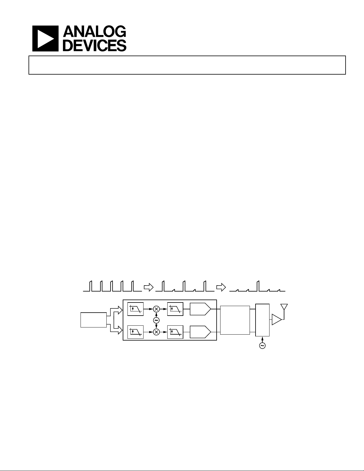
TYPICAL SIGNAL CHAIN
COMPLEX BAS EBAND
DC
2
DIGITAL
BASEBAND
PROCESSOR
NOTES
1. AQM = ANALOG QUADRATURE MODULATOR.
SIN
COS
2
Rev. 0
Information furnished by Analog Devices is believed to be accurate and reliable. However, no
responsibility is assumed by Analog Devices for its use, nor for any infringements of patents or other
rights of third parties that may result from its use. Specifications subject to change without notice. No
license is granted by implication or otherwise under any patent or patent rights of Analog Devices.
Trademarks and registered trademarks are the property of their respective owners.
COMPL E X I F
2/4
2/4
RF
f
IF
I DAC
ANTIALIASING
FILTER
Q DAC
Figure 1.
One Technology Way, P.O. Box 9106, Norwood, MA 02062-9106, U.S.A.
Tel: 781.329.4700 www.analog.com
Fax: 781.461.3113 ©2010 Analog Devices, Inc. All rights reserved.
LO – f
IF
AQM
LO
PA
09016-001

AD9125
TABLE OF CONTENTS
Features .............................................................................................. 1
Applications ....................................................................................... 1
General Description ......................................................................... 1
Product Highlights ........................................................................... 1
Typical Signal Chain ......................................................................... 1
Revision History ............................................................................... 2
Functional Block Diagram .............................................................. 3
Specifications ..................................................................................... 4
DC Specifications ......................................................................... 4
Digital Specifications ................................................................... 5
Latency and Power-Up Timing Specifications ......................... 5
AC Specifications .......................................................................... 6
Absolute Maximum Ratings ............................................................ 7
Thermal Resistance ...................................................................... 7
ESD Caution .................................................................................. 7
Pin Configuration and Function Descriptions ............................. 8
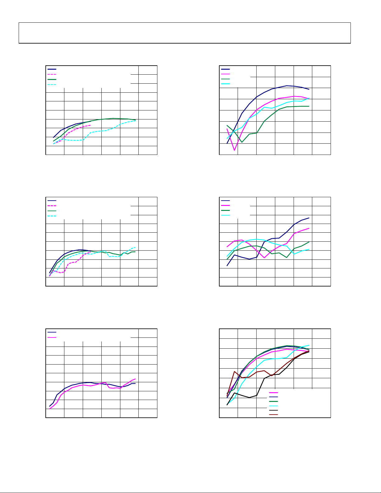
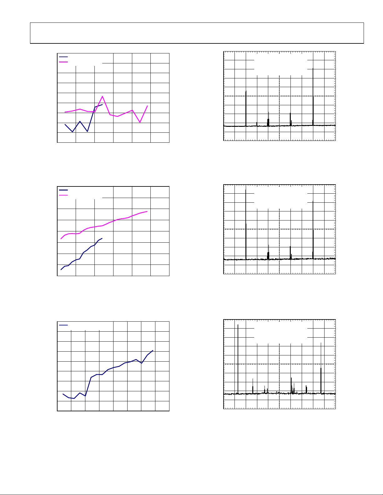
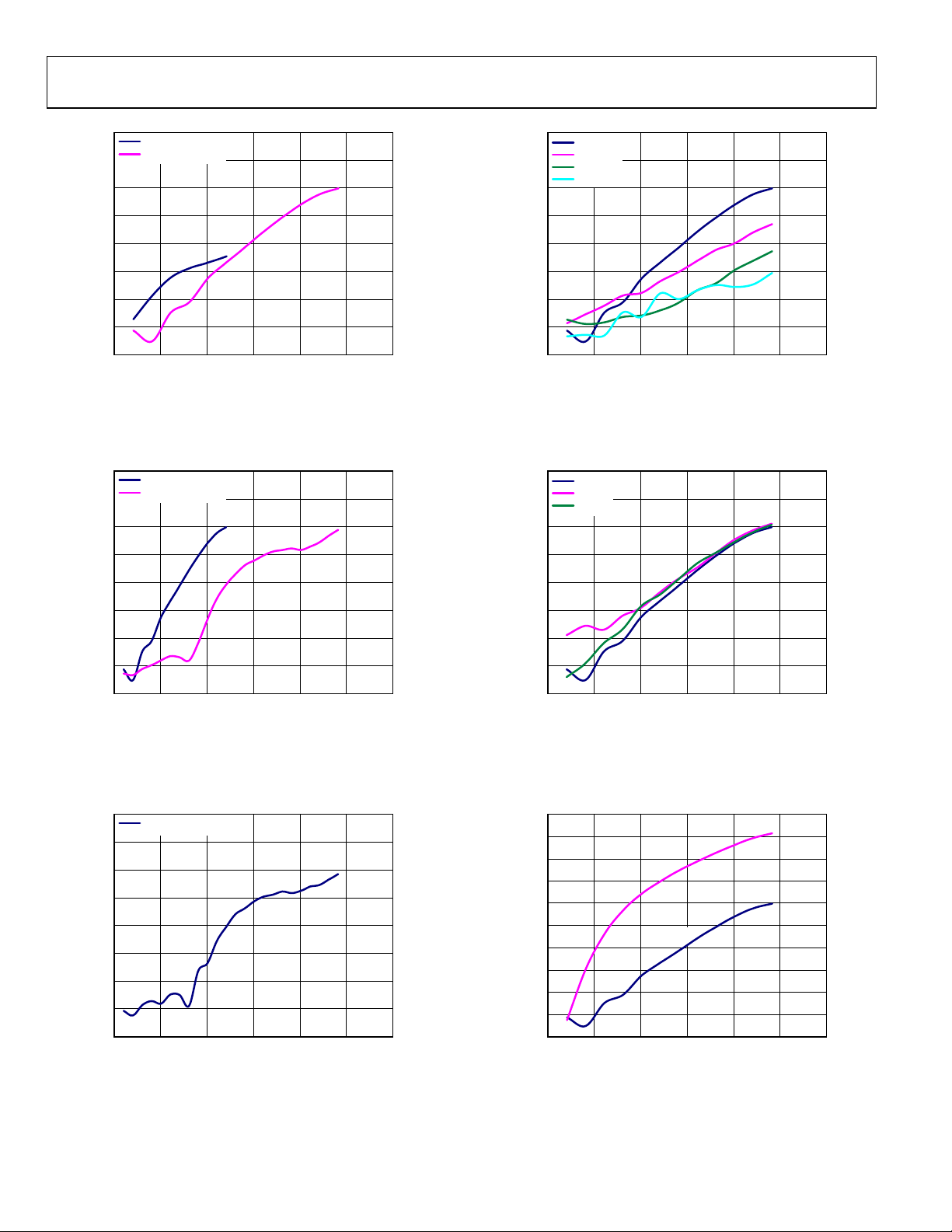
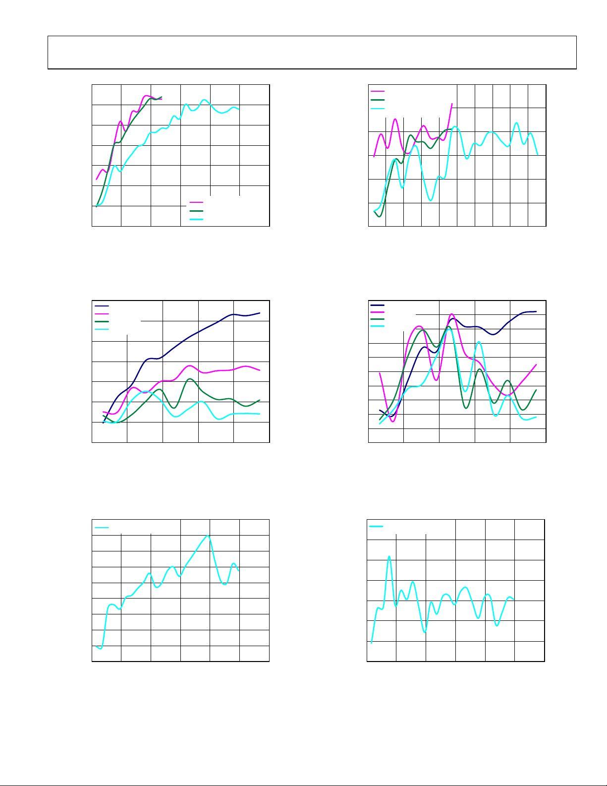
Typical Performance Characteristics ........................................... 10
Terminolog y .................................................................................... 16
Theory of Operation ...................................................................... 17
Serial Port Operation ................................................................. 17
Data Format ................................................................................ 17
Serial Port Pin Descriptions ...................................................... 17
Serial Port Options ..................................................................... 18
Device Configuration Register Map ............................................ 19
Device Configuration Register Descriptions .......................... 21
CMOS Input Data Ports ................................................................ 29
Dual-Word Mode ....................................................................... 29
Word Mode ................................................................................. 29
Byte Mode .................................................................................... 29
Interface Timing ......................................................................... 30
FIFO Operation .......................................................................... 30
Digital Datapath .............................................................................. 32
Premodulation ............................................................................ 32
Interpolation Filters ................................................................... 32
NCO Modulation ....................................................................... 35
Datapath Configuration ............................................................ 35
Determining Interpolation Filter Modes ................................ 36
Datapath Configuration Example ............................................ 37
Data Rates vs. Interpolation Modes ......................................... 38
Coarse Modulation Mixing Sequences .................................... 38
Quadrature Phase Correction ................................................... 39
DC Offset Correction ................................................................ 39
Inverse Sinc Filter ....................................................................... 39
DAC Input Clock Configurations ................................................ 40
DAC Input Clock Configurations ............................................ 40
Analog Outputs............................................................................... 42
Transmit DAC Operation .......................................................... 42
Auxiliary DAC Operation ......................................................... 43
Baseband Filter Implementation .............................................. 44
Driving the ADL5375-15 .......................................................... 44
Reducing LO Leakage and Unwanted Sidebands .................. 44
Device Power Dissipation .............................................................. 45
Temperature Sensor ................................................................... 46
Multichip Synchronization ............................................................ 47
Synchronization with Clock Multiplication ............................... 47
Synchronization with Direct Clocking .................................... 49
Data Rate Mode Synchronization ............................................ 49
FIFO Rate Mode Synchronization ........................................... 50
Additional Synchronization Features ...................................... 51
Interrupt Request Operation ........................................................ 52
Interrupt Service Routine .......................................................... 52
Interface Timing Validation .......................................................... 53
SED Operation ............................................................................ 53
SED Example .............................................................................. 53
Example Start-Up Routine ........................................................ 54
Outline Dimensions ....................................................................... 55
Ordering Guide .......................................................................... 55
REVISION HISTORY
6/10—Revision 0: Initial Version
Rev. 0 | Page 2 of 56
AD9125
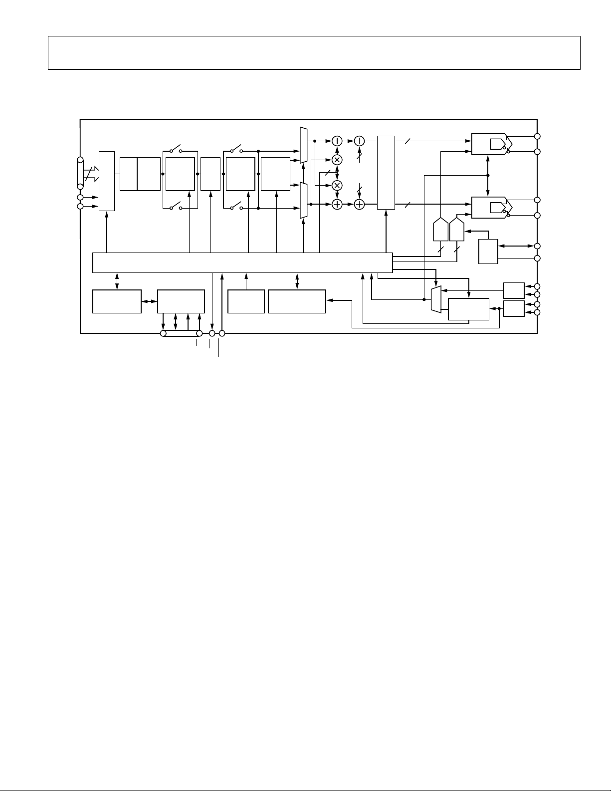
FUNCTIONAL BLOCK DIAGRAM
D[31:0]
DCI
FRAME
f
/2
DATA
PRE
FIFO HB1 HB2 HB3
DATA
RECEIVER
MODE
PROGRAMMING
REGISTERS
MOD
SERIAL
INPUT/OUTPUT
PORT
SDO
NCO
AND
MOD
HB1_CLK
INTERNAL CL OCK TIMING AND CONT ROL LOGIC
CS
SDIO
IRQ
SCLK
10
HB2_CLK
HB3_CLK
INTP
FACTOR
PHASE
CORRECTION
POWER-ON
RESET
RESET
MULTICHIP
SYNCHRONIZATION
SYNC
Figure 2. AD9125 Functional Block Diagram
16
I OFFSET
Q OFFSET
16
16
INV
SINC
16
INVSINC_CLK
PLL CONTROL
DACCLK
PLL_LOCK
GAIN 110GAIN 2
10
DAC CLK_SEL
0
1
MULTIPLIER
(2× TO 16×)
DACCLK
CLOCK
1.2G
DAC 1
16-BIT
1.2G
DAC 1
16-BIT
REF
AND
BIAS
AUX
AUX
CLK
RCVR
CLK
RCVR
IOUT1P
IOUT1N
IOUT2P
IOUT2N
REFIO
FSADJ
DACCLKP
DACCLKN
REFCLKP
REFCLKN
09016-002
Rev. 0 | Page 3 of 56

AD9125
SPECIFICATIONS
DC SPECIFICATIONS
T
to T
MIN
Table 1.
Parameter Min Typ Max Unit
RESOLUTION 16 Bits
ACCURACY
Differential Nonlinearity (DNL) ±2.1 LSB
Integral Nonlinearity (INL) ±3.7 LSB
MAIN DAC OUTPUTS
Offset Error −0.001 0 +0.001 % FSR
Gain Error (with Internal Reference) −3.6 ±2 +3.6 % FSR
Full-Scale Output Current1 8.66 19.6 31.66 mA
Output Compliance Range −1.0 +1.0 V
Output Resistance 10 MΩ
Gain DAC Monotonicity Guaranteed
Settling Time to Within ±0.5 LSB 20 ns
MAIN DAC TEMPERATURE DRIFT
Offset 0.04 ppm/°C
Gain 100 ppm/°C
Reference Voltage 30 ppm/°C
REFERENCE
Internal Reference Voltage 1.2 V
Output Resistance 5 kΩ
ANALOG SUPPLY VOLTAGES
AVDD33 3.13 3.3 3.47 V
CVDD18 1.71 1.8 1.89 V
DIGITAL SUPPLY VOLTAGES
DVDD18 1.71 1.8 1.89 V
IOVDD 1.71 1.8/3.3 3.47 V
POWER CONSUMPTION
2× Mode, f
2× Mode, f
8× Mode, f
AVDD33 55 58 mA
CVDD18 78 85 mA
DVDD18 440 490 mA
Power-Down Mode 1.5 2.7 mW
Power Supply Rejection Ratio, AVDD33 −0.3 +0.3 % FSR/V
OPERATING RANGE −40 +25 +85 °C
1
Based on a 10 kΩ external resistor.
, AVDD33 = 3.3 V, DVDD18 = 1.8 V, CVDD18 = 1.8 V, I
MAX
= 491.52 MSPS, IF = 10 MHz, PLL Off 834 mW
DAC
= 491.52 MSPS, IF = 10 MHz, PLL On 913 mW
DAC
= 800 MSPS, IF = 10 MHz, PLL Off 1114 1227 mW
DAC
= 20 mA, maximum sample rate, unless otherwise noted.
OUTFS
Rev. 0 | Page 4 of 56

AD9125
DIGITAL SPECIFICATIONS
T
to T
MIN
otherwise noted.
Table 2.
Parameter Conditions Min Typ Max Unit
CMOS DATA INPUTS
Input VIN Logic High 1.2 V
Input VIN Logic Low 0.6 V
Maximum Bus Speed 250 MHz
SERIAL PORT OUTPUT LOGIC LEVELS
Output V
IOVDD = 2.5 V 1.8 V
IOVDD = 3.3 V 2.0 V
Output V
IOVDD = 2.5 V 0.4 V
IOVDD = 3.3 V 0.4 V
SERIAL PORT INPUT LOGIC LEVELS
Input VIN Logic High IOVDD = 1.8 V 1.2 V
IOVDD = 2.5 V 1.6 V
IOVDD = 3.3 V 2.4 V
Input VIN Logic Low IOVDD = 1.8 V 0.6 V
IOVDD = 2.5 V 0.8 V
IOVDD = 3.3V 0.8 V
DACCLK INPUT (DACCLKP, DACCLKN)
Differential Peak-to-Peak Voltage 100 500 2000 mV
Common-Mode Voltage Self biased input, ac couple 1.25 V
Maximum Clock Rate 1000 MHz
REFCLK INPUT (REFCLKP, REFCLKN)
Differential Peak-to-Peak Voltage 100 500 2000 mV
Common-Mode Voltage 1.25 V
REFCLKx Frequency, PLL Mode 1 GHz ≤ f
REFCLKx Frequency, SYNC Mode See the Multichip Synchronization section for conditions 0 600 MHz
SERIAL PERIPHERAL INTERFACE
Maximum Clock Rate (SCLK) 40 MHz
Minimum Pulse Width High (t
Minimum Pulse Width Low (t
Setup Time, SDI to SCLK (tDS) 1.9 ns
Hold Time, SDI to SCLK (tDH) 0.2 ns
Data Valid, SDO to SCLK (tDV) 2.3 ns
Setup Time, CS to SCLK (t
, AVDD33 = 3.3 V, IOVDD = 3.3 V, DVDD18 = 1.8 V, CVDD18 = 1.8 V, I
MAX
Logic High IOVDD = 1.8 V 1.4 V
OUT
Logic Low IOVDD = 1.8 V 0.4
OUT
≤ 2.1 GHz 15.625 600 MHz
VCO
) 12.5 ns
PWH
) 12.5 ns
PWOL
) 1.4 ns
D
CS
= 20 mA, maximum sample rate, unless
OUTFS
LATENCY AND POWER-UP TIMING SPECIFICATIONS
Table 3.
Parameter Min Typ Max Unit
LATENCY (DACCLK Cycles)
1× Interpolation (with or Without Modulation) 64 Cycles
2× Interpolation (with or Without Modulation) 135 Cycles
4× Interpolation (with or Without Modulation) 292 Cycles
8× Interpolation (with or Without Modulation) 608 Cycles
Inverse Sinc 20 Cycles
Fine Modulation 8 Cycles
Power-Up Time 260 ms
Rev. 0 | Page 5 of 56

AD9125
AC SPECIFICATIONS
T
to T
MIN
Table 4.
Parameter Min Typ Max Unit
SPURIOUS-FREE DYNAMIC RANGE (SFDR)
f
DAC
f
DAC
f
DAC
f
DAC
TWO-TONE INTERMODULATION DISTORTION (IMD)
f
DAC
f
DAC
f
DAC
f
DAC
NOISE SPECTRAL DENSITY (NSD) EIGHT-TONE, 500 kHz TONE SPACING
f
DAC
f
DAC
f
DAC
W-CDMA ADJACENT CHANNEL LEAKAGE RATIO (ACLR), SINGLE CARRIER
f
DAC
f
DAC
f
DAC
W-CDMA SECOND ACLR, SINGLE CARRIER
f
DAC
f
DAC
f
DAC
, AVDD33 = 3.3 V, DVDD18 = 1.8 V, CVDD18 = 1.8 V, I
MAX
= 100 MSPS, f
= 200 MSPS, f
= 400 MSPS, f
= 800 MSPS, f
= 200 MSPS, f
= 400 MSPS, f
= 400 MSPS, f
= 800 MSPS, f
= 200 MSPS, f
= 400 MSPS, f
= 800 MSPS, f
= 491.52 MSPS, f
= 491.52 MSPS, f
= 983.04 MSPS, f
= 491.52 MSPS, f
= 491.52 MSPS, f
= 983.04 MSPS, f
= 20 MHz 78 dBc
OUT
= 50 MHz 80 dBc
OUT
= 70 MHz 69 dBc
OUT
= 70 MHz 72 dBc
OUT
= 50 MHz 84 dBc
OUT
= 60 MHz 86 dBc
OUT
= 80 MHz 84 dBc
OUT
= 100 MHz 81 dBc
OUT
= 80 MHz −162 dBm/Hz
OUT
= 80 MHz −163 dBm/Hz
OUT
= 80 MHz −164 dBm/Hz
OUT
= 10 MHz 82 dBc
OUT
= 122.88 MHz 80 dBc
OUT
= 122.88 MHz 81 dBc
OUT
= 10 MHz 88 dBc
OUT
= 122.88 MHz 86 dBc
OUT
= 122.88 MHz 88 dBc
OUT
= 20 mA, maximum sample rate, unless otherwise noted.
OUTFS
Table 5. Interface Speeds
Mode Interpolation f
f
BUS
f
DATA
DAC
Byte Mode 1× 250 62.5 62.5
2× (HB1) 250 62.5 125
2× (HB2) 250 62.5 125
4× 250 62.5 250
8× 250 62.5 500
Word Mode 1× 250 125 125
2× (HB1) 250 125 250
2× (HB2) 250 125 250
4× 250 125 500
8× 250 125 1000
Dual-Word Mode 1× 250 250 250
2× (HB1) 250 250 500
2× (HB2) 250 250 500
4× 250 250 1000
8× 125 125 1000
Rev. 0 | Page 6 of 56
AD9125
ABSOLUTE MAXIMUM RATINGS
Table 6.
With
Parameter
AVDD33
IOVDD
DVDD18, CVDD18
AVS S
EPAD
CVSS
DVSS
FSADJ, REFIO,
IOUT1P/IOUT1N,
IOUT2P/IOUT2N
D[31:0], FRAME, DCI EPAD, DVSS −0.3 V to DVDD18 + 0.3 V
DACCLKP/DACCLKN,
REFCLKP/REFCLKN
RESET, IRQ, CS, SCLK,
SDIO, SDO
Junction Temperature 125°C
Storage Temperature
Range
Respect To Rating
AVSS, EPAD,
CVSS, DVSS
AVSS, EPAD,
CVSS, DVSS
AVSS, EPAD,
CVSS, DVSS
EPAD, CVSS,
DVSS
AVSS, CVSS,
DVSS
AVSS, EPAD,
DVSS
AVSS, EPAD,
CVSS
AVSS −0.3 V to AVDD33 + 0.3 V
DVSS −0.3 V to CVDD18 + 0.3 V
EPAD, DVSS −0.3 V to IOVDD + 0.3 V
−65°C to +150°C
−0.3 V to +3.6 V
−0.3 V to +3.6 V
−0.3 V to +2.1 V
−0.3 V to +0.3 V
−0.3 V to +0.3 V
−0.3 V to +0.3 V
−0.3 V to +0.3 V
Stresses above those listed under Absolute Maximum Ratings
may cause permanent damage to the device. This is a stress
rating only; functional operation of the device at these or any
other conditions above those indicated in the operational
section of this specification is not implied. Exposure to absolute
maximum rating conditions for extended periods may affect
device reliability.
THERMAL RESISTANCE
The exposed paddle (EPAD) must be soldered to the ground
plane for the 72-lead LFCSP. The EPAD performs as an
electrical and thermal connection to the board.
Typical θ
, θJB, and θJC values are specified for a 4-layer board in
JA
still air. Airflow increases heat dissipation, effectively reducing
θ
and θJB.
JA
Table 7. Thermal Resistance
Package θJA θJB θJC Unit Conditions
72-Lead LFCSP 20.7 10.9 1.1 °C/W EPAD soldered
ESD CAUTION
Rev. 0 | Page 7 of 56
AD9125
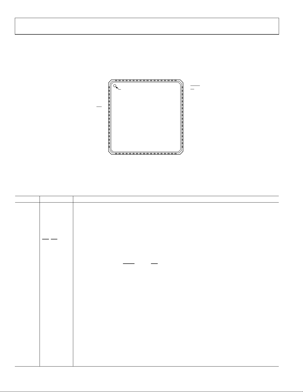
PIN CONFIGURATION AND FUNCTION DESCRIPTIONS
CVDD18
CVDD18
REFCLKP
REFCLKN
AVDD33
IOUT1P
IOUT1N
AVDD33
AVSS
FSADJ
REFIO
AVSS
AVDD33
IOUT2N
IOUT2P
AVDD33
AVSS
NC
7271706968676665646362616059585756
55
CVDD18
DACCLKP
DACCLKN
DVDD18
NOTES
1. NC = NO CONNECT.
2. EXPOSED PAD MUST BE CONNECTED TO AVSS.
CVSS
FRAME
NC
IRQ
D31
D30
NC
IOVDD
D29
D28
D27
D26
1
2
3
4
5
6
7
8
9
10
11
12
13
14
15
16
17D25
18D24
PIN 1
INDICATOR
(Not to S cale)
192021222324252627282930313233
D23
D22
D21
D20
D19
D18
D17
AD9125
TOP VIEW
NC
DCI
D16
DVSS
DVDD18
D15
D14
D13
34
D12
35D11
36D10
54
53
52
51
50
49
48
47
46
45
44
43
42
41
40
39
38
37
RESET
CS
SCLK
SDIO
SDO
DVDD18
D0
D1
D2
D3
DVSS
DVDD18
D4
D5
D6
D7
D8
D9
09016-003
Figure 3. Pin Configuration
Table 8. Pin Function Descriptions
Pin No. Mnemonic Description
1 CVDD18 1.8 V Clock Supply. Supplies clock receivers, clock distribution, and PLL circuitry.
2 DACCLKP DAC Clock Input, Positive.
3 DACCLKN DAC Clock Input, Negative.
4 CVSS Clock Supply Common.
5 FRAME Frame Input.
6 NC No Connect
7
IRQ
(INT)
Interrupt Request. Open Drain, Active Low Output. Connect external pull-up to IOVDD.
8 D31 Data Bit 31.
9 D30 Data Bit 30.
10 NC No Connect.
11 IOVDD
Supply for Serial Port Pin, RESET
Pin, and IRQ Pin. 1.8 V to 3.3 V can be applied to this pin.
12 DVDD18 1.8 V Digital Supply. Supplies power to digital core and digital data ports.
13 D29 Data Bit 29.
14 D28 Data Bit 28.
15 D27 Data Bit 27.
16 D26 Data Bit 26.
17 D25 Data Bit 25.
18 D24 Data Bit 24.
19 D23 Data Bit 23.
20 D22 Data Bit 22.
21 D21 Data Bit 21.
22 D20 Data Bit 20.
23 D19 Data Bit 19.
24 D18 Data Bit 18.
25 D17 Data Bit 17.
26 D16 Data Bit 16.
27 DCI Data Clock Input.
Rev. 0 | Page 8 of 56

AD9125
Pin No. Mnemonic Description
28 NC No Connect.
29 DVDD18 1.8 V Digital Supply.
30 DVSS Digital Common.
31 D15 Data Bit 15.
32 D14 Data Bit 14.
33 D13 Data Bit 13.
34 D12 Data Bit 12.
35 D11 Data Bit 11.
36 D10 Data Bit 10.
37 D9 Data Bit 9.
38 D8 Data Bit 8.
39 D7 Data Bit 7.
40 D6 Data Bit 6.
41 D5 Data Bit 5.
42 D4 Data Bit 4.
43 DVDD18 1.8 V Digital Supply.
44 DVSS Digital Supply Common.
45 D3 Data Bit 3.
46 D2 Data Bit 2.
47 D1 Data Bit 1.
48 D0 Data Bit 0.
49 DVDD18 1.8 V Digital Supply.
50 SDO Serial Port Data Output (CMOS levels with respect to IOVDD).
51 SDIO Serial Port Data Input/Output (CMOS levels with respect to IOVDD).
52 SCLK Serial Port Clock Input (CMOS levels with respect to IOVDD).
53
54
55 NC No Connect.
56 AVSS Analog Supply Common.
57 AVDD33 3.3 V Analog Supply.
58 IOUT2P Q DAC Positive Current Output.
59 IOUT2N Q DAC Negative Current Output.
60 AVDD33 3.3 V Analog Supply.
61 AVSS Analog Supply Common.
62 REFIO Voltage Reference. Nominally 1.2 V output. Should be decoupled to analog common.
63 FSADJ Full-Scale Current Output Adjust. Place a 10 kΩ resistor on the analog common.
64 AVSS Analog Common.
65 AVDD33 3.3 V Analog Supply.
66 IOUT1N I DAC Negative Current Output.
67 IOUT1P I DAC Positive Current Output.
68 AVDD33 3.3 V Analog Supply.
69 REFCLKN PLL Reference Clock Input, Negative. This pin has a secondary function as the SYNC input.
70 REFCLKP PLL Reference Clock Input, Positive. This pin has a secondary function as the SYNC input.
71 CVDD18 1.8 V Clock Supply. Supplies clock receivers, clock distribution, and PLL circuitry.
72 CVDD18 1.8 V Clock Supply. Supplies clock receivers, clock distribution, and PLL circuitry.
EPAD
CS
RESET
Serial Port Chip Select. Active Low (CMOS levels with respect to IOVDD).
Reset. Active Low (CMOS levels with respect to IOVDD).
Exposed pad must be connected to AVSS. This provides an electrical, thermal, and mechanical connection
to the PCB.
Rev. 0 | Page 9 of 56
AD9125
TYPICAL PERFORMANCE CHARACTERISTICS
0
f
= 125MSPS, S E COND HARMONIC
DATA
f
–10
–20
–30
–40
–50
–60
HARMONICS (dBc)
–70
–80
–90
–100
0 50 100 150 200 250 300
Figure 4. Harmonics vs. f
= 125MSPS, THIRD HARMONIC
DATA
f
= 250MSPS, S E COND HARMONIC
DATA
f
= 250MSPS, THIRD HARMONIC
DATA
f
(MHz)
OUT
over f
OUT
Digital Scale = 0 dBFS, f
, 2× Interpolation,
DATA
= 20 mA
SC
09016-101
–50
–55
–60
–65
–70
–75
HARMONICS (dBc)
–80
–85
–90
Figure 7. Second Harmonic vs. f
0dBFS
–6dBFS
–12dBFS
–18dBFS
0 50 100150200250300
f
(MHz)
OUT
over Digital Scale, 2× Interpolation,
OUT
= 250 MSPS, fSC = 20 mA
f
DATA
09016-104
0
f
= 125MSPS, S E COND HARMONIC
DATA
f
–10
–20
–30
–40
–50
–60
HARMONICS (d Bc)
–70
–80
–90
–100
0 100 200 300 400 500 600
Figure 5. Harmonics vs. f
0
–10
–20
–30
–40
–50
–60
HARMONICS (dBc)
–70
–80
–90
–100
0 100 200 300 400 500 600
Figure 6. Harmonics vs. f
= 125MSPS, THIRD HARMONIC
DATA
f
= 250MSPS, S E COND HARMONIC
DATA
f
= 250MSPS, THIRD HARMONIC
DATA
f
(MHz)
OUT
over f
OUT
Digital Scale = 0 dBFS, f
f
= 125MSPS, S E COND HARMONIC
DATA
f
= 125MSPS, THIRD HARMONIC
DATA
f
(MHz)
OUT
over f
OUT
Digital Scale = 0 dBFS, f
, 4× Interpolation,
DATA
= 20 mA
SC
, 8× Interpolation,
DATA
= 20 mA
SC
–50
–55
–60
–65
–70
–75
–80
HARMONICS (d Bc)
–85
–90
–95
–100
09016-102
Figure 8. Third Harmonic vs. f
–50
–55
–60
–65
–70
–75
–80
HARMONICS (dBc)
–85
–90
–95
09016-103
0dBFS
–6dBFS
–12dBFS
–18dBFS
0 50 100150200250300
f
(MHz)
OUT
over Digital Scale, 2× Interpolation,
OUT
= 250 MSPS, fSC = 20 mA
f
DATA
10mA, SECOND HARMONI C
20mA, SECOND HARMONI C
30mA, SECOND HARMONI C
10mA, THIRD HARMONIC
20mA, THIRD HARMONIC
30mA, THIRD HARMONIC
0 50 100150200250300
f
(MHz)
OUT
Figure 9. Harmonics vs. f
= 250 MSPS, Digital Scale = 0 dBFS
f
DATA
over fSC, 2× Interpolation,
OUT
09016-105
09016-106
Rev. 0 | Page 10 of 56
AD9125
–50
–55
–60
–65
–70
–75
–80
–85
HIGHEST DIGITAL S P UR ( dBc)
–90
–95
Figure 10. Highest Digital Spur vs. f
f
= 125MSPS
DATA
f
= 250MSPS
DATA
0 50 100 150 200 250 300
f
(MHz)
OUT
Digital Scale = 0 dBFS, f
OUT
over f
, 2× Interpolation,
DATA
= 20 mA
SC
2× INTERPO LATION,
SINGLE-TONE SPECTRUM,
f
= 250MSPS,
DATA
f
= 101MHz
OUT
START 1.0 MHz
#RES BW 10kHz
09016-107
VBW 10kHz STOP 500.0M Hz
SWEEP 6.017s (601 PTS)
09016-110
Figure 13. 2× Interpolation, Single-Tone Spectrum
–50
–55
–60
–65
–70
–75
–80
HIGHEST DIGITAL S P UR ( dBc)
–85
–90
Figure 11. Highest Digital Spur vs. f
–50
–55
–60
–65
–70
–75
–80
–85
HIGHEST DIGITAL S P UR ( dBc)
–90
–95
Figure 12. Highest Digital Spur vs. f
f
= 125MSPS
DATA
f
= 250MSPS
DATA
0 100 200 300 400 500 600
f
(MHz)
OUT
040035030025020015010050
Digital Scale = 0 dBFS, f
f
= 125MSPS
DATA
Digital Scale = 0 dBFS, f
f
OUT
OUT
(MHz)
OUT
over f
over f
, 4× Interpolation,
DATA
= 20 mA
SC
, 8× Interpolation,
DATA
= 20 mA
SC
4× INTERPO LATION,
SINGLE-TONE SPECTRUM,
f
= 125MSPS,
DATA
f
= 101MHz
OUT
START 1.0 MHz
#RES BW 10kHz
09016-108
VBW 10kHz STOP 500.0M Hz
SWEEP 6.017s (601 PTS)
09016-111
Figure 14. 4× Interpolation, Single-Tone Spectrum
8× INTERPO LATION,
SINGLE-TONE SPECTRUM,
f
= 125MSPS,
DATA
f
= 131MHz
OUT
START 1.0 MHz
#RES BW 10kHz
09016-109
VBW 10kHz STOP 1.0G Hz
SWEEP 12.05s (601 PTS)
09016-112
Figure 15. 8× Interpolation, Single-Tone Spectrum
Rev. 0 | Page 11 of 56
AD9125
–50
–55
–60
f
DATA
f
DATA
= 125MSPS
= 250MSPS
–50
–55
–60
0dBFS
–6dBFS
–12dBFS
–18dBFS
–65
–70
IMD (dBc)
–75
–80
–85
–90
0 50 100 150 200 250 300
f
(MHz)
OUT
–50
–55
–60
–65
–70
IMD (dBc)
–75
–80
–85
Figure 16. IMD vs. f
Digital Scale = 0 dBFS, f
f
= 125MSPS
DATA
f
= 250MSPS
DATA
OUT
over f
, 2× Interpolation,
DATA
= 20 mA
SC
–65
–70
IMD (dBc)
–75
–80
–85
–90
0 50 100 150 200 250 300
f
(MHz)
09016-113
Figure 19. IMD vs. f
f
DATA
–50
–55
–60
–65
–70
IMD (dBc)
–75
–80
–85
20mA
30mA
10mA
OUT
over Digital Scale, 2× Interpolation,
OUT
= 250 MSPS, fSC = 20 mA
09016-116
–90
0 100 200 300 400 500 600
f
(MHz)
OUT
Figure 17. IMD vs. f
Digital Scale = 0 dBFS, f
–50
–55
–60
–65
–70
IMD (dBc)
–75
–80
–85
–90
f
= 125MSPS
DATA
0 100 200 300 400 500 600
Figure 18. IMD vs. f
Digital Scale = 0 dBFS, f
OUT
OUT
over f
f
OUT
over f
, 4× Interpolation,
DATA
= 20 mA
SC
(MHz)
, 8× Interpolation,
DATA
= 20 mA
SC
–90
0 50 100 150 200 250 300
f
(MHz)
09016-114
Figure 20. IMD vs. f
OUT
OUT
over fSC, 2× Interpolation, f
= 250 MSPS,
DATA
09016-117
Digital Scale = 0 dBFS
–40
–45
–50
–55
–60
–65
IMD (dBc)
–70
–75
–80
–85
–90
0 50 100 150 200 250 300
09016-115
PLL ON
PLL OFF
Figure 21. IMD vs. f
f
(MHz)
OUT
, PLL On vs. PLL Off
OUT
09016-118
Rev. 0 | Page 12 of 56
AD9125
–154
–156
–158
–160
–162
NSD (dBm/Hz)
–164
–166
–168
0600500400300200100
Figure 22. One-Tone NSD vs. f
Scale = 0 dBFS, f
2×,
f
DATA
4×,
f
DATA
8×,
f
DATA
f
(MHz)
OUT
over Interpolation Rate and f
OUT
= 20 mA, PLL Off
SC
= 250MSPS
= 125MSPS
= 125MSPS
DATA
09016-119
, Digital
–160
–161
–162
–163
NSD (dBm/Hz)
–164
–165
–166
Figure 25. Eight-Tone NSD vs. f
2×,
f
= 250MSPS
DATA
4×,
f
= 125MSPS
DATA
8×,
f
= 125MSPS
DATA
0 50 100 150 200 250 300 350 400 500450
f
(MHz)
OUT
over Interpolation Rate and f
OUT
Digital Scale = 0 dBFS, f
= 20 mA, PLL Off
SC
DATA
09016-122
,
–154
–156
–158
–160
–162
NSD (dBm/Hz)
–164
–166
–168
0dBFS
–6dBFS
–12dBFS
–18dBFS
025020015010050
Figure 23. One-Tone NSD vs. f
4× Interpolation, f
–158
–159
–160
–161
–162
–163
NSD (dBm/Hz)
–164
–165
–166
–167
8×,
0600500400300200100
f
DATA
= 125MSPS
Figure 24. One-Tone NSD vs. f
Digital Scale = 0 dBFS, f
f
(MHz)
OUT
over Digital Scale, f
OUT
= 20 mA, PLL Off
SC
f
(MHz)
OUT
over Interpolation Rate and f
OUT
= 20 mA, PLL On
SC
DATA
= 200 MSPS,
,
DATA
–161.5
–162.0
–162.5
–163.0
–163.5
–164.0
–164.5
NSD (dBm/Hz)
–165.0
–165.5
–166.0
–166.5
09016-120
Figure 26. Eight-Tone NSD vs. f
–160
–161
–162
–163
–164
NSD (dBm/Hz)
–165
–166
–167
09016-121
Figure 27. Eight-Tone NSD vs. f
0dBFS
–6dBFS
–12dBFS
–18dBFS
0 50 100 150 200 250
f
(MHz)
OUT
over Digital Scale, f
OUT
4× Interpolation, f
8×,
f
= 125MSPS
DATA
0 100 200 300 500400 600
Digital Scale = 0 dBFS, f
= 20 mA, PLL Off
SC
f
(MHz)
OUT
over Interpolation Rate and f
OUT
= 20 mA, PLL On
SC
= 200 MSPS,
DATA
DATA
09016-123
09016-124
,
Rev. 0 | Page 13 of 56
AD9125
ACLR (dBc)
–77
–78
–79
–80
–81
–82
–83
0dBFS
–3dBFS
–6dBFS
ACLR (dBc)
–50
–55
–60
–65
–70
–75
–80
–85
2×, PLL OFF
4×, PLL OFF
2×, PLL ON
4×, PLL ON
–84
0 50 100 150 200 250
f
(MHz)
OUT
Figure 28. One-Carrier W-CDMA ACLR vs. f
over Digital Cutback,
OUT
Adjacent Channel, PLL Off
–78
–80
–82
–84
ACLR (dBc)
–86
–88
–90
0dBFS
–3dBFS
–6dBFS
0 50 100 150 200 250
f
(MHz)
OUT
Figure 29. One-Carrier W-CDMA ACLR vs. f
OUT
Alternate Channel, PLL Off
–70
–75
0dBFS
–3dBFS
–6dBFS
over f
DAC
–90
0 100 200 300 400 500
f
(MHz)
09016-125
Figure 31. One-Carrier W-CDMA ACLR vs. f
OUT
over Interpolation Rate,
OUT
09016-128
Adjacent Channel, PLL On vs. PLL Off
–70
–72
–74
–76
–78
–80
–82
ACLR (dBc)
–84
–86
–88
–90
09016-126
,
Figure 32. One-Carrier W-CDMA ACLR vs. f
2×, PLL OFF
4×, PLL OFF
2×, PLL ON
4×, PLL ON
0 100 200 300 400 500
f
(MHz)
OUT
over Interpolation Rate,
OUT
09016-129
Alternate Channel, PLL On vs. PLL Off
–70
–75
2×, PLL OFF
4×, PLL OFF
2×, PLL ON
4×, PLL ON
–80
–85
ACLR (dBc)
–90
–95
0 50 100 150 200 250
f
(MHz)
OUT
Figure 30. One-Carrier W-CDMA ACLR vs. f
OUT
Second Alternate Channel, PLL Off
over f
DAC
09016-127
,
Rev. 0 | Page 14 of 56
–80
ACLR (dBc)
–85
–90
–95
0 100 200 300 400 500
f
(MHz)
OUT
Figure 33. One-Carrier W-CDMA ACLR vs. f
over Interpolation Rate,
OUT
Second Alternate Channel, PLL On vs. PLL Off
09016-130
AD9125
START 133.06M Hz
#RES BW 30kHz
RMS RESULTS FREQ LOWER UPPER
CARRIER POWER 5.00MHz 3.840MHz –75.96 –85.96 –77.13 –87.13
–10.00dBm/ 10.00MHz 3.840MHz –85.33 –95.33 –85.24 –95.25
3.840MHz 15.00MHz 2.888MHz –95.81 –95.81 –85.43 –95.43
OFFSET REF BW dBc dBm dBc dBm
VBW 30kHz STOP 166.94MHz
SWEEP 143.6ms (601 PTS)
Figure 34. Four-Carrier W-CDMA ACLR Performance, IF ≈150 MHz
START 125.88MHz
#RES BW 30kHz
TOTAL CARRIER POWER: –11.19dBm/15.3600MHz
RRC FILTER: OFF FILTER ALPHA 0.22
REF CARRIER POWER: –16.89dBm/3.84000MHz
09016-131
1 –16.92dBm 5.000MHz 3.840MHz –65.88 –82.76 –67.52 –84.40
2 –16.89dBm 10.00MHz 3.840MHz –68.17 –85.05 –69.91 –86.79
3 –17.43dBm 15.00MHz 3.840MHz –70.42 –87.31 –71.40 –88.28
4 –17.64dBm
OFFSET FREQ INTEG BW dBc dBm dBc dBm
VBW 30kHz S TOP 174.42M Hz
SWEEP 206.9ms (601 PTS)
LOWER UPPER
09016-132
Figure 35. One-Carrier W-CDMA ACLR Performance, IF ≈150 MHz
Rev. 0 | Page 15 of 56
AD9125
TERMINOLOGY
Integral Nonlinearity (INL)
INL is defined as the maximum deviation of the actual analog
output from the ideal output, determined by a straight line drawn
from zero scale to full scale.
Differential Nonlinearity (DNL)
DNL is the measure of the variation in analog value, normalized
to full scale, associated with a 1 LSB change in digital input code.
Offset Error
The deviation of the output current from the ideal of zero is
called offset error. For IOUT1P, 0 mA output is expected when
the inputs are all 0s. For IOUT1N, 0 mA output is expected
when all inputs are set to 1.
Gain Error
The difference between the actual and ideal output span. The
actual span is determined by the difference between the outputs
when all inputs are set to 1 vs. when all inputs are set to 0.
Output Compliance Range
The range of allowable voltage at the output of a current output
DAC. Operation beyond the maximum compliance limits can
cause either output stage saturation or breakdown, resulting in
nonlinear performance.
Temp er at u re D ri ft
Temperature drift is specified as the maximum change from
the ambient (25°C) value to the value at either T
MIN
or T
MAX
.
For offset and gain drift, the drift is reported in ppm of fullscale range (FSR) per degree Celsius. For reference drift, the
drift is reported in ppm per degree Celsius.
Power Supply Rejection (PSR)
The maximum change in the full-scale output as the supplies
are varied from minimum to maximum specified voltages.
Settling Time
The time required for the output to reach and remain within a
specified error band around its final value, measured from
the start of the output transition.
Spurious-Free Dynamic Range (SFDR)
The difference in decibels between the peak amplitude of the
output signal and the peak spurious signal within the dc to the
Nyquist frequency of the DAC. Typically, energy in this band is
rejected by the interpolation filters. This specification, therefore,
defines how well the interpolation filters work and the effect of
other parasitic coupling paths to the DAC output.
Signal-to-Noise Ratio (SNR)
SNR is the ratio of the rms value of the measured output signal
to the rms sum of all other spectral components below the Nyquist
frequency, excluding the first six harmonics and dc. The value
for SNR is expressed in decibels.
Interpolation Filter
If the digital inputs to the DAC are sampled at a multiple rate of
f
(interpolation rate), a digital filter can be constructed that
DATA
has a sharp transition band near f
appear around f
(output data rate) can be greatly suppressed.
DAC
/2. Images that typically
DATA
Adjacent Channel Leakage Ratio (ACLR)
The ratio in decibels relative to the carrier (dBc) between the
measured power within a channel and that of its adjacent channel.
Complex Image Rejection
In a traditional two-part upconversion, two images are created
around the second IF frequency. These images have the effect
of wasting transmitter power and system bandwidth. By placing
the real part of a second complex modulator in series with the
first complex modulator, either the upper or lower frequency
image near the second IF can be rejected.
DATA
DCI
LATCH
INPUT
f
INTERFACE
DATA
FORMAT
32
WRITE
POINTER
16
2
FIFO
16
2
READ
POINTER
f
/
f
DATA
HB1
Figure 36. Defining Data Rates
Rev. 0 | Page 16 of 56
f
SIN
NCO
COS
CLOCK GENERATOR
AND DISTRIBUTOR
/
f
NCO
HB2
16
22
22
f
HB3
I DAC
16
Q DAC
DACCLK
f
DAC
09016-136

AD9125
THEORY OF OPERATION
The AD9125 combines many features that make it a very attractive
DAC for wired and wireless communications systems. The dual
digital signal path and dual DAC structure allow an easy interface
to common quadrature modulators when designing single
sideband transmitters. The speed and performance of the AD9125
allows wider bandwidths and more carriers to be synthesized than
in previously available DACs. In addition, these devices include an
innovative low power, 32-bit, complex NCO that greatly increases
the ease of frequency placement.
The AD9125 offers features that allow simplified synchronization
with incoming data and between multiple devices. Auxiliary
DACs are also provided on chip for output dc offset compensation
(for local oscillator [LO] compensation in single sideband [SSB]
transmitters) and for gain matching (for image rejection
optimization in SSB transmitters).
SERIAL PORT OPERATION
The serial port is a flexible, synchronous serial communication
port, allowing easy interface to many industry-standard microcontrollers and microprocessors. The serial I/O is compatible
with most synchronous transfer formats, including both the
Motorola SPI® and Intel® SSR protocols. The interface allows
read/write access to all registers that configure the AD9125.
Single- or multiple-byte transfers are supported, as well as MSBfirst or LSB-first transfer formats. The serial interface ports can
be configured as a single-pin I/O (SDIO) or two unidirectional
pins for input/output (SDIO/SDO).
50
SDO
51
SDIO
SCLK
Figure 37. Serial Port Interface Pins
There are two phases of a communication cycle with the
AD9125. Phase 1 is the instruction cycle (the writing of an
instruction byte into the device), which is coincident with the
first eight SCLK rising edges. The instruction byte provides the
serial port controller with information regarding the data
transfer cycle, which is Phase 2 of the communication cycle.
The Phase 1 instruction byte defines whether the upcoming
data transfer is a read or write and the starting register address
for the first byte of the data transfer. The first eight SCLK rising
edges of each communication cycle are used to write the
instruction byte into the device.
A logic high on the
CS
pin followed by a logic low resets the
serial port timing to the initial state of the instruction cycle.
From this state, the next eight rising SCLK edges represent the
instruction bits of the current I/O operation.
CS
SPI
PORT
52
53
09016-010
The remaining SCLK edges are for Phase 2 of the communication
cycle. Phase 2 is the actual data transfer between the device and
the system controller. Phase 2 of the communication cycle is a
transfer of one or more data bytes. Registers change immediately
upon writing to the last bit of each transfer byte, except for the
frequency tuning word and NCO phase offsets, which only change
when the frequency update bit (Register 0x36, Bit 0) is set.
DATA FORMAT
The instruction byte contains the information shown in Tab l e 9 .
Table 9. Serial Port Instruction Byte
I7 (MSB) I6 I5 I4 I3 I2 I1 I0 (LSB)
R/W
A6 A5 A4 A3 A2 A1 A0
R/W, Bit 7 of the instruction byte, determines whether a read or
write data transfer occurs after the instruction byte write. Logic 1
indicates a read operation, and Logic 0 indicates a write
operation.
A6 to A0, Bit 6 to Bit 0 of the instruction byte, determine the
register that is accessed during the data transfer portion of the
communication cycle. For multibyte transfers, A6 is the starting
byte address. The remaining register addresses are generated by
the device based on the LSB_FIRST bit (Register 0x00, Bit 6).
SERIAL PORT PIN DESCRIPTIONS
Serial Clock (SCLK)
The serial clock pin synchronizes data to and from the device
and runs the internal state machines. The maximum frequency
of SCLK is 40 MHz. All data input is registered on the rising
edge of SCLK. All data is driven out on the falling edge of SCLK.
Chip Select (
An active low input starts and gates a communication cycle.
It allows more than one device to be used on the same serial
communication lines. The SDO and SDIO pins go to a high
impedance state when this input is high. During the
communication cycle, the
Serial Data I/O (SDIO)
Data is always written into the device on this pin. However, this
pin can be used as a bidirectional data line. The configuration
of this pin is controlled by Register 0x00, Bit 7. The default is
Logic 0, configuring the SDIO pin as unidirectional.
Serial Data Out (SDO)
Data is read from this pin for protocols that use separate lines
for transmitting and receiving data. In the case where the device
operates in a single bidirectional I/O mode, this pin does not
output data and is set to a high impedance state.
CS
)
CS
pin should stay low.
Rev. 0 | Page 17 of 56

AD9125
SERIAL PORT OPTIONS
The serial port can support both MSB-first and LSB-first data
formats. This functionality is controlled by the LSB_FIRST bit
(Register 0x00, Bit 6). The default is MSB-first (LSB_FIRST = 0).
When LSB_FIRST = 0 (MSB-first), the instruction and data bit
must be written from MSB to LSB. Multibyte data transfers in
MSB-first format start with an instruction byte that includes the
register address of the most significant data byte. Subsequent data
bytes should follow from the high address to the low address. In
MSB-first mode, the serial port internal byte address generator
decrements for each data byte of the multibyte communication cycle.
When LSB_FIRST = 1 (LSB-first), the instruction and data bit
must be written from LSB to MSB. Multibyte data transfers in
LSB-first format start with an instruction byte that includes the
register address of the least significant data byte followed by
multiple data bytes. The serial port internal byte address generator
increments for each byte of the multibyte communication cycle.
The serial port controller data address decrements from the
data address written toward 0x00 for multibyte I/O operations
if the MSB-first mode is active. The serial port controller address
increments from the data address written toward 0x7F for
multibyte I/O operations if the LSB-first mode is active.
INSTRUCTION CYCLE DATA TRANSFER CYCLE
CS
SCLK
SDIO
SDO
R/W A6 A5 A4 A3 A2 A1 A0 D7 D6ND5
D7 D6ND5
Figure 38. Serial Register Interface Timing, MSB First
INSTRUCTION CYCLE DATA TRANSFER CYCLE
CS
SCLK
SDIO
SDO
A0 A1 A2 A3 A4 N0 N1 R/W D00D10D2
D00D10D2
Figure 39. Serial Register Interface Timing, LSB First
t
CS
SCLK
SDIO
DS
t
DS
t
PWH
t
t
SCLK
t
PWL
DH
INSTRUCTION BIT 6INSTRUCTION BIT 7
Figure 40. Timing Diagram for Serial Port Register Write (t
CS
N
N
0
0
D00D10D20D3
0
D00D10D20D3
0
N
N
to t
DS
09016-011
D7ND6ND5ND4
D7ND6ND5ND4
09016-012
09016-013
)
CS
D
SCLK
t
DV
SDIO,
SDO
DATA BIT n – 1DATA BIT n
09016-014
Figure 41. Timing Diagram for Serial Port Register Read
Rev. 0 | Page 18 of 56

AD9125
DEVICE CONFIGURATION REGISTER MAP
Table 10. Device Configuration Register Map
Register Name
Comm 0x00 SDIO LSB_FIRST Reset 0x00
Power Control 0x01 Power-
Data Format 0x03 Binary
Interrupt Enable 1 0x04 Enable
Interrupt Enable 2 0x05 0 0 0 Enable
Event Flag 1 0x06 PLL
Event Flag 2 0x07 AED
Clock Receiver
Control
PLL Control 1 0x0A PLL
PLL Control 2 0x0C PLL loop bandwidth[2:0] PLL charge pump current[4:0] 0xD1
PLL Control 3 0x0D N2[1:0] PLL cross
PLL Status 1 0x0E PLL lock VCO control voltage[3:0] 0x00
PLL Status 2 0x0F VCO band readback[5:0] 0x00
Sync Control 1 0x10 Sync
Sync Control 2 0x11 Sync phase request[5:0] 0x00
Sync Status 1 0x12 Sync lost Sync
Sync Status 2 0x13 Sync phase readback[7:0] (6.2 format) N/A
FIFO Control 0x17 FIFO phase offset[2:0] 0x04
FIFO Status 1 0x18 FIFO
FIFO Status 2 0x19 FIFO level[7:0] N/A
Datapath Control 0x1B Bypass
HB1 Control 0x1C HB1[1:0] Bypass HB1 0x00
HB2 Control 0x1D HB2[5:0] Bypass HB2 0x00
HB3 Control 0x1E HB3[5:0] Bypass HB3 0x00
Chip ID 0x1F Chip ID[7:0] 0x08
Addr
(Hex)
0x08 DACCLK
Bit 7 Bit 6 Bit 5 Bit 4 Bit 3 Bit 2 Bit 1 Bit 0 Default
down
DAC I
data
format
PLL lock
lost
lock
lost
duty
correction
enable
enable
Warning 1
premod
Powerdown
DAC Q
Q data
first
Enable
PLL
lock
PLL
locked
REFCLK
duty
correction
PLL
manual
enable
Data/FIFO
rate toggle
locked
FIFO
Warning 2
Bypass
−1
sinc
Powerdown data
receiver
MSB swap Data bus width[1:0] 0x00
Enable
sync
signal
lost
Sync
signal
lost
DACCLK
cross-
correction
Rising
N/A
FIFO soft
Bypass
NCO
Powerdown
aux ADC
Enable
sync
signal
lock
AED
compare
pass
Sync
signal
locked
compare
pass
REFCLK
cross-
correction
control
enable
NCO gain Bypass
PLL lock
Enable
sync
phase
lock
Enable
AED
compare
fail
Sync
phase
locked
AED
compare
fail
1 1 1 1 0x3F
Manual VCO band[5:0] 0x40
edge sync
Enable
soft
FIFO
sync
Enable
SED
compare
fail
Soft
FIFO
sync
SED
compare
fail
N0[1:0] N1[1:0] 0xD9
align ack
phase
compensation and
dc offset
Enable
FIFO
Warning 1
0 0 0x00
FIFO
Warning 1
N/A
Sync Averaging[2:0] 0x48
FIFO soft
align
request
Select
sideband
status
Enable
FIFO
Warning 2
FIFO
Warning 2
FIFO reset
aligned
Send I data
to Q data
0x10
0x00
N/A
N/A
0xE4
Rev. 0 | Page 19 of 56

AD9125
Register Name
FTW 1 (LSB) 0x30 FTW[7:0] 0x00
FTW 2 0x31 FTW[15:8] 0x00
FTW 3 0x32 FTW[23:16] 0x00
FTW 4 (MSB) 0x33 FTW[31:24] 0x00
NCO Phase Offset
LSB
NCO Phase Offset
MSB
NCO FTW Update 0x36 Frame
I Phase Adj LSB 0x38 I phase adjust[7:0] 0x00
I Phase Adj MSB 0x39 I phase adjust[9:8] 0x00
Q Phase Adj LSB 0x3A Q phase adjust[7:0] 0x00
Q Phase Adj MSB 0x3B Q phase adjust[9:8] 0x00
I DAC Offset LSB 0x3C I DAC offset[7:0] 0x00
I DAC Offset MSB 0x3D I DAC offset[15:8] 0x00
Q DAC Offset LSB 0x3E Q DAC offset[7:0] 0x00
Q DAC Offset MSB 0x3F Q DAC offset[15:8] 0x00
I DAC FS Adjust 0x40 I DAC FS adjust[7:0] 0xF9
I DAC Control 0x41 I DAC
Aux DAC I Data 0x42 I aux DAC[7:0] 0x00
I Aux DAC
Control
Q DAC FS Adjust 0x44 Q DAC FS adjust[7:0] 0xF9
Q DAC Control 0x45 Q DAC
Aux DAC Q Data 0x46 Q aux DAC[7:0] 0x00
Q Aux DAC
Control
Die Temperature
Range Control
Die Temperature
LSB
Die Temperature
MSB
SED Control 0x67 SED
Compare I0 LSBs 0x68 Compare Value I0[7:0] 0xB6
Compare
I0 MSBs
Compare
Q0 LSBs
Compare
Q0 MSBs
Compare I1 LSBs 0x6C Compare Value I1[7:0] 0x16
Compare I1 MSBs 0x6D Compare Value I1[15:8] 0x1A
Compare
Q1 LSBs
Addr
(Hex) Bit 7 Bit 6 Bit 5 Bit 4 Bit 3 Bit 2 Bit 1 Bit 0 Default
0x34 NCO phase offset[7:0] 0x00
0x35 NCO phase offset[15:8] 0x00
FTW ack
sleep
0x43 I Aux
DAC sign
sleep
0x47 Q Aux
DAC sign
0x48 FS current[2:0] Reference current[2:0] Capacitor
0x49 Die temperature[7:0] N/A
0x4A Die temperature[15:8] N/A
compare
enable
0x69 Compare Value I0[15:8] 0x7A
0x6A Compare Value Q0[7:0] 0x45
0x6B Compare Value Q0[15:8] 0xEA
0x6E Compare Value Q1[7:0] 0xC6
I DAC FS adjust[9:8] 0x01
I Aux DAC
current
direction
Q DAC FS adjust[9:8] 0x01
Q Aux DAC
current
direction
Sample
I aux DAC
sleep
Q aux
DAC
sleep
error
detected
Frame FTW
request
I aux DAC[9:8] 0x00
Q aux DAC[9:8] 0x00
Auto-
Update
Compare
clear
enable
FTW ack
fail
Update
FTW
request
value
Compare
pass
0x00
0x02
0x00
Rev. 0 | Page 20 of 56

AD9125
Register Name
Compare
Q1 MSBs
SED I LSBs 0x70 Errors detected I_BITS[7:0] 0x00
SED I MSBs 0x71 Errors detected I_BITS[15:8] 0x00
SED Q LSBs 0x72 Errors detected Q_BITS[7:0] 0x00
SED Q MSBs 0x73 Errors detected Q_BITS[15:8] 0x00
Die Revsion 0x7F Revision[3:0] 0x0C
DEVICE CONFIGURATION REGISTER DESCRIPTIONS
Table 11. Device Configuration Register Descriptions
Register
Name
Comm 0x00 7 SDIO SDIO operation. 0
0 = SDIO operates as an input only.
1 = SDIO operates as a bidirectional input/output.
6 LSB_FIRST Serial port communication LSB or MSB first. 0
0 = MSB first.
1 = LSB first.
5 Reset
Power Control 0x01 7 Power-down DAC I 1 = powers down DAC I. 0
6 Power-down DAC Q 1 = powers down DAC Q. 0
5
4
0 PLL lock status 1 = PLL is locked. 0
Data Format 0x03 7 Binary data format 0 = input data is in twos complement format. 0
1 = input data is in binary format.
6 Q data first Indicates I/Q data pairing on data input. 0
0 = I data sent to data receiver first.
1 = Q data sent to data receiver first.
5 MSB swap Swaps the bit order of the data input port. 0
[1:0] Data bus width Data receiver interface mode. 0
00 = dual-word mode; 32-bit interface bus width.
01 = word mode; 16-bit interleaved interface bus width.
10 = byte mode; 8-bit interleaved interface bus width.
11 = invalid.
Interrupt Enable 1 0x04 7 Enable PLL lock lost 1 = enables interrupt for PLL lock lost. 0
6 Enable PLL lock 1 = enables interrupt for PLL lock. 0
5 Enable sync signal lost 1 = enables interrupt for sync signal lock lost. 0
4 Enable sync signal lock 1 = enables interrupt for sync signal lock. 0
3
2 Enable soft FIFO sync 1 = enables interrupt for soft FIFO reset. 0
Addr
(Hex) Bit 7 Bit 6 Bit 5 Bit 4 Bit 3 Bit 2 Bit 1 Bit 0 Default
0x6F Compare Value Q1[15:8] 0xAA
Address
(Hex) Bits Name Description Default
0
0
Power-down data
receiver
Power-down auxiliary
ADC
Enable sync phase
locked
1 = device is held in reset when this bit is written high
and is held there until the bit is written low.
1 = powers down the input data receiver. 0
1 = powers down the auxiliary ADC for temperature
sensor.
0 = order of the data bits corresponds to the pin
descriptions.
1 = bit designations are swapped; most significant bits
become the least significant bits.
See the CMOS Input Data Ports section for details on
the operation of the different interface modes.
1 = enables interrupt for clock generation ready. 0
Rev. 0 | Page 21 of 56

AD9125
Register
Name
1 Enable FIFO Warning 1 1 = enables interrupt for FIFO Warning 1. 0
0 Enable FIFO Warning 2 1 = enables interrupt for FIFO Warning 2. 0
Interrupt Enable 2 0x05 7 Set to 0 Set this bit to 0. 0
Event Flag 11 0x06 7 PLL lock lost
6 PLL locked
5 Sync signal lost
4 Sync signal locked
3 Sync phase locked
2 Soft FIFO sync
1 FIFO Warning 1
0 FIFO Warning 2
Event Flag 21 0x07 4 AED comparison pass
3 AED comparison fail
2 SED comparison fail
Clock Receiver
Control
4 REFCLK cross-correction
Address
(Hex) Bits Name Description Default
6 Set to 0 Set this bit to 0. 0
5 Set to 0 Set this bit to 0. 0
4
3
2
1 Set to 0 Set this bit to 0. 0
0 Set to 0 Set this bit to 0. 0
0x08 7 DACCLK duty correction 1 = enables duty-cycle correction on the DACCLK input. 0
6 REFCLK duty correction 1 = enables duty-cycle correction on the REFCLK input. 0
5 DACCLK cross-correction
Enable AED comparison
pass
Enable AED comparison
fail
Enable SED comparison
fail
1 = enables interrupt for AED comparison pass. 0
1 = enables interrupt for AED comparison fail. 0
1 = enables interrupt for SED comparison fail. 0
1 = indicates that the PLL, which had been previously
locked, has unlocked from the reference signal. This is a
latched signal.
1 = indicates that the PLL has locked to the reference
clock input.
1 = indicates that the sync logic, which had been
previously locked, has lost alignment. This is a latched
signal.
1 = indicates that the sync logic did achieve sync
alignment. This is indicated when no phase changes
were requested for at least a few full averaging cycles.
1 = indicates that the internal digital clock generation logic
is ready. This occurs when internal clocks are present and
stable.
1 = indicates that a FIFO reset originating from a serial
port-based request has successfully completed. This is a
latched signal.
1 = indicates that the difference between the FIFO read
and write pointers is 1.
1 = indicates that the difference between the FIFO read
and write pointers is 2.
1 = indicates that the SED logic detected a valid input
data pattern compared with the preprogrammed
expected values. This is a latched signal.
1 = indicates that the SED logic detected an invalid
input data pattern compared with the preprogrammed
expected values. This is a latched signal that automatically clears when eight valid I/Q data pairs are
received.
1 = indicates that the SED logic detected an invalid
input data pattern compared with the preprogrammed
expected values. This is a latched signal.
1 = enables differential crossing correction on the DACCLK
input.
1 = enables differential crossing correction on the
REFCLK input.
0
0
0
0
0
0
0
0
0
0
1
1
Rev. 0 | Page 22 of 56

AD9125
Register
Name
PLL Control 1 0x0A 7 PLL enable
6 PLL manual enable Enables the manual selection of the VCO band. 1
[5:0] Manual VCO band Selects the VCO band to be used. 0
PLL Control 2 0x0C [7:5]
PLL Control 3 0x0D [7:6] N2[1:0]
00 = f
01 = f
10 = f
11 = f
4 PLL cross control enable Enables PLL cross-point controller. 1
[3:2] N0[1:0]
00 = f
01 = f
10 = f
11 = f
[1:0] N1[1:0]
00 = f
01 = f
10 = f
11 = f
PLL Status 1 0x0E 7 PLL lock
PLL Status 2 0x0F [5:0]
Sync Control 1 0x10 7 Sync enable 1 = enables the synchronization logic. 0
6 Data/FIFO rate toggle 0 = operates the synchronization at the FIFO reset rate. 1
1 = operates the synchronization at the data rate.
3 Rising edge sync 0 = sync is initiated on the falling edge of the sync input. 1
1 = sync is initiated on the rising edge of the sync input.
[2:0] Sync averaging[2:0]
000 = 1.
001 = 2.
010 = 4.
011 = 8.
100 = 16.
101 = 32.
Address
(Hex) Bits Name Description Default
1 = enables the PLL clock multiplier. REFCLK input is
0
used as the PLL reference clock signal.
1 = manual mode; the correct VCO band must be
determined by the user.
PLL loop
000 = loop bandwidth is nominally 200 kHz
bandwidth[2:0]
Selects the PLL loop filter bandwidth. 110
010 = loop bandwidth is nominally 450 kHz
100 = loop bandwidth is nominally 950 kHz
110 = loop bandwidth is nominally 2 MHz
[4:0]
00000 = lowest current setting.
PLL charge pump
current[4:0]
Sets the nominal PLL charge-pump current. 10001
11111 = highest current setting.
PLL control clock divider. These bits determine the ratio
3
of the DACCLK rate to the PLL controller clock rate.
must always be less than 80 MHz.
f
PC_CLK
DACCLK/fPC_CLK
DACCLK/fPC_CLK
DACCLK/fPC_CLK
DACCLK/fPC_CLK
PLL VCO divider. These bits determine the ratio of the
= 2.
= 4.
= 8.
= 16.
10
VCO output to the DACCLK frequencies.
VCO/fDACCLK
VCO/fDACCLK
VCO/fDACCLK
VCO/fDACCLK
PLL loop divider. These bits determine the ratio of the
= 1.
= 2.
= 4.
= 4.
01
DACCLK to the REFCLK frequencies.
DACCLK/fREFCLK
DACCLK/fREFCLK
DACCLK/fREFCLK
DACCLK/fREFCLK
The PLL generated clock is tracking the REFCLK input
= 2.
= 4.
= 8.
= 16.
R
signal.
[3:0]
VCO control
VCO control voltage readback (see Table 25). R
voltage[3:0]
VCO band
Indicates the VCO band currently selected. R
readback[5:0]
Sets the number of input samples that are averaged for
0
determining the sync phase.
Rev. 0 | Page 23 of 56

AD9125
Register
Name
110 = 64.
111 = 128.
Sync Control 2 0x11 5:0 Sync phase request[5:0]
000000 = 0 DACCLK cycles.
000001 = 1 DACCLK cycle.
…
111111 = 63 DACCLK cycles.
Sync Status 1 0x12 7 Sync lost
Sync Status 2 0x13 [7:0] Sync phase readback[7:0]
00000000 = 0.0.
00000001 = 0.25.
…
11111110 = 63.50.
11111111 = 63.75.
FIFO Control 0x17 [2:0] FIFO phase offset[2:0]
000 = 0.
001 = 1.
…
111 = 7.
FIFO Status 1 0x18 7 FIFO Warning 1 FIFO read and write pointers within ±1. 0
6 FIFO Warning 2 FIFO read and write pointers within ±2. 0
2
1 FIFO soft align request
0 FIFO reset aligned
FIFO Status 2 0x19 [7:0] FIFO level[7:0] Thermometer encoded measure of the FIFO level. 0
Datapath Control 0x1B 7 Bypass premod 1 = bypasses fS/2 premodulator. 1
6 Bypass sinc−1 1 = bypasses inverse sinc filter. 1
5 Bypass NCO 1 = bypasses NCO. 1
3 NCO gain
2
Address
(Hex) Bits Name Description Default
This sets the requested clock phase offset after sync.
The offset unit is in DACCLK cycles. This enables
repositioning of the DAC output with respect to the
sync input. The offset can also be used to skew the DAC
outputs between the synchronized DACs.
1 = indicates that synchronization had been attained
but was subsequently lost.
6 Sync locked 1 = indicates that synchronization has been attained. R
Indicates the averaged sync phase offset (6.2 format). If
the value differs from the requested sync phase value,
this indicates sync timing errors.
FIFO write pointer phase offset following FIFO reset.
This is the difference between the read pointer and the
write pointer values upon FIFO reset. The optimal value
is nominally 4.
FIFO soft align
acknowledge
Bypass phase compensation and dc offset
FIFO read and write pointers are aligned after a serial
port initiated FIFO reset.
Request FIFO read and write pointers alignment via the
serial port.
FIFO read and write pointers aligned after a hardware
reset.
0 = default. No gain scaling is applied to the NCO input
to the internal digital modulator.
1 = gain scaling of 0.5 is applied to the NCO input to the
internal digital modulator. This can eliminate saturation
of the modulator output for some combinations of data
inputs and NCO signals.
1 = bypasses phase compensation and dc offset. 1
0
R
R
4
0
0
0
Rev. 0 | Page 24 of 56

AD9125
Register
Name
1 Select sideband 0 = the modulator outputs high-side image. 0
0 Send I data to Q data
HB1 Control 0x1C [2:1] HB1[1:0]
HB2 Control 0x1D [6:1] HB2[5:0] Modulation mode for I Side Half-Band Filter 2. 0
HB3 Control 0x1E [6:1] HB3[5:0] Modulation mode for I Side Half-Band Filter 3. 0
0 Bypass HB3 1 = bypasses third-stage interpolation filter. 0
Chip ID 0x1F [7:0] Chip ID[7:0] This register identifies the device as an AD9125. 8
Address
(Hex) Bits Name Description Default
1 = the modulator outputs low-side image. The image is
spectrally inverted compared with the input data.
1 = ignores Q data from the interface and disables the
0
clocks to the Q datapath. Sends I data to both the I and
Q DACs.
0
00 = input signal is not modulated; filter pass band is
from −0.4 to +0.4 of f
.
IN1
01 = input signal is not modulated; filter pass band is
from 0.1 to 0.9 of f
10 = input signal is modulated by f
from 0.6 to 1.4 of f
11 = input signal is modulated by f
from 1.1 to 1.9 of f
.
IN1
; filter pass band is
.
IN1
.
IN1
IN1
; filter pass band is
IN1
0 Bypass HB1 1 = bypasses first-stage interpolation filter. 0
000000 = input signal is not modulated; filter pass band
is from −0.25 to +0.25 of f
.
IN2
001001 = input signal is not modulated; filter pass band
is from 0.0 to 0.5 of f
.
IN2
010010 = input signal is not modulated; filter pass band
is from 0.25 to 0.75 of f
.
IN2
011011 = input signal is not modulated; filter pass band
is from 0.5 to 1.0 of f
100100 = input signal is modulated by f
band is from 0.75 to 1.25 of f
101101 = input signal is modulated by f
band is from 1.0 to 1.5 of f
110110 = input signal is modulated by f
band is from 1.25 to 1.75 of f
111111 = input signal is modulated by f
band is from 1.5 to 2.0 of f
.
IN2
; filter pass
.
IN2
.
IN2
.
IN2
.
IN2
IN2
; filter pass
IN2
; filter pass
IN2
; filter pass
IN2
0 Bypass HB2 1 = bypasses second stage interpolation filter. 0
000000 = input signal is not modulated; filter pass band
is from −0.2 to +0.2 of f
.
IN3
001001 = input signal is not modulated; filter pass band
is from 0.05 to 0.45 of f
.
IN3
010010 = input signal is not modulated; filter pass band
is from 0.3 to 0.7 of f
.
IN3
011011 = input signal is not modulated; filter pass band
is from 0.55 to 0.95 of f
100100 = input signal is modulated by f
band is from 0.8 to 1.2 of f
101101 = input signal is modulated by f
band is from 1.05 to 1.45 of f
110110 = input signal is modulated by f
band is from 1.3 to 1.7 of f
111111 = input signal is modulated by f
band is from 1.55 to 1.95 of f
.
IN3
; filter pass
.
IN3
.
IN3
.
IN3
.
IN3
IN3
; filter pass
IN3
; filter pass
IN3
; filter pass
IN3
Rev. 0 | Page 25 of 56

AD9125
Register
Name
FTW 1 (LSB) 0x30 [7:0] FTW[7:0]
FTW 2 0x31 [7:0] FTW[15:8] See Register 0x30. 0
FTW 3 0x32 [7:0] FTW[23:16] See Register 0x30. 0
FTW 4 (MSB) 0x33 [7:0] FTW[31:24] See Register 0x30. 0
NCO Phase Offset
LSB
NCO Phase Offset
MSB
NCO FTW Update 0x36 5
I Phase Adj LSB 0x38 [7:0] I phase adjust[7:0]
I Phase Adj MSB 0x39 [1:0] I phase adjust[9:8] Register 0x38. 0
Q Phase Adj LSB 0x3A [7:0] Q phase adjust[7:0]
Q Phase Adj MSB 0x3B [1:0] Q phase adjust[9:8] See Register 0x3A. 0
I DAC Offset LSB 0x3C [7:0] I DAC offset[7:0]
I DAC Offset MSB 0x3D [7:0] I DAC offset[15:8] See Register 0x3C. 0
Q DAC Offset LSB 0x3E [7:0] Q DAC offset[7:0]
Q DAC Offset MSB 0x3F [7:0] Q DAC offset[15:8] See Register 0x3E. 0
I DAC FS Adjust 0x40 [7:0] I DAC FS adjust[7:0]
0x000 = 8.64 mA.
…
0x200 = 20.14 mA.
…
0x3FF = 31.66 mA.
I DAC Control 0x41 7 I DAC sleep
Aux DAC I Data 0x42 [7:0] I aux DAC[7:0]
0x000 = 0.000 mA.
0x001 = 0.002 mA.
…
0x3FF = 2.046 mA.
Address
(Hex) Bits Name Description Default
FTW[31:0] is the 32-bit frequency tuning word that
determines the frequency of the complex carrier
generated by the on-chip NCO. The frequency is not
updated when the FTW registers are written. The values
are only updated when Bit 0 of Register 0x36 transitions
from 0 to 1.
0x34 [7:0] NCO phase offset[7:0]
0x35 [7:0] NCO phase offset[15:8] See Register 0x34. 0
FRAME FTW
acknowledge
4 FRAME FTW request
1
0 Update FTW request
[1:0] I DAC FS adjust[9:8] See Register 0x40. 1
Update FTW
acknowledge
Rev. 0 | Page 26 of 56
NCO phase offset[15:0] sets the phase of the complex
carrier signal when the NCO is reset. The phase offset
spans between 0° and 360°. Each bit represents an offset of
0.0055°. The value is in twos complement format.
1 = indicates that the NCO has been reset due to an
extended FRAME pulse signal.
0 → 1 = the NCO is reset on the first extended FRAME
pulse after this bit transitions from 0 to 1.
1 = indicates that the FTW has been updated. 0
0 → 1 = the FTW is updated on 0-to-1 transition of this bit.
I phase adjust[9:0] is used to insert a phase offset
between the I and Q datapaths. This can be used to
correct for phase imbalance in a quadrature modulator.
See the Quadrature Phase Correction section for details.
Q phase adjust[9:0] is used to insert a phase offset
between the I and Q datapaths. This can be used to
correct for phase imbalance in a quadrature modulator.
See the Quadrature Phase Correction section for details.
I DAC offset[15:0] is a value added directly to the
samples written to the I DAC.
Q DAC offset[15:0] is a value added directly to the
samples written to the Q DAC.
I DAC FS adjust[9:0] sets the full-scale current of the
I DAC. The full-scale current can be adjusted from 8.64 mA
to 31.6 mA in step sizes of approximately 22.5 μA.
1 = puts the I-channel DAC into sleep mode (fast wakeup mode).
I aux DAC[9:0] sets the magnitude of the auxiliary DAC
current. The range is 0 mA to 2 mA, and the step size is 2 μA.
0
0
0
0
0
0
0
0
0
F9
0
0

AD9125
Register
Name
I Aux DAC Control 0x43 7 I aux DAC sign
Q DAC FS Adjust 0x44 [7:0] Q DAC FS adjust[7:0]
0x000 = 8.64 mA.
…
0x200 = 20.14 mA.
…
0x3FF = 31.66 mA.
Q DAC Control 0x45 7 Q DAC sleep
Aux DAC Q Data 0x46 [7:0]
0x000 = 0.000 mA.
0x001 = 0.002 mA.
…
0x3FF = 2.046 mA.
Q Aux DAC Control 0x47 7 Q aux DAC sign
6
1 = the auxiliary DAC Q sinks current.
5 Q aux DAC sleep Q-channel auxiliary DAC sleep 0
[1:0] Q aux DAC[9:8] See Register 0x46. 0
Die Temp Range
Control
…
111 = highest current.
[3:1] Reference current[2:0] Auxiliary ADC reference current. 1
000 = lowest current.
111 = highest current.
0 Capacitor value Auxiliary ADC internal capacitor value. 0
0 = 5 pF.
1 = 10 pF.
Die Temp LSB 0x49 [7:0] Die temp[7:0]
0xC422 = 25.1°C.
…
Die Temp MSB 0x4A [7:0] Die temp[15:8] See Register 0x49. R
Address
(Hex) Bits Name Description Default
0 = the auxiliary DAC I sign is positive, and the current is
directed to the IOUT1P pin (Pin 67).
6
1 = the auxiliary DAC I sinks current.
5 I aux DAC sleep I channel auxiliary DAC sleep. 0
[1:0] I Aux DAC[9:8] See Register 0x42. 0
[1:0] Q DAC FS adjust[9:8] See Register 0x44. 1
0x48 [6:4] FS current[2:0] Auxiliary ADC full-scale current. 0
000 = lowest current.
0xADCC = −39.9°C.
I aux DAC current
direction
Q aux DAC[7:0]
Q aux DAC current
direction
1 = the auxiliary DAC I sign is negative, and the current
is directed to the IOUT1N pin (Pin 66).
0 = the auxiliary DAC I sources current. 0
Q DAC FS adjust[9:0] sets the full-scale current of the
I DAC. The full-scale current can be adjusted from 8.64 mA
to 31.6 mA in step sizes of approximately 22.5 μA.
1 = puts the Q-channel DAC into sleep mode (fast wakeup mode).
Q aux DAC[9:0] sets the magnitude of the aux DAC current.
The range is 0 mA to 2 mA, and the step size is 2 μA.
0 = the auxiliary DAC Q sign is positive, and the current
is directed to the IOUT2P pin (Pin 58).
1 = the auxiliary DAC Q sign is negative, and the current
is directed to the IOUT2N pin (Pin 59).
0 = the auxiliary DAC Q sources current. 0
Die Temp[15:0] indicates the approximate die
temperature.
0xD8A8 = 84.8°C (see the Temperature Sensor section for
details).
0
F9
0
0
0
R
Rev. 0 | Page 27 of 56

AD9125
Register
Name
SED Control 0x67 7 SED compare enable
Compare I0 LSBs 0x68 [7:0] Compare Value I0[7:0]
Compare I0 MSBs 0x69 [7:0] Compare Value I0[15:8] See Register 0x68. 7A
Compare Q0 LSBs 0x6A [7:0] Compare Value Q0[7:0]
Compare Q0 MSBs 0x6B [7:0]
Compare I1 LSBs 0x6C [7:0] Compare Value I1[7:0]
Compare I1 MSBs 0x6D [7:0] Compare Value I1[15:8] See Register 0x6C. 1A
Compare Q1 LSBs 0x6E [7:0] Compare Value Q1[7:0]
Compare Q1 MSBs 0x6F [7:0]
SED I LSBs 0x70 [7:0]
SED I MSBs 0x71 [7:0]
SED Q LSBs 0x72 [7:0]
SED Q MSBs 0x73 [7:0]
Die Revision 0x7F [5:2] Revision[3:0] Corresponds to device die revision. 3
1
All bit event flags are cleared by writing the respective bit high.
Address
(Hex) Bits Name Description Default
1 = enables the SED circuitry. None of the flags in this
0
register or the values in Register 0x70 through
Register 0x73 are significant if the SED is not enabled.
5 Sample error detected
1 = indicates an error is detected. The bit remains set
0
until cleared. Any write to this register clears this bit to 0.
3 Autoclear enable
1 = enables autoclear mode. This activates Bit 1 and Bit
0
0 of this register and causes Register 0x70 through
Register 0x73 to be autocleared whenever eight
consecutive error-free sample data sets are received.
1 Compare fail
1 = indicates an error has been detected. This bit
0
remains high until it is autocleared by the reception of
eight consecutive error-free comparisons or until it is
cleared by writing to this register.
0 Compare pass 1 = indicates that the last sample comparison was error free. 0
Compare Value I0[15:0] is the word that is compared
B6
with the I0 input sample captured at the input interface.
Compare Value Q0[15:0] is the word that is compared
45
with the Q0 input sample captured at the input interface.
Compare Value
See Register 0x6A EA
Q0[15:8]
Compare Value I1[15:0] is the word that is compared
16
with the I1 input sample captured at the input interface.
Compare Value Q1[15:0] is the word that is compared
C6
with the Q1 input sample captured at the input interface.
Compare Value
See Register 0x6E. AA
Q1[15:8]
Errors Detected
I_BITS[7:0]
Errors detected
Errors detected I_BITS[15:0] indicates which bits were
received in error.
See Register 0x70. 0
0
I_BITS[15:8]
Errors detected
Q_BITS[7:0]
Errors detected
Errors detected Q_BITS[15:0] indicates which bits were
received in error.
See Register 0x72. 0
0
Q_BITS[15:8]
Rev. 0 | Page 28 of 56

AD9125
CMOS INPUT DATA PORTS
The AD9125 input data port consists of a data clock (DCI),
data bus, and FRAME signal. The data port can be configured
to operate in three modes: dual-word mode, word mode, and
byte mode.
In dual-word mode, I and Q data is received simultaneously on
two 16-pin buses. One bus receives I datapath input words, and
the other bus receives Q datapath input words. In word mode,
one 16-pin bus is used to receive interleaved I and Q input
words. In byte mode, an 8-pin bus is used to receive interleaved
I and Q input bytes. The pin assignments of the bus in each
mode is described in Ta ble 1 2.
Table 12. Data Bit Pin Assignments for Data Input Modes
Mode Data Bus Pin Assignments
Dual Word I data: D[31:16]
Q data: D[15:0]
Word
I and Q data: D[29:28], D[25:24], D[21:20], D[17:16],
D[15:14], D[11:10], D[7:6], D[3:2]
Byte I and Q data: D[21:20], D[17:16], D[15:14], D[11:10]
In byte and word modes, a FRAME signal is required for
controlling which DAC receives the data. In dual-word mode,
the FRAME signal is not required because each DAC has a
dedicated bus.
DUAL-WORD MODE
In dual-word mode, the DCI signal is supplied as a qualifying
clock that is time aligned with the input data. The rising edge of
the DCI signal should be aligned with the changing data of each
of the I and Q input data streams.
DCI
WORD MODE
In word mode, the DCI signal is supplied as a qualifying clock
that is time aligned with the input data. The rising edge of the
DCI signal should be aligned with the changing data of the
interleaved I and Q input data stream. The FRAME signal
indicates to which DAC the data is sent. When FRAME is high,
data is sent to the I DAC. When FRAME is low, data is sent to
the Q DAC. For 14- and 12-bit resolution devices, the two and
four LSBs are not significant, respectively. The complete timing
diagram is shown in Figure 43.
DCI
I AND
Q DATA
FRAME
Figure 43. Timing Diagram for Word Mode
I
1
Q
1
I
2
09016-143
BYTE MODE
In byte mode, the DCI signal is supplied as a qualifying clock
that is time aligned with the input data. The rising edge of the
DCI signal should be aligned with the changing data of the
interleaved I and Q input data stream. The FRAME signal
indicates to which DAC the data is sent. When FRAME is high,
data is sent to the I DAC. When FRAME is low, data is sent to
the Q DAC. Both bytes must be written to each datapath for
proper operation. For 14- and 12-bit resolution devices, the
LSBs in the second byte are not significant. The complete
timing diagram is shown in Figure 44.
DCI
I DATA
Q DATA
Figure 42. Timing Diagram for Dual-Word Mode
I
1
Q
1
I
2
Q
2
I
3
Q
3
09016-142
Rev. 0 | Page 29 of 56
I AND
Q
LSBI1MSBI1LSBQ1MSBQ1LSBI2MSBI2LSBQ2MSBQ2LSB
Q DATA
FRAME
Figure 44. Timing Diagram for Byte Mode
09016-144

AD9125
INTERFACE TIMING
The timing diagram for the digital interface port is shown in
Figure 45. The sampling point of the data bus occurs on the
falling edge of the DCI signal and has an uncertainty of 2.1 ns,
as illustrated by the sampling interval shown in Figure 45. The
D[31:0] and FRAME signals must be valid throughout this
sampling interval.
The setup (t
are shown in Figure 45. The minimum setup and hold times
are shown in Ta bl e 1 3 .
DCI
D[31:0]
FRAME
Table 13. Data Port Setup and Hold Times
Minimum Setup Time, tS (ns) Minimum Hold Time, tH (ns)
0.86 1.24
DCI
FRAME
Table 14. FRAME Setup and Hold Times
Minimum Setup Time, t
(ns)
−0.04 +1.05
) and hold (tH) times with respect to the edges
S
tSt
H
Figure 45. Timing Diagram for Input Data Ports
t
S-FRAME
t
H-FRAME
Figure 46. Timing Diagram for Frame input
S-FRAME
Minimum Hold Time, t
(ns)
H_FRAME
09016-146
09016-147
The data interface timing can be verified by using the sample
error detection (SED) circuitry. See the Interface Timing
Va l id a t i on section for details.
FIFO OPERATION
The AD9125 contains a 2-channel, 16-bit wide, eight-word-deep
FIFO designed to relax the timing relationship between the data
arriving at the DAC input ports and the internal DAC data rate
clock. The FIFO acts as a buffer that absorbs timing variations
between the data source and DAC, such as the clock-to-data
variation of an FPGA or ASIC, which significantly increases the
timing budget of the interface.
Figure 47 shows the block diagram of the datapath through the
FIFO. The data is latched into the device and is formatted, and
then it is written into the FIFO register determined by the FIFO
write pointer. The value of the write pointer is incremented every
time a new word is loaded into the FIFO. Meanwhile, data is
read from the FIFO register determined by the read pointer and
fed into the digital datapath. The value of the read pointer is
updated every time data is read into the datapath from the FIFO.
This happens at the data rate, that is, the DACCLK rate divided by
the interpolation ratio.
Valid data is transmitted through the FIFO as long as the
FIFO does not overflow or become empty. Note that an overflow or empty condition of the FIFO is the same as the write
pointer and read pointer being equal. When both pointers are
equal, an attempt is made to read and write a single FIFO register
simultaneously. This simultaneous register access leads to
unreliable data transfer through the FIFO and must be avoided.
Nominally, data is written to the FIFO at the same rate that data is
read from the FIFO, which keeps the data level in the FIFO constant.
If data is written to the FIFO faster than data is read, the data level
in the FIFO increases. If data is written to the device slower than
data is read, the data level in the FIFO decreases. For an optimum
timing margin, the FIFO level should be maintained near half
full, which is the same as maintaining a difference of four between
the write pointer and read pointer values.
32 BITS
REG 0
REG 1
DATA
INPUT
LATCH
DATA
ASSEMBLER
WRITE POINTER
Figure 47. Block Diagram of Datapath Through FIFO
REG 2
REG 3
REG 4
REG 5
REG 6
REG 7
32 BITS
Rev. 0 | Page 30 of 56
PATHS
READ POINTER
DATA
1616
DACS
÷ INTDCI
DACCLK
09016-018

AD9125
Initializing the FIFO Data Level
To avoid a concurrent read and write to the same FIFO address
and to ensure a fixed pipeline delay, it is important to initialize
the FIFO pointers to known states. The FIFO pointers can be
initialized in two ways: via a write sequence to the serial port or
by strobing the FRAME input. There are two types of FIFO pointer
resets: a relative reset and an absolute reset. A relative reset enforces
a defined FIFO depth. An absolute reset enforces a particular
write pointer value when the reset is initiated. A serial port
initiated FIFO reset is always a relative reset. A FRAME strobe
initiated reset can be either a relative or an absolute reset.
The operation of the FRAME initiated FIFO reset depends on
the synchronization mode chosen. When synchronization is
disabled or when the device is configured for data rate mode
synchronization, the FRAME strobe initiates a relative FIFO
reset. When FIFO mode synchronization is chosen, the FRAME
strobe initiates an absolute FIFO reset. More details on the
synchronization function can be found in the Multichip
Synchronization section.
A summary of the synchronization modes and the type of FIFO
reset employed is listed in Tabl e 15 .
Table 15. Summary of FIFO Resets
FIFO
Reset Signal
Disabled Data Rate FIFO Rate
Synchronization Mode
Serial Port Relative reset Relative reset Relative reset
FRAME Relative reset Relative reset Absolute reset
FIFO Level Initialization via Serial Port
A serial port initiated FIFO reset can be issued in any mode
and always results in a relative FIFO reset. To initialize the FIFO
data level through the serial port, Bit 1 of Register 0x18 should
be toggled from 0 to 1 and then back to 0. When the write to the
register is complete, the FIFO data level is initialized. When the
initialization is triggered, the next time the read pointer becomes
0, the write pointer is set to the value of the FIFO phase offset level
(Register 0x17, Bits[2:0]) variable upon initialization. By default,
this is 4, but it can be programmed to a value between 0 and 7.
The recommended procedure for a serial port FIFO data level
initialization is as follows:
1. Request FIFO level reset by setting Register 0x18, Bit 1, to 1.
2. Verify that the part acknowledges the request by ensuring
that Register 0x18, Bit 2, is 1.
3. Remove the request by setting Register 0x18, Bit 1, to 0.
4. Verify that the part drops the acknowledge signal by
ensuring that Register 0x18, Bit 2, is 0.
FIFO Level Initialization via FRAME Signal
The primary function of the FRAME input is indicating to which
DAC the input data is written. Another function of the FRAME
input is initializing the FIFO data level value. This is done by
asserting the FRAME signal high for at least the time interval
needed to load complete data to the I and Q DACs. This
Rev. 0 | Page 31 of 56
corresponds to one DCI period in dual-word mode, two DCI
periods in word mode, and four DCI periods in byte mode.
To initiate a relative FIFO reset with the FRAME signal, the device
must be configured in data rate mode (Register 0x10, Bit 6). When
FRAME is asserted in data rate mode, the write pointer is set to 4
(by default or to the FIFO start level) the next time the read pointer
becomes 0 (see Figure 48).
READ
POINTER
FRAME
WRITE
POINTER
0 1 2 3 4 5 6 7 0 1 2 3
FIFO WRITE RESETS
3 4 5 6 7 0 1 2 4 5 6 7
Figure 48. FRAME Input vs. Write Pointer Value, Data Rate Mode
Write Pointer Initialization via FRAME Signal
In FIFO rate synchronization mode, the REFCLK/SYNC signal
is used to reset the FIFO read pointer to 0. The edge of the
DAC clock used to sample the SYNC signal is selected by Bit 3
of Register 0x10. The FRAME signal is used to reset the FIFO
write pointer. In the FIFO rate synchronization mode, the FIFO
write pointer is reset immediately after the FRAME signal is
asserted high for at least the time interval needed to load complete
data to the I and Q DACs. The FIFO write pointer is initialized to
the value of the FIFO phase offset[2:0] (Register 0x17). FIFO rate
synchronization is selected by setting Bit 6 of Register 0x10 to 0.
SYNC
FIFO READ RESET
READ
POINTER
FRAME
WRITE
POINTER
01 3210765432
FIFO WRITE
RESET
Figure 49. FRAME Input vs. Write Pointer Value, FIFO Rate Mode
FIFO PHASE OFFSET[2:0]
REGISTER 0x17, BITS[2:0] = 0b101
321076566547
Monitoring the FIFO Status
The FIFO initialization and status can be read from Register 0x18.
This register provides information on the FIFO initialization
method and whether the initialization was successful. The MSB
of Register 0x18 is a FIFO warning flag that can optionally
trigger a device interrupt (
IRQ
). This flag is an indication that
the FIFO is close to emptying (FIFO level is 1) or overflowing
(FIFO level is 7). This is an indication that data may soon be
corrupted and action should be taken.
The FIFO data level can be read from Register 0x19 at any time.
The FIFO data level reported by the serial port is denoted as a
7-bit thermometer code of the write counter state relative to the
absolute read counter being at 0. The optimum FIFO data level of 4
is, therefore, reported as a value of 00001111 in the status register. It
should be noted that, depending on the timing relationship between
DCI and the main DACCLK, the FIFO level value can be off by
±1 count. Therefore, it is important to keep the difference between
the read and write pointers to at least 2.
09016-019
09016-148
AD9125
DIGITAL DATAPATH
The block diagram in Figure 50 shows the functionality of the
digital datapath. The digital processing includes a premodulation
block, three half-band interpolation filters, a quadrature modulator
with a fine resolution NCO, a phase and offset adjustment
block, and an inverse sinc filter.
PREMOD
HB1 HB2 HB3
Figure 50. Block Diagram of Digital Datapath
AND
OFFSET
ADJUST
SINC
–1
09016-020
PHASE
The digital datapath accepts I and Q data streams and processes
them as a quadrature data stream. The signal processing blocks can
be used when the input data stream is represented as complex data.
The datapath can be used to process an input data stream
representing two independent real data streams as well, but
the functionality is somewhat restricted. The premodulation
block can be used, as well as any of the nonshifted interpolation
filter modes (see the Premodulation section for more details).
PREMODULATION
The half-band interpolation filters have selectable pass bands
that allow the center frequencies to be moved in increments of
½ of their input data rate. The premodulation block provides a
digital upconversion of the incoming waveform by ½ of the
incoming data rate, f
. This can be used to frequency-shift
DATA
baseband input data to the center of the interpolation filters’
pass band.
INTERPOLATION FILTERS
The transmit path contains three interpolation filters. Each of
the three interpolation filters provides a 2× increase in output data
rate. The half-band (HB) filters can be individually bypassed or
cascaded to provide 1×, 2×, 4×, or 8× interpolation ratios. Each
of the half-band filter stages offers a different combination of
bandwidths and operating modes.
The bandwidth of the three half-band filters with respect to the
data rate at the filter input is as follows:
• Bandwidth of HB1 = 0.8 × f
• Bandwidth of HB2 = 0.5 × f
• Bandwidth of HB3 = 0.4 × f
IN1
IN2
IN3
Half-Band Filter 1 (HB1)
HB1 has four modes of operation, as shown in Figure 51. The
shape of the filter response is identical in each of the four modes.
The four modes are distinguished by two factors: the filter center
frequency and whether the input signal is modulated by the filter.
MODE 0
0
–20
–40
GAIN (dB)
–60
–80
–100
021.81.61.41.21.00.80.60.40.2
MODE 1 MODE 3
NORMALIZE D FREQUENCY (×
Figure 51. HB1 Filter Modes
MODE 2
.0
f
)
IN1
09016-021
As shown in Figure 51, the center frequency in each mode is
offset by ½ the input data rate (f
) of the filter. Mode 0 and
IN1
Mode 1 do not modulate the input signal. Mode 2 and Mode 3
modulate the input signal by f
. When HB1 operates in Mode 0
IN1
and Mode 2, the I and Q paths operate independently and no
mixing of the data between channels occurs. When HB1 operates
in Mode 1 and Mode 3, mixing of the data between the I and Q
paths occurs; therefore, the data input into the filter is assumed
complex. Tab l e 16 summarizes the HB1 modes.
Table 16. HB1 Filter Mode Summary
Mode f
f
CENTER
Input Data
MOD
0 DC None Real or complex
1 fIN/2 None Complex
2 f
3 3f
f
IN
/2 fIN Complex
IN
Real or complex
IN
The usable bandwidth is defined as the frequency over which
the filters have a pass-band ripple of less than ±0.001 dB and an
image rejection of greater than +85 dB. As is discussed in the
Half-Band Filter 1 (HB1) section, the image rejection usually sets
the usable bandwidth of the filter, not the pass-band flatness.
The half-band filters operate in several modes, providing
programmable pass-band center frequencies as well as signal
modulation. The HB1 filter has four modes of operation, and
the HB2 and HB3 filters each have eight modes of operation.
Rev. 0 | Page 32 of 56

AD9125
Figure 52 shows the pass-band filter response for HB1. In most
applications, the usable bandwidth of the filter is limited by the
image suppression provided by the stop-band rejection, not by
the pass-band flatness. Tabl e 17 shows the pass-band flatness
and stop-band rejection that the HB1 filter supports at different
bandwidths.
0.02
0
–0.02
–0.04
GAIN (dB)
–0.06
Half-Band Filter 2 (HB2)
HB2 has eight modes of operation, as shown in Figure 53 and
Figure 54. The shape of the filter response is identical in each of
the eight modes. The eight modes are distinguished by two factors:
the filter center frequency and whether the input signal is
modulated by the filter.
MODE 0
0
–20
–40
GAIN (dB)
–60
MODE 2 MODE 6
MODE 4
–0.08
–0.10
000.360.320.280.240.200.160.120.080.04
NORMALIZED FREQUENCY (×
f
IN1
40
.
)
09016-022
Figure 52. Pass-Band Detail of HB1
Table 17. HB1 Pass-Band Flatness and Stop-Band Rejection
Bandwidth (% of f
IN1
)
Pass-Band
Flatness (dB)
Stop-Band
Rejection (dB)
80 0.001 85
80.4 0.0012 80
81.2 0.0033 70
82.0 0.0076 60
83.6 0.0271 50
85.6 0.1096 40
–80
–100
021.81.61.41.21.00.80.60.40.2
NORMALIZE D FREQUENCY (×
f
)
IN2
.0
09016-023
Figure 53. HB2, Even Filter Modes
MODE 5
MODE 7
f
IN2
.0
)
09016-024
GAIN (dB)
–20
–40
–60
–80
–100
0
021.81.61.41.21.00.80.60.40.2
MODE 1
NORMALIZE D FREQUENCY (×
MODE 3
Figure 54. HB2, Odd Filter Modes
As shown in Figure 53 and Figure 54, the center frequency in
each mode is offset by ¼ of the input data rate (f
) of the filter.
IN2
Mode 0 through Mode 3 do not modulate the input signal.
Mode 4 through Mode 7 modulate the input signal by f
IN2
.
When HB2 operates in Mode 0 and Mode 4, the I and Q paths
operate independently and no mixing of the data between
channels occurs. When HB2 operates in the other six modes,
mixing of the data between the I and Q paths occurs; therefore,
the data input to the filter is assumed complex.
Rev. 0 | Page 33 of 56
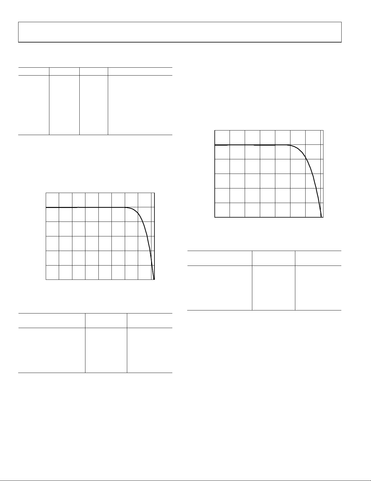
AD9125
Tabl e 18 summarizes the HB2 and HB3 modes.
Table 18. HB2 and HB3 Filter Mode Summary
Mode f
f
CENTER
Input Data
MOD
0 DC None Real or complex
1 fIN/4 None Complex
2 fIN/2 None Complex
3 3fIN/4 None Complex
4 fIN f
Real or complex
IN
5 5fIN/4 fIN Complex
6 6fIN/4 fIN Complex
7 7fIN/4 fIN Complex
Figure 55 shows the pass-band filter response for HB2. In most
applications, the usable bandwidth of the filter is limited by the
image suppression provided by the stop-band rejection, not by
the pass-band flatness. Tabl e 19 shows the pass-band flatness
and stop-band rejection that the HB2 filter supports at different
bandwidths.
0.02
0
–0.02
–0.04
GAIN (dB)
–0.06
–0.08
–0.10
000.280.240.200.160.120.080.04
NORMALIZED FREQUENCY (×
Figure 55. Pass-Band Detail of HB2
f
)
IN2
.32
09016-025
Table 19. HB2 Pass-Band Flatness and Stop-Band Rejection
Complex Bandwidth
(% of f
IN2
)
Pass-Band
Flatness (dB)
Stop-Band
Rejection (dB)
50 0.001 85
50.8 0.0012 80
52.8 0.0028 70
56.0 0.0089 60
60 0.0287 50
64.8 0.1877 40
Half-Band Filter 3 (HB3)
HB3 has eight modes of operation that function the same as
HB2. The primary difference between HB2 and HB3 is the filter
bandwidths.
Figure 56 shows the pass-band filter response for HB3. In most
applications, the usable bandwidth of the filter is limited by the
image suppression provided by the stop-band rejection, not by
the pass-band flatness. Tabl e 20 shows the pass-band flatness
and stop-band rejection that the HB3 filter supports at different
bandwidths.
0.02
0
–0.02
–0.04
GAIN (dB)
–0.06
–0.08
–0.10
000.240.200.160.120.080.04
NORMALIZED FREQUENCY (×
Figure 56. Pass-Band Detail of HB3
f
IN3
)
.28
09016-026
Table 20. HB3 Pass-Band Flatness and Stop-Band Rejection
Complex Bandwidth
(% of f
IN3
)
Pass-Band
Flatness (dB)
Stop-Band
Rejection (dB)
40 0.001 85
40.8 0.0014 80
42.4 0.002
45.6 0.0093
49.8 0.03
70
60
50
55.6 0.1 40
Rev. 0 | Page 34 of 56
AD9125
NCO MODULATION
The digital quadrature modulator makes use of a numerically
controlled oscillator, a phase shifter, and a complex modulator
to provide a means for modulating the signal by a programmable
carrier signal. A block diagram of the digital modulator is shown in
Figure 57. The fine modulation provided by the digital modulator,
in conjunction with the coarse modulation of the interpolation
filters and premodulation block, allows the signal to be placed
anywhere in the output spectrum with very fine frequency
resolution.
I DATA
Q DATA
The quadrature modulator is used to mix the carrier signal
generated by the NCO with the I and Q signal. The NCO produces
a quadrature carrier signal to translate the input signal to a new
center frequency. A complex carrier signal is a pair of sinusoidal
waveforms of the same frequency, offset 90° from each other.
The frequency of the complex carrier signal is set via FTW[31:0]
in Register 0x30 through Register 0x33.
The NCO operating frequency, f
bypassed) or twice f
the complex carrier signal can be set from dc up to f
frequency tuning word (FTW) is calculated as
The generated quadrature carrier signal is mixed with the I and
Q data. The quadrature products are then summed into the I
and Q datapaths, as shown in Figure 57.
Updating the Frequency Tuning Word
The frequency tuning word registers do not update immediately
upon writing as other configuration registers. After loading the
FTW registers with the desired values, Bit 0 of Register 0x36
must transition from 0 to 1 for the new FTW to take effect.
INTERPOLATION
FTW[31:0]
NCO PHASE OFFSET
Figure 57. Digital Quadrature Modulator Block Diagram
FTW
[15:0]
SPECTRAL
INVERSION
INTERPOLATION
DATA
f
CARRIER
f
NCO
COSINE
NCO
SINE
–
+
–1
1
0
, is at either f
NCO
(HB1 enabled). The frequency of
32
2×=
DATA
I OUTPUT
Q OUTPUT
(HB1
. The
NCO
09016-027
DATAPATH CONFIGURATION
Configuring the AD9125 datapath starts with the application
requirements of the input data rate, the interpolation ratio, the
output signal bandwidth, and the output signal center frequency.
Given these four parameters, the first step in configuring the
datapath is to verify that the device supports the bandwidth
requirements. The modes of the interpolation filters are then
chosen. Finally, any additional frequency offset requirements
are determined and applied with premodulation and NCO
modulation.
Determining Datapath Signal Bandwidth
The available signal bandwidth of the datapath is dependent on
the center frequency of the output signal in relation to the center
frequency of the interpolation filters used. Signal center frequencies
that are offset from the center frequencies of the half-band
filters lower the available signal bandwidth.
When correctly configured, the available complex signal bandwidth for 2× interpolation is always 80% of the input data rate.
The available signal bandwidth for 4× interpolation vs. output
frequency varies between 50% and 80% of the input data rate,
as shown in Figure 58. Note that in 4× interpolation mode,
= 4 × f
f
DAC
four times from dc to f
0.8
DATA
0.5
0.3
BANDWIDTH/f
Figure 58. Signal Bandwidth vs. Center Frequency of the Output Signal,
Configuring 4× interpolation using the HB2 and HB3 filters
can lower the power consumption of the device at the expense
of reduced bandwidth. The lower curve in Figure 58 shows that the
supported bandwidth in this mode varies from 30% to 50% of f
The available signal bandwidth for 8× interpolation vs. output
frequency varies between 50% and 80% of the input data rate,
as shown in Figure 59. Note that in 8× interpolation mode,
= 8 × f
f
DAC
eight times from dc to f
; therefore, the data shown in Figure 58 repeats
DATA
.
DAC
HB1 AND HB2
HB2 AND HB3
0.2
; therefore, the data shown in Figure 59 repeats
DATA
0.4 0.6 0.8 1.0
f
OUT/fDATA
4× Interpolation
.
DAC
DATA
09016-028
.
Rev. 0 | Page 35 of 56

AD9125
HB1, HB2, AND HB3
0.8
0.6
DATA
f
0.5
BANDWIDTH/
0.1 0.90.60.4
0.25
f
OUT
/
f
DATA
1.000.750.50
09016-029
Figure 59. Signal Bandwidth vs. Center Frequency of the Output Signal,
8× Interpolation
Table 21. Recommended Interpolation Filter Modes (Register 0x1C through Register 0x1E)
Filter Modes
Interpolation Factor HB1[1:0] HB2[5:0] HB3[5:0] f
8 00 (0) 000000 000000 DC 0
8 01 (1) 001001 000000 DC1 f
2
8
10 (2) 010010 001001 f
8 11 (3) 011011 001001 f
8 00 (0) 100100 010010 2 × f
8 01 (1) 101101 010010 2 × f
8 10 (2) 110110 011011 3 × f
8 11 (3) 111111 011011 3 × f
8 00 (0) 000000 100100 4 × f
8 01 (1) 001001 100100 4 × f
8 10 (2) 010010 101101 5 × f
8 11 (3) 011011 101101 5 × f
8 00 (0) 100100 110110 6 × f
8 01 (1) 101101 110110 6 × f
8 10 (2) 110110 111111 7 × f
8 11 (3) 111111 111111 7 × f
4 00 (0) 000000 Bypass DC 0
43 01 (1) 001001 Bypass DC1 f
4 10 (2) 010010 Bypass f
4 11 (3) 011011 Bypass f
4 00 (0) 100100 Bypass 2 × f
4 01 (1) 101101 Bypass 2 × f
4 10 (2) 110110 Bypass 3 × f
4 11 (3) 111111 Bypass 3 × f
2 00 (0) Bypass Bypass DC 0
2 01 (1) Bypass Bypass DC1 f
2 10 (2) Bypass Bypass f
2 11 (3) Bypass Bypass f
1
When HB1 Mode 1 or Mode 3 is used, enabling premodulation provides an addition frequency translation of the input signal by f
input signal in the filter pass band.
2
This configuration was used in the 8× interpolation without NCO example. In addition, see the 8× Interpolation Without NCO section.
3
This configuration was used in the 4× interpolation with NCO example. In addition, see the 4× Interpolation with NCO section
DETERMINING INTERPOLATION FILTER MODES
Tabl e 21 shows the recommended interpolation filter settings
for a variety of filter interpolation factors, filter center frequencies,
and signal modulation. The interpolation modes were chosen
based on the final center frequency of the signal and by
determining the frequency shift of the signal required. When
/2
/2
/2
/2
/2
/2
/2
/2
/2
/2
/2
DATA
),
these are known and put in terms of the input data rate (f
the filter configuration that comes closest to matching should
be chosen from Table 21.
Modulation f
SIGNAL
f
DATA
1
3 × f
DATA
2 × f
DATA
1
5 × f
DATA
3 × f
DATA
1
7 × f
DATA
4 × f
DATA
1
9 × f
DATA
5 × f
DATA
1
11 × f
DATA
6 × f
DATA
1
13 × f
DATA
7 × f
DATA
1
15 × f
DATA
f
DATA
1
3 × f
DATA
2 × f
DATA
1
5 × f
DATA
3 × f
DATA
1
7 × f
DATA
f
DATA
1
3 × f
DATA
/2, which centers a baseband
DATA
CENTER
DATA
DATA
DATA
DATA
DATA
DATA
Shift
/2
DATA
DATA
DATA
DATA
DATA
DATA
DATA
DATA
DATA
DATA
DATA
DATA
DATA
/2
DATA
DATA
DATA
DATA
DATA
/2
DATA
Rev. 0 | Page 36 of 56

AD9125
DATAPATH CONFIGURATION EXAMPLE
8× Interpolation Without NCO
Given the following conditions, the desired 75 MHz of
bandwidth is 75% of f
f
•
•
8× interpolation
•
f
•
f
= 100 MSPS
DATA
= 75 MHz
BW
= 100 MHz
CENTER
In this case, the ratio of f
the bandwidth supported at f
AD9125 supports the bandwidth required in this configuration.
The signal center frequency is f
signal is at baseband, the frequency shift required is also f
Using the settings detailed in the third row of the IF column
from Ta b le 2 1 (these settings use the configuration in the 8×
interpolation without NCO example) selects filter modes that
result in a center frequency of f
. The selected modes for the three half-band filters are
of f
DATA
HB1, Mode 2; HB2, Mode 2; and HB3, Mode 1. Figure 60 shows
how the signal propagates through the interpolation filters.
Because 2 × f
IN1
= f
frequency scaled by ½ into each consecutive stage. The output
signal band spans 0.15 to 0.35 of f
the output frequency supported is 60 MHz to 140 MHz, which
covers the 75 MHz bandwidth centered at 100 MHz, as desired.
DATA
OUT/fDATA
and 2 × f
IN2
:
= 100/100 = 1.0. From Figure 59,
is 0.8, which verifies that the
DATA
, and assuming the input
DATA
and a frequency translation
DATA
= f
, the signal appears
IN2
IN3
(400 MHz). Therefore,
IN3
HB1
.
DATA
0
1
4× Interpolation with NCO
Given the following conditions, the desired 140 MHz of
bandwidth is 56% of f
f
•
•
•
•
= 250 MSPS
DATA
4× interpolation
f
= 140 MHz
BW
f
CENTER
= 175 MHz
As shown in Figure 58, the value at 0.7 × f
DATA
:
is 0.6. This is
DATA
calculated as 0.8 − 2(0.7 − 0.6) = 0.6. Therefore, the AD9125
supports a bandwidth of 60% of f
, which exceeds the
DATA
required 56%.
The signal center frequency is 0.7 × f
, and assuming the
DATA
input signal is at baseband, the frequency shift required is also
0.7 × f
. Using the settings detailed in the second row in the IF
DATA
column in the 4× interpolation section in Ta b l e 2 1 selects the
filter modes that give a center frequency of f
/2 and no
DATA
frequency translation. The selected modes for the three halfband filters are HB1, Mode 1; HB2, Mode 1; and HB3,
bypassed.
Because Mode 1 of HB1 was selected, the premodulation block
should be enabled. This provides f
/2 modulation, which
DATA
centers the baseband input data at the center frequency of HB1.
The digital modulator can be used to provide the final frequency
translation of 0.2 × f
to place the output signal at 0.7 × f
DATA
as desired.
The formula for calculating the FTW of the NCO is
FTW
f
CARRIER
f
NCO
32
2×=
where:
f
CARRIER
f
NCO
= 0.2 × f
= 2 × f
DATA
.
DATA
. Therefore, FTW = 232/10.
2
0
3
DATA
,
–0.5 0.5
HB2
–0.5 0.5
HB3
–0.5 0.5
Figure 60. Signal Propagation for 8× Interpolation (f
0.1 0.4 0.6
1
2
0.25 0.75
0.3 0.7
0
1
0.2–0.2 0.3 0.7
0.15 0.35
Rev. 0 | Page 37 of 56
1.00
40
1.00
4
1.00
1.5 2.0
6
1.25 1.75
1.5 2.0
62
1.5 2.0
753
753
DATA
f
×
IN1
f
×
IN2
f
×
IN3
Modulation)
09016-030

AD9125
DATA RATES VS. INTERPOLATION MODES
Tabl e 23 summarizes the maximum bus speed (f
supported input data rates, and the signal bandwidths for
various combinations of bus width modes and interpolation
rates. The maximum bus speed in any mode is 250 MHz. The
maximum DAC update rate (f
) in any mode is 1000 MHz.
DAC
The real signal bandwidth supported is a fraction of the input
data rate, which depends on the interpolation filter (HB1, HB2,
or HB3) selected. The complex signal bandwidth supported is
twice the real signal bandwidth.
In general, 2× interpolation is best supported by enabling HB1,
and 4× interpolation is best supported enabling HB1 and HB2.
In some cases, power dissipation can be lowered by avoiding
HB1. If the bandwidth required is low enough, 2× interpolation
can be supported by using HB2, and 4× interpolation can be
supported by using HB2 and HB3.
BUS
), the
COARSE MODULATION MIXING SEQUENCES
The coarse digital quadrature modulation occurs within the
interpolation filters. The modulation shifts the frequency
spectrum of the incoming data by the frequency offset selected.
The frequency offsets available are multiples of the input data
rate. The modulation is equivalent to multiplying the quadrature
input signal by a complex carrier signal, C(t), of the form
C(t) = cos(ωct) + j sin(ωct)
In practice, this modulation results in mixing functions as
shown in Tab l e 22 .
Table 22. Modulation Mixing Sequences
Modulation Mixing Sequence
fS/2 I = I, −I, I, −I, …
Q = Q, −Q, Q, −Q, …
/4 I = I, Q, −I, −Q, …
f
S
Q = Q, −I, −Q, I, …
/4 I = I, −Q, −I, Q, …
3 × f
S
Q = Q, I, −Q, −I, …
f
/8 I = I, r(I + Q), Q, r(−I + Q), −I, −r(I + Q), −Q, r(I − Q), …
S
Q = Q, r(Q − I), −I, −r(Q + I), −Q, r(−Q + I),I, r(Q + I), …
Note that
2
=r
2
As shown in Ta b le 22, the mixing functions of most of the modes
result in cross coupling samples between the I and Q channels.
The I and Q channels only operate independently in f
/2 mode.
S
This means that real modulation using both the I and Q DAC
outputs can only be done in f
/2 mode. All other modulation
S
modes require complex input data and produce complex output
signals.
Table 23. Summary of Data Rates and Bandwidths vs. Interpolation Modes
Filter Modes
Bus Width HB3 HB2 HB1 f
Byte Mode
(8 Bits)
0 0 0 250 62.5 31.25 62.5
0 0 1 250 62.5 25 125
0 1 0 250 62.5 15.625
0 1 1 250 62.5 25
1 1 0 250 62.5 15.625
1 1 1 250 62.5 25
Word Mode
(16 Bits)
0 0 0 250 125 62.5 125
0 0 1 250 125 50 250
0 1 0 250 125 31.25
0 1 1 250 125 50
1 1 0 250 125 31.25
1 1 1 250 125 50
Dual-Word Mode
(32 Bits)
0 0 0 250 250 125 250
0 0 1 250 250 100 500
0 1 0 250 250 62.5
0 1 1 250 250 100
1 1 0 250 250 62.5
(Mbps) f
BUS
(Mbps) Real Signal Bandwidth (MHz) f
DATA
(MHz)
DAC
125
250
250
500
250
500
500
1000
500
1000
1000
1 1 1 125 125 50 1000
Rev. 0 | Page 38 of 56

AD9125
QUADRATURE PHASE CORRECTION
The purpose of the quadrature phase correction block is to
enable compensation of the phase imbalance of the analog
quadrature modulator following the DAC. If the quadrature
modulator has a phase imbalance, the unwanted sideband appears
with significant energy. Tuning the quadrature phase adjust value
can optimize image rejection in single sideband radios.
Ordinarily, the I and Q channels have an angle of precisely 90°
between them. The quadrature phase adjustment is used to
change the angle between the I and Q channels. When the
I phase adjust[9:0] is set to 1000000000, the I DAC output
moves approximately 1.75° away from the Q DAC output,
creating an angle of 91.75° between the channels. When the I
phase adjust[9:0] is set to 0111111111, the I DAC output moves
approximately 1.75° toward the Q DAC output, creating an
angle of 88.25° between the channels.
The Q phase adjust bits (Bits[9:0]) work in a similar fashion.
When the Q phase adjust[9:0]) is set to 1000000000, the Q DAC
output moves approximately 1.75° away from the I DAC output,
creating an angle of 91.75° between the channels. When the
Q phase adjust[9:0] is set to 0111111111, the Q DAC output
moves approximately 1.75° toward the I DAC output, creating
an angle of 88.25° between the channels.
Based on these two endpoints, the combined resolution of the
phase compensation register is approximately 3.5°/1024, or
0.00342°, per code.
20
15
(mA)
10
OUTxP
I
5
0
0x0000 0x4000 0x8000 0xC000 0xFFFF
Figure 61. DAC Output Currents vs. DAC Offset Value
DAC OFFSET VALUE
0
5
(mA)
10
OUTxN
I
15
20
INVERSE SINC FILTER
The inverse sinc (sinc−1) filter is a nine-tap FIR filter. The
composite response of the sinc
the DAC is shown in Figure 62. The composite response has less
than ±0.05 dB pass-band ripple up to a frequency of 0.4 × f
To provide the necessary peaking at the upper end of the pass
band, the inverse sinc filters have an intrinsic insertion loss of
about 3.2 dB. Figure 62 shows the composite frequency response.
–3.0
–3.2
−1
and the sin(x)/x response of
DACCLK
.
09016-031
DC OFFSET CORRECTION
The dc value of the I datapath and the Q datapath can be independently controlled by adjusting the I DAC offset[15:0] and
Q DAC offset[15:0] values in Register 0x3C through Register 0x3F.
These values are added directly to the datapath values. Care should
be taken not to overrange the transmitted values.
Figure 61 shows how the DAC offset current varies as a function of
the I DAC offset[15:0] and Q DAC offset[15:0] values. With the
digital inputs fixed at midscale (0x0000, twos complement data
format), Figure 61 shows the nominal I
OUTxP
and I
as the DAC offset value is swept from 0 to 65,535. Because I
and I
and I
are complementary current outputs, the sum of I
OUTxN
is always 20 mA.
OUTxN
OUTxN
currents
OUTxP
OUTxP
–3.4
–3.6
MAGNITUDE (dB)
–3.8
–4.0
000.3 0.40.20.1
f
/
f
OUT
DAC
Figure 62. Sample Composite Responses of the Sinc
The sinc−1 filter is enabled by default. It can be bypassed by setting
−1
the bypass sinc
bit (Register 0x1B, Bit 6).
−1
Filter with Sin(x)/x Roll-Off
.5
09016-032
Rev. 0 | Page 39 of 56

AD9125
DAC INPUT CLOCK CONFIGURATIONS
DAC INPUT CLOCK CONFIGURATIONS
The AD9125 DAC sample clock (DACCLK) can be sourced
directly or by clock multiplying. Clock multiplying employs the
on-chip phased-locked loop (PLL) that accepts a reference clock
operating at a submultiple of the desired DACCLK rate, most
commonly the data input frequency. The PLL then multiplies
the reference clock up to the desired DACCLK frequency, which
can be used to generate all the internal clocks required by the
DAC. The clock multiplier provides a high quality clock that
meets the performance requirements of most applications. Using
the on-chip clock multiplier removes the burden of generating
and distributing the high speed DACCLK.
The second mode bypasses the clock multiplier circuitry and
allows DACCLK to be sourced directly to the DAC core. This
mode enables the user to source a very high quality clock directly
to the DAC core. Sourcing the DACCLK directly through the
REFCLKP, REFCLKN, DACCLKP, and DACCLKN pins may
be necessary in demanding applications that require the lowest
possible DAC output noise, particularly when directly synthesizing
signals above 150 MHz.
Driving the DACCLK and REFCLK Inputs
The REFCLK and DACCLK differential inputs share similar
clock receiver input circuitry. Figure 63 shows a simplified circuit
diagram of the input. The on-chip clock receiver has a differential
input impedance of about 10 kΩ. It is self-biased to a commonmode voltage of about 1.25 V. The inputs can be driven by directly
coupling differential PECL or LVDS drivers. The inputs can also be
ac-coupled if the driving source cannot meet the input compliance
voltage of the receiver.
DACCLKP,
REFCLKP
5kΩ
5kΩ
DACCLKN,
REFCLKN
Figure 63. Clock Receiver Input Equivalent Circuit
1.25V
09016-033
REGISTE R 0x 06, BITS[7:6]
PLL LOCK LOST
PLL LOCKED
The minimum input drive level to either clock input is
200 mV p-p differential. The optimal performance is achieved
when the clock input signal is between 800 mV p-p differential and
1.6 V p-p differential. Whether using the on-chip clock multiplier
or sourcing the DACCLK directly, it is necessary that the input
clock signal to the device has low jitter and fast edge rates to
optimize the DAC noise performance.
Direct Clocking
Direct clocking with a low noise clock produces the lowest noise
spectral density at the DAC outputs. To select the differential clock
inputs as the source for the DAC sampling clock, set the PLL
enable bit (Register 0x0A, Bit 7) to 0. This powers down the
internal PLL clock multiplier and selects the input from the
DACCLKP and DACCLKN pins as the source for the internal
DAC sample clock.
The device also has duty-cycle correction circuitry and differential
input-level correction circuitry. Enabling these circuits can provide
improved performance in some cases. The control bits for these
functions can be found in Register 0x08 (see Ta b le 1 1 ).
Clock Multiplication
The on-chip PLL clock multiplier circuit can be used to generate
the DAC sample rate clock from a lower frequency reference
clock. When the PLL enable bit (Register 0x0A, Bit 7) is set to 1,
the clock multiplication circuit generates the DAC sample clock
from the lower rate REFCLK input. The functional diagram of
the clock multiplier is shown in Figure 64.
The clock multiplication circuit operates such that the VCO
outputs a frequency, f
, equal to the REFCLK input signal
VCO
frequency multiplied by N1 × N0.
= f
f
VCO
The DAC sample clock frequency, f
f
DACCLK
The output frequency of the VCO must be chosen to keep f
REFCLK
= f
REFCLK
× (N1 × N0)
× N1
DACCL K
, is equal to
VCO
in the optimal operating range of 1.0 GHz to 2.1 GHz. The
frequency of the reference clock and the values of N1 and N0
must be chosen so that the desired DACCLK frequency can be
synthesized and the VCO output frequency is in the correct range.
REGISTER 0x0E, BIT S [ 3: 0]
ADC
VCO CONTROL
VOLTAGE
REFCLKP/REFCLKN
(PIN 69 AND PIN 70)
DACCLKP/DACCLKN
(PIN 2 AND PIN 3)
PHASE
DETECTION
÷N1
REGISTER 0x0D,
BITS[1:0]
N1
REGISTER 0x0A, BIT 7
PLL ENABLE
Figure 64. PLL Clock Multiplication Circuit
LOOP
FILTER
REGISTER 0x0D,
PLL LO GIC CONTRO L CLOCK
Rev. 0 | Page 40 of 56
VCO
÷N0
BITS[3:2]
N0
DACCLK
REGISTE R 0x0D, BI T S[ 7: 6]
÷N2
N2
09016-034

AD9125
PLL Settings
There are three settings for the PLL circuitry that should be
programmed to their nominal values. Tabl e 24 lists the
recommended PLL settings for these parameters.
Table 24. PLL Settings
PLL SPI Control
Address
Register
Bits
Optimal
Setting
PLL Loop Bandwidth[2:0] 0x0C [7:5] 110
PLL Charge Pump Current[4:0] 0x0C [4:0] 10001
PLL Cross Control Enable 0x0D 4 1
Configuring the VCO Tuning Band
The PLL VCO has a valid operating range from approximately
1.0 GHz to 2.1 GHz, covered in 63 overlapping frequency bands.
For any desired VCO output frequency, there may be several valid
PLL band select values. The frequency bands of a typical device
are shown in Figure 65. Device-to-device variations and operating
temperature affect the actual band frequency range. Therefore,
it is required that the optimal PLL band select value be determined
for each individual device.
Automatic VCO Band Select
The device has an automatic VCO band select feature on chip.
Using the automatic VCO band select feature is a simple and
reliable method of configuring the VCO frequency band. This
feature is enabled by writing 0x80 to Register 0x0A. When this
value is written, the device executes an automated routine that
determines the optimal VCO band setting for the device. The
setting selected by the device ensures that the PLL remains
locked over the full −40°C to +85°C operating temperature
range of the device without further adjustment. (The PLL
remains locked over the full temperature range even if the
temperature during initialization is at one of the temperature
extremes.)
0
4
8
12
16
20
24
28
32
36
PLL BAND
40
44
48
52
56
60
1000 220020001800160014001200
Figure 65. PLL Lock Range over Temperature for a Typical Device
VCO FREQUENCY ( M Hz )
09016-035
Manual VCO Band Select
The device also has a manual band select mode (PLL manual
enable, Register 0x0A, Bit 6 = 1) that allows the user to select
the VCO tuning band. When in manual mode, the VCO band
is set directly with the value written to the manual VCO band,
(Register 0x0A, Bits[5:0]). To properly select the VCO band,
follow these steps:
Put the device in manual band select mode.
1.
Sweep the VCO band over a range of bands that result in
2.
the PLL being locked.
For each band, verify that the PLL is locked and read the
3.
PLL using the VCO control voltage (Register 0x0E,
Bits[3:0]).
Select the band that results in the control voltage being
4.
closest to the center of the range, that is, 0000 or 1000 (see
Tabl e 25 for more details). The resulting VCO band should
be the optimal setting for the device. Write this band to the
manual VCO band (Register 0x0A, Bits[5:0]) value.
If desired, an indication of where the VCO is within the
5.
operating frequency band can be determined by querying
the VCO control voltage. Tabl e 25 shows how to interpret
the PLL VCO control voltage (Register 0x0E, Bits[3:0]) value.
Table 25. VCO Control Voltage Range Indications
VCO Control Voltage Indication
1111 Move to a higher VCO band
1110
1101
1100
VCO is operating in the higher end of
the frequency band
1011
1010
1001
1000
VCO is operating within an optimal
region of the frequency band
0111
0110
0101
0100
VCO is operating in the lower end of
the frequency band
0011
0010
0001 Move to a lower VCO band
0000
Rev. 0 | Page 41 of 56

AD9125
ANALOG OUTPUTS
TRANSMIT DAC OPERATION
Figure 66 shows a simplified block diagram of the transmit path
DACs. The DAC core consists of a current source array, a switch
core, a digital control logic, and a full-scale output current
control. The DAC full-scale output current (I
20 mA. The output currents from the IOUT1P/IOUT2P and
IOUT1N/ IOUT2N pins are complementary, meaning that the
sum of the two currents always equals the full-scale current of
the DAC. The digital input code to the DAC determines the
effective differential current delivered to the load.
I DAC FS ADJUST
REGIST ER 0x40
CURRENT
SCALING
Q DAC FS ADJUST
REGIST ER 0x44
0.1µF
1.2V
REFIO
FSAD
10kΩ
Figure 66. Simplified Block Diagram of DAC Core
5kΩ
J
The DAC has a 1.2 V band gap reference with an output impedance
of 5 k. The reference output voltage appears on the REFIO pin.
When using the internal reference, the REFIO pin should be
decoupled to AVSS with a 0.1 µF capacitor. Only use the internal
reference for external circuits that draw dc currents of 2 µA or
less. For dynamic loads or static loads greater than 2 µA, buffer the REFIO pin. If desired, an external reference (between
1.10 V and 1.30 V) can be applied to the REFIO pin. The internal
reference can either be overdriven or powered down by setting
Register 0x43, Bit 5.
A 10 k external resistor, R
, must be connected from the
SET
FSADJ pin to AVSS. This resistor, along with the reference
control amplifier, sets up the correct internal bias currents for
the DAC. Because the full-scale current is inversely proportional
to this resistor, the tolerance of R
is reflected in the full-scale
SET
output amplitude.
The full-scale current equation, where the DAC gain is set individually for the I and Q DACs in Register 0x40 and Register 0x44,
respectively, follows:
V
REF
I
FS
R
SET
3
⎛
⎛
72
⎜
⎝
×+×= DAC gain
⎜
16
⎝
⎞
⎞
⎟
⎟
⎠
⎠
OUTFS
I DAC
Q DAC
) is nominally
IOUT1P
IOUT1N
IOUT2N
IOUT2P
For nominal values of V
(512), the full-scale current of the DAC is typically 20.16 mA.
The DAC full-scale current can be adjusted from 8.66 mA to
31.66 mA by setting the DAC gain code, as shown in Figure 67.
35
30
25
20
(mA)
FS
I
15
10
5
0
0 1000
09016-037
Figure 67. DAC Full-Scale Current vs. DAC Gain Code
Transmit DAC Transfer Function
The output currents from the IOUT1P/IOUT2P and IOUT1N/
IOUT2N pins are complementary, meaning that the sum of the
two currents always equals the full-scale current of the DAC.
The digital input code to the DAC determines the effective
differential current delivered to the load. IOUT1P/IOUT2P
provide maximum output current when all bits are high. The
output currents vs. DACCODE for the DAC outputs are
expressed as
DACCODE
I ×
where
⎡
=
OUTP
⎢
⎣
DACCODE = 0 to 2
Transmit DAC Output Configurations
The optimum noise and distortion performance of the AD9125
is realized when it is configured for differential operation. The
common-mode error sources of the DAC outputs are significantly
reduced by the common-mode rejection of a transformer or
differential amplifier. These common-mode error sources include
even-order distortion products and noise. The enhancement in
distortion performance becomes more significant as the frequency
content of the reconstructed waveform increases and/or its
amplitude increases. This is due to the first-order cancellation
of various dynamic common-mode distortion mechanisms,
digital feedthrough, and noise.
(1.2 V), R
REF
200 400 600 800
DAC GAIN CODE
⎤
N
⎥
2
⎦
III −= (2)
OUTPOUTFSOUTN
N
− 1.
(10 k), and DAC gain
SET
09016-036
I
(1)
OUTFS
Rev. 0 | Page 42 of 56

AD9125
Figure 68 shows the most basic DAC output circuitry. A pair of
resistors, R
currents to a differential voltage output, V
, is used to convert each of the complementary output
O
. Because the current
OUT
outputs of the DAC are high impedance, the differential driving
point impedance of the DAC outputs, R
, is equal to 2 × RO.
OUT
Figure 69 illustrates the output voltage waveforms.
+
V
IOUT1P
R
R
IOUT1N
IOUT2P
R
R
IOUT2N
Figure 68. Basic Transmit DAC Output Circuit
V
PEAK
V
CM
0
V
N
V
P
IP
O
O
O
O
V
OUTI
–
V
IN
+
V
QP
V
OUTQ
–
V
QN
09016-038
–60
–65
–70
–75
IMD (dBc)
–80
–85
–90
10mA
20mA
30mA
011.21.00.80.60.40.2
V
(V)
CMD
Figure 70. IMD vs. Common-Mode Output Voltage (f
= 50 Ω differential, IFS = 10 mA, 20 mA, and 30 mA)
R
LOAD
IMD (dBc)
–50
–55
–60
–65
–70
–75
10mA
20mA
30mA
= 61 MHz,
OUT
.4
09016-168
V
OUT
–V
PEAK
09016-039
Figure 69. Voltage Output Waveforms
The common-mode signal voltage, VCM, is calculated as
I
FS
V ×=
CM
The peak output voltage, V
V
PEAK
R
2
= IFS × RO
O
, is calculated as
PEAK
With this circuit configuration, the single-ended peak voltage is
the same as the peak differential output voltage.
Transmit DAC Linear Output Signal Swing
To achieve optimum performance, the DAC outputs have a linear
output compliance voltage range that must be adhered to. The
linear output signal swing is dependent on the full-scale output
current, I
, and the common-mode level of the output.
OUTFS
Figure 70 and Figure 71 show the IMD performance vs. the
common-mode output voltage at various full-scale currents and
output frequencies.
–80
–85
011.21.00.80.60.40.2
V
(V)
CMD
Figure 71. IMD vs. Common-Mode Output Voltage (f
= 50 Ω differential, IFS = 10 mA, 20 mA, and 30 mA)
R
LOAD
OUT
.4
09016-169
= 161 MHz,
AUXILIARY DAC OPERATION
The AD9125 has two auxiliary DACs; one is associated with the
I path, and the other is associated with the Q path. These auxiliary
DACs can be used to compensate for dc offsets in the transmitted
signal. Each auxiliary DAC has a single-ended current that can sink
or source current into either the P or N output of the associated
transmit DAC. The auxiliar y DAC structure is shown in Figure 72.
AVDD3
AUX DAC
AUX DAC
CURRENT
DIRECTION
AUX DAC
SIGN
I DAC
Figure 72. Auxiliary DAC Structure
The control registers for controlling the I and Q auxiliary DACs are
in Register 0x42, Register 0x43, Register 0x46, and Register 0x47.
IOUTP
IOUTN
09016-040
Rev. 0 | Page 43 of 56
AD9125
Interfacing to Modulators
The AD9125 interfaces to the ADL537x family of modulators
with a minimal number of components. An example of the
recommended interface circuitry is shown in Figure 73.
The baseband inputs of the ADL537x family require a dc bias
of 500 mV. The nominal midscale output current on each output
of the DAC is 10 mA (½ the full-scale current). Therefore, a
single 50 Ω resistor to ground from each DAC output results in
the desired 500 mV dc common-mode bias for the inputs to the
ADL537x. The signal level can be reduced through the addition
of the load resistor in parallel with the modulator inputs. The
peak-to-peak voltage swing of the transmitted signal is
[]
2
IV
×=
FSSIGNAL
[]
2
AD9125
67
IOUT1P
IOUT1N
IOUT2N
IOUT2P
66
59
58
Figure 73. Typical Interface Circuitry Between the AD9125 and the ADL537x
RR
××
LB
RR
+×
LB
R
BIP
50Ω
R
BIN
50Ω
R
BQN
50Ω
R
BQP
50Ω
100Ω
R
100Ω
R
LI
LQ
Family of Modulators
ADL537x
IBBP
IBBN
QBBN
QBBP
09016-041
BASEBAND FILTER IMPLEMENTATION
Most applications require a baseband anti-imaging filter between
the DAC and the modulator to filter out Nyquist images and
broadband DAC noise. The filter can be inserted between the
I-V resistors at the DAC output and the signal-level setting resistor
across the modulator input. This configuration establishes the
input and output impedances for the filter.
Figure 75 shows a fifth-order low-pass filter. A common-mode
choke is used between the I-V resistors and the remainder of
the filter. This removes the common-mode signal produced by
the DAC and prevents the common-mode signal from being
converted to a differential signal, which can appear as unwanted
spurious signals in the output spectrum. Splitting the first filter
capacitor into two and grounding the center point creates a
common-mode low-pass filter, providing additional commonmode rejection of high frequency signals. A purely differential
filter can pass common-mode signals.
50Ω
AD9125
50Ω
Figure 75. DAC Modulator Interface with Fifth-Order, Low Pass Filter
33nH
2pF
33nH
Rev. 0 | Page 44 of 56
DRIVING THE ADL5375-15
The ADL5375-15 is the version of the ADL5375 that offers an
input baseband bias levels of 1500 mV. Because the ADL5375-15
requires a 1500 mV dc bias, it requires a slightly more complex
interface than most other Analog Devices, Inc., modulators. The
DAC output must be level-shifted from a 500 mV dc bias to the
1500 mV dc bias. Level-shifting can be achieved with a purely
passive network, as shown in Figure 74. In this network, the
dc bias of the DAC remains at 500 mV while the input to the
ADL5375-15 is 1500 mV. This passive level-shifting network
introduces approximately 2 dB of loss in the ac signal.
AD9125 ADL5375-15
67
IOUT1P
IOUT1N
IOUT2N
IOUT2P
R
45.3Ω
R
66
45.3Ω
59
R
BQN
45.3Ω
R
BQP
45.3Ω
58
Figu re 74. Passiv e Level-Shifti ng Netwo rk for Biasing ADL5375-15
BIN
BIP
R
R
R
1kΩ
R
1kΩ
1kΩ
1kΩ
SIN
SIP
SQN
SQP
R
3480Ω
R
3480Ω
R
LQN
3480Ω
R
LQP
3480Ω
LIP
LIN
21
IBBP
5V
22
IBBN
9
QBBN
5V
10
QBBP
REDUCING LO LEAKAGE AND UNWANTED SIDEBANDS
Analog quadrature modulators can introduce unwanted signals at
the LO frequency due to dc offset voltages in the I and Q baseband
inputs, as well as feedthrough paths from the LO input to the
output. The LO feedthrough can be nulled by applying the correct
dc offset voltages at the DAC output. This can be done using the
auxiliary DACs (Register 0x42, Register 0x43, Register 0x46, and
Register 0x47) or by using the digital dc offset adjustments
(Register 0x3C through Register 0x3F).
The advantage of using the auxiliary DACs is that none of the
main DAC dynamic range is used to perform the dc offset
adjustment. However, the disadvantage is that the commonmode level of the output signal changes as a function of the
auxiliary DAC current. The opposite is true when the digital
offset adjustment is used.
Good sideband suppression requires both gain and phase
matching of the I and Q signals. The I phase adjust
(Register 0x38 and Register 0x39), Q phase adjust (Register
0x3A and Register 0x3B), I DAC FS adjust (Register 0x40 and
Register 0x41), and Q DAC FS adjust (Register 0x44 and
Register 0x45) registers can be used to calibrate I and Q
transmit paths to optimize the sideband suppression.
22pF
22pF
56nH
56nH
3pF
3pF
140Ω6pF
ADL537x
09016-042
09016-043

AD9125
DEVICE POWER DISSIPATION
The AD9125 has four supply rails: AVDD33, IOVDD, DVDD18,
and CVDD18.
The AVDD33 supply powers the DAC core circuitry. The power
dissipation of the AVDD33 supply rail is independent of the digital
operating mode and sample rate. The current drawn from the
AVDD33 supply rail is typically 57 mA (188 mW) when the
full-scale current of the I and Q DACs is set to the nominal value
of 20 mA. Changing the full-scale current directly impacts the
supply current drawn from the AVDD33 rail. For example, if
the full-scale current of the I DAC and the Q DAC is changed to
10 mA, the AVDD33 supply current drops by 20 mA to 37 mA.
The IOVDD voltage supplies the serial port I/O pins, the
pin, and the
IRQ
pin. The voltage applied to the IOVDD pin can
range from 1.8 V to 3.3 V. The current drawn by the IOVDD
supply pin is typically 3 mA.
The DVDD18 supply powers all of the digital signal processing
blocks of the device. The power consumption from this supply
is a function of which digital blocks are enabled and the frequency
at which the device is operating.
The CVDD18 supply powers the clock receiver and clock
distribution circuitry. The power consumption from this
supply varies directly with the operating frequency of the
device. CVDD18 also powers the PLL. The power dissipation
of the PLL is typically 80 mA when enabled.
Figure 76 through Figure 80 detail the power dissipation of the
AD9125 under a variety of operating conditions. All of the graphs
are taken with data being supplied to both the I and Q channels.
The power consumption of the device does not vary significantly
with changes in the coarse modulation mode selected or analog
output frequency. Graphs of the total power dissipation are shown
along with the power dissipation of the DVDD18 and CVDD18
supplies.
Maximum power dissipation can be estimated to be 20% higher
than the typical power dissipation.
RESET
1800
1600
1400
1200
1000
800
POWER (mW)
600
400
200
0
0 30025020015010050
Figure 76. Total Power Dissipation vs. f
8×
f
DATA
4×
2×
1×
(MHz)
Without PLL, Fine NCO, and
DATA
09016-044
Inverse Sinc
1400
1200
1000
800
600
POWER (mW)
400
200
0
0 30025020015010050
Figure 77. DVDD18 Power Dissipation vs. f
8×
f
DATA
(MHz)
4×
2×
1×
Without Fine NCO and
DATA
09016-045
Inverse Sinc
250
200
150
100
POWER (mW)
50
8×
4×
2×
1×
Rev. 0 | Page 45 of 56
0
0 30025020015010050
f
(MHz)
DATA
Figure 78. CVDD18 Power Dissipation vs. f
with PLL Disabled
DATA
09016-046

AD9125
300
250
200
150
POWER (mW)
100
50
0
0 12001000800600400200
f
(MHz)
DAC
Figure 79. DVDD18 Power Dissipation vs. f
300
250
200
150
POWER (mW)
100
50
0
50 300250200150100
2×, 4×, 8×
f
1×
DATA
(MHz)
Figure 80. DVDD18 Power Dissipation vs. f
Due to Inverse Sinc Filter
DAC
Due to Fine NCO
DATA
09016-047
09016-048
TEMPERATURE SENSOR
The AD9125 has a diode-based temperature sensor for measuring
the temperature of the die. The temperature reading is accessed
through Register 0x49 and Register 0x4A. The temperature of
the die can be calculated by
T
DIE
where T
is the die temperature in oC. The temperature
DIE
accuracy is ±5
o
C typical.
88
Estimates of the ambient temperature can be made if the power
dissipation of the device is known. For example, if the device power
dissipation is 800 mW and the measured die temperature is 50
then the ambient temperature can be calculated as
= T
T
– PD × TJA = 50 – 0.8 × 20.7 = 33.4°C
A
DIE
where:
is the ambient temperature in oC.
T
A
is the die temperature in oC.
T
DIE
P
is the power dissipation.
D
T
is the thermal resistance from junction to ambient of the
JA
AD9125, as shown in Tabl e 7.
To use the temperature sensor, it must be enabled by setting
Register 0x01, Bit 4, to 0. In addition, to obtain accurate readings,
the range control register (Register 0x48) should be set to 0x02.
)925,47]015[( −=:TempDie
o
C,
Rev. 0 | Page 46 of 56

AD9125
MULTICHIP SYNCHRONIZATION
System demands may require that the outputs of multiple DACs
be synchronized with each other or with a system clock. Systems
that support transmit diversity or beam forming, where multiple
antennas are used to transmit a correlated signal, require multiple
DAC outputs to be phase aligned with each other. Systems with
a time division multiplexing transmit chain may require one or
more DACs to be synchronized with a system-level reference clock.
Multiple devices are considered synchronized to each other when
the state of the clock generation state machine is identical for all
parts and when time aligned data is being read from the FIFOs
of all parts simultaneously. Devices are considered synchronized
to a system clock when there is a constant, known relationship
among the clock generation state machine, the data being read
from the FIFO, and a particular clock edge of the system clock.
The AD9125 has provisions for enabling multiple devices to be
synchronized to each other or to a system clock.
The AD9125 supports synchronization in two modes: data rate
mode and FIFO rate mode. Each of these modes has a different
lowest rate clock that the synchronization logic attempts to synchronize to. In data rate mode, the input data rate represents the
lowest synchronized clock. In FIFO rate mode, the FIFO rate,
which is the data rate divided by the FIFO depth of 8, represents
the lowest rate clock. The advantage of FIFO rate synchronization
is increased time between keep-out windows for DCI changes
relative to the DACCLK or REFCLK input.
When in data rate mode, the elasticity of the FIFO is not used to
absorb timing variations between the data source and the DAC,
resulting in keep-out widows repeating at the input data rate.
The method chosen for providing the DAC sampling clock directly
impacts the synchronization methods available. When the device
clock multiplier is used, only data rate mode is available. When
the DAC sampling clock is sourced directly, both data rate mode
and FIFO rate mode synchronization are available. This section
details the synchronization methods for enabling both clocking
modes and for querying the status of the synchronization logic.
SYNCHRONIZATION WITH CLOCK MULTIPLICATION
When using the clock multiplier to generate the DAC sample
rate clock, the REFCLK input signal acts both as the reference
clock for the PLL-based clock multiplier and as the synchronization
signal. To synchronize devices, distribute the REFCLK signal
with low skew to all of the devices that need to be synchronized.
Skew between the REFCLK signals of the devices shows up
directly as a timing mismatch at the DAC outputs.
The frequency of the REFCLK signal is typically equal to the
input data rate. The FRAME and DCI signals, along with the
data, can be created in the FPGA. A circuit diagram of a typical
configuration is shown in Figure 81.
MATCHED
LENGTH T RACES
REFCLKP/
REFCLKN
FRAME
DCI
SYSTEM
CLOCK
FPGA
LOW SKEW
CLOCK DRIVER
Figure 81. Typical Circuit Diagram for Synchronizing Devices
REFCLKP/
REFCLKN
FRAME
DCI
IOUT1P/
IOUT1N
IOUT2P/
IOUT2N
The Procedure for Synchronization when Using the PLL section
outlines the steps required to synchronize multiple devices. The
procedure assumes that the REFCLK signal is applied to all devices
and that the PLL of each device is phase locked to this signal. This
procedure must be carried out on each individual device.
Procedure for Synchronization when Using the PLL
To synchronize all devices,
Configure the device for data rate mode and periodic
1.
synchronization by writing 0xC0 to the Sync Control 1
register (Register 0x10). Additional synchronization
options are available.
Read the Sync Status 1 register (Register 0x12) and verify that
2.
the sync locked bit (Bit 6) is set high, indicating that the
device achieved back-end synchronization and that the
sync lost bit (Bit 7) is low. These levels indicate that the clocks
are running with a constant, known phase relative to the
sync signal.
Reset the FIFO by strobing the FRAME signal high for the
3.
time required to write two complete input data-words.
Resetting the FIFO ensures that the correct data is being
read from the FIFO.
To maintain synchronization, the skew between the REFCLK
signals of the devices must be less than t
. There are also setup
SKEW
and hold times to be observed among the DCI, the data of each
device, and the REFCLK signal. When resetting the FIFO, the
FRAME signal must be held high for the time interval required
to write two complete input data-words. A timing diagram of
the input signals is shown in Figure 82.
This example shows a REFCLK frequency equal to the data rate.
Although this is the most common situation, it is not strictly
required for proper synchronization. Any REFCLK frequency
that satisfies the following equation is acceptable:
f
SYNC_I
= f
DACCLK
/2N and f
SYNC_I
≤ f
DATA
where N = 0, 1, 2, or 3.
As an example, a configuration with 4× interpolation and clock
frequencies of f
200 MHz, and f
= 1600 MHz, f
VCO
= 100 MHz is a viable solution.
SYNC_I
= 800 MHz, f
DACCLK
DATA
=
09016-049
Rev. 0 | Page 47 of 56

AD9125
t
SKEW
REFCLKP(1)/
REFCLKN(1)
REFCLKP(2)/
REFCLKN(2)
t
SU_DCItH_DCI
DCI(2)
FRAME(2)
09016-050
Figure 82. Timing Diagram Required for Synchronizing Devices
DACCLKP/
DACCLKN
SAMPLE
RATE CLOCK
SYNC
CLOCK
LOW SKEW
CLOCK DRIVER
LOW SKEW
CLOCK DRIVER
MATCHED
LENGTH TRACES
REFCLKP/
REFCLKN
FRAME
DCI
DACCLKP/
DACCLKN
REFCLKP/
REFCLKN
FRAME
DCI
IOUT1P/
IOUT1N
IOUT2P/
IOUT2N
FPGA
09016-051
Figure 83. Typical Circuit Diagram for Synchronizing Devices to a System Clock
Rev. 0 | Page 48 of 56

AD9125
SYNCHRONIZATION WITH DIRECT CLOCKING
When directly sourcing the DAC sample rate clock, a separate
REFCLK input signal is required for synchronization. To
synchronize devices, the DACCLK signal and the REFCLK
signal must be distributed with low skew to all of the devices
being synchronized. If the devices need to be synchronized
to a master clock, then use the master clock directly for generating
the REFCLK input (see Figure 83).
DATA RATE MODE SYNCHRONIZATION
The Procedure for Data Rate Synchronization when Directly
Sourcing the DAC Sampling Clock section outlines the steps
required to synchronize multiple devices in data rate mode. The
procedure assumes that the DACCLK and REFCLK signals are
applied to all of the devices. The procedure must be carried out
on each individual device.
Procedure for Data Rate Synchronization When Directly Sourcing the DAC Sampling Clock
To synchronize all devices,
1.
Configure the device for data rate mode and periodic
synchronization by writing 0xC0 to the Sync Control 1
register (Register 0x10). Additional synchronization
options are available and are described in the Additional
Synchronization Features section.
Poll the sync locked bit (Register 0x12, Bit 6) to verify that
2.
the device is back-end synchronized. A high level on this bit
indicates that the clocks are running with a constant, known
phase relative to the sync signal.
Reset the FIFO by strobing the FRAME signal high for
3.
the time required to write two complete input data-words.
Resetting the FIFO ensures that the correct data is being
read from the FIFO of each of the devices simultaneously.
To ensure that each DAC is updated with the correct data on
the same CLK edge, two timing relationships must be met on
each DAC. DCI and D[31:0] must meet the setup and hold
times with respect to the rising edge of DACCLK, and REFCLK
must meet the setup and hold times with respect to the rising
edge of DACCLK. When resetting the FIFO, the FRAME signal
must be held high for the time required to input two complete
input data-words. When these conditions are met, the outputs
of the DACs are updated within t
SKEW
+ t
of each other. A
OUTDLY
timing diagram that illustrates the timing requirements of the
input signals is shown in Figure 84.
Figure 84 shows the synchronization signal timing with 2×
interpolation; therefore, f
= ½ × f
DCI
. The REFCLK input is
CLK
shown to be equal to the data rate. The maximum frequency at
which the device can be resynchronized in data rate mode can
be expressed as
= f
f
SYNC_I
DATA
/2N
where N is any nonnegative integer.
Generally, for values of N equal to or greater than 3, select the
FIFO rate synchronization mode.
Table 26. DCI-DAC Setup and Hold Times
Minimum Setup Time, t
(ns)
SU_DCI
Minimum Hold Time, t
(ns)
H_DCI
0.16 0.59
t
SKEW
DACCLKP(1)/
DACCLKN(1)
DACCLKP(2)/
DACCLKN(2)
t
REFCLKP(2)/
REFCLKN(2)
t
SU_DCItH_DCI
DCI2(2)
FRAME(2)
Figure 84. Data Rate Synchronization Signal Timing Requirements,
2× Interpolation
SU_SYNC
t
H_SYNC
09016-052
Rev. 0 | Page 49 of 56

AD9125
FIFO RATE MODE SYNCHRONIZATION
The Procedure for FIFO Rate Synchronization when Directly
Sourcing the DAC Sampling Clock section outlines the steps
required to synchronize multiple devices in FIFO rate mode.
The procedure assumes that the REFCLK and DACCLK signals
are applied to all of the devices. The procedure must be carried
out on each individual device.
Procedure for FIFO Rate Synchronization When Directly Sourcing the DAC Sampling Clock
To synchronize all devices,
1.
Configure the device for FIFO rate mode and periodic
synchronization by writing 0x80 to the Sync Control 1
register (Register 0x10). Additional synchronization
options are available and are described in the Additional
Synchronization Features section.
Poll the sync locked bit (Register 0x12, Bit 6) to verify that
2.
the device is back-end synchronized. A high level on this bit
indicates that the clocks are running with a constant and
known phase relative to the sync signal.
Reset the FIFO by strobing the FRAME signal high for
3.
the time required to write two complete input data-words.
Resetting the FIFO ensures that the correct data is being
read from the FIFO of each of the devices simultaneously.
To ensure that each DAC is updated with the correct data on the
same CLK edge, two timing relationships must be met on each
DAC. DCI and D[31:0] must meet the setup and hold times with
respect to the rising edge of DACCLK, and REFCLK must meet the
setup and hold times with respect to the rising edge of DACCLK.
When resetting the FIFO, the FRAME signal must be held high
for at least three data periods (that is, 1.5 cycles of DCI). When
these conditions are met, the outputs of the DACs are updated
within t
SKEW
+ t
of each other. A timing diagram that illustrates
OUTDLY
the timing requirements of the input signals is shown in Figure 85.
Figure 85 shows the synchronization signal timing with 2×
interpolation; therefore, f
= ½ × f
DCI
. The REFCLK input is
CLK
shown to be equal to the FIFO rate. More generally, the maximum
frequency at which the device can be resynchronized in FIFO
rate mode can be expressed as
= f
f
SYNC_I
DATA
/(8 × 2N)
where N is any nonnegative integer.
t
SKEW
DACCLKP(1)/
DACCLKN(1)
DACCLKP(2)/
DACCLKN(2)
REFCLKP(2)/
REFCLKN(2)
DCI2
FRAME2
Figure 85. FIFO Rate Synchronization Signal Timing Requirements,
t
SU_SYNCtH_SYNC
2× Interpolation
09016-053
Rev. 0 | Page 50 of 56

AD9125
ADDITIONAL SYNCHRONIZATION FEATURES
The synchronization logic incorporates additional features that
provide means for querying the status of the synchronization,
improving the robustness of the synchronization, and enabling
a one-shot synchronization mode. These features are detailed in
the Sync Status Bits and Timing Optimization sections.
Sync Status Bits
When the sync locked bit (Register 0x12, Bit 6) is set, it indicates
that the synchronization logic has reached alignment. This
alignment is determined when the clock generation state machine
phase is constant. It takes between (11 + averaging) × 64 and
(11 + averaging) × 128 DACCLK cycles. This bit can optionally
IRQ
trigger an
, as described in the
section.
When the sync lost bit (Register 0x12, Bit 7) is set, it indicates
a previously synchronized device has lost alignment. This bit is
latched and remains set until cleared by overwriting the register.
This bit can optionally trigger an
The sync phase readback bits (Register 0x13, Bits[7:0]) report
the current clock phase in a 6.2 format. Bits[7:2] report which
of the 64 states (0 to 63) the clock is currently in. When averaging
is enabled, Bits[1:0] provide ¼ state accuracy (for 0, ¼, ½, ¾).
The lower two bits give an indication of the timing margin issues
that may exist. If the sync sampling is error free, the fractional
clock state should be 00.
Timing Optimization
The REFCLK signal is sampled by a version of the DACCLK. If
sampling errors are being detected, the opposite sampling edge
can be selected to improve the sampling point. The sampling
edge can be selected by setting Register 0x10, Bit 3 (1 = rising
and 0 = falling).
Interrupt Request Operation
IRQ
, as described in the
section. Interrupt Request Operation
The synchronization logic resynchronizes when a phase change
between the REFCLK signal and the state of the clock generation
state machine exceeds a threshold. To mitigate the effects of
jitter and prevent erroneous resynchronizations, the relative
phase can be averaged. The amount of averaging is set by the
sync averaging bits (Register 0x10, Bits[2:0]) and can be set
from 1 to 128. The higher the number of averages, the more
slowly the device recognizes and resynchronizes to a legitimate
phase correction. Generally, the averaging should be made as large
as possible while still meeting the allotted resynchronization
time interval.
The value of the sync phase request bits (Register 0x11,
Bits[5:0]) is the state to which the clock generation state
machine resets upon initialization. By varying this value, the
timing of the internal clocks with respect to the REFCLK signal
can be adjusted. Every increment in the value of the sync phase
request bits (Register 0x11, Bits[5:0]) advances the internal
clocks by one DACCLK period. This offset can be used for two
purposes: to skew the outputs of two synchronized DAC
outputs in increments of the DACCLK period and to change the
relative timing between the DCI input and REFCLK. This may
allow for more optimal placement of the DCI sampling point in
data rate synchronization mode.
Table 27. Synchronization Setup and Hold Times
Parameter Min Max Unit
t
−t
SKEW
t
100 ps
SV_SYNC
T
330 ps
H_SYNC
/2 +t
DACCLK
/2 ps
DACCLK
Rev. 0 | Page 51 of 56

AD9125
INTERRUPT REQUEST OPERATION
The AD9125 provides an interrupt request output signal (on
IRQ
Pin 7,
) that can be used to notify an external host processor
of significant device events. Upon assertion of the interrupt,
the device should be queried to determine the precise event that
IRQ
occurred. The
IRQ
the
pin high external to the device. This pin can be tied to
pin is an open-drain, active low output. Pull
the interrupt pins of other devices with open-drain outputs to
wire-OR these pins together.
Sixteen event flags provide visibility into the device. These 16
flags are located in the two event flag registers (Register 0x06
and Register 0x07). The behavior of each of the event flags
is independently selected in the interrupt enable registers
(Register 0x04 and Register 0x05). When the flag interrupt
enable is active, the event flag latches and triggers an external
interrupt. When the flag interrupt is disabled, the event flag
IRQ
simply monitors the source signal and the external
remains
inactive.
IRQ
Figure 86 shows the
event flag signals propagate to the
-related circuitry. This diagram shows how
IRQ
output. The INTERRUPT_
ENABLE signal represents one bit from the interrupt enable
registers. The EVENT_FLAG_SOURCE signal represents one
bit from the event flag registers. The EVENT_FLAG_SOURCE
signal represents one of the device signals that can be monitored,
such as the PLL_LOCKED signal from the PLL phase detector
or the FIFO_WARNING_1 signal from the FIFO controller.
When an interrupt enable bit is set high, the corresponding event
flag bit reflects a positively tripped signal (that is, latched on the
rising edge of the EVENT_FLAG_SOURCE signal). This signal
also asserts the external
low, the event flag bit reflects the current status of the EVENT_
FLAG_SOURCE signal, but the event flag has no effect on the
IRQ
external
.
The latched version of an event flag (the INTERRUPT_SOURCE
signal) can be cleared in two ways. The recommended way is by
writing 1 to the corresponding event flag bit; however, a hardware
or software reset can also clear the INTERRUPT_SOURCE.
INTERRUPT SERVICE ROUTINE
The interrupt request management starts by selecting the set of
event flags that require host intervention or monitoring. Those
events that require host action should be enabled so that the
host is notified when they occur. For events requiring host
intervention, upon
clear an interrupt request:
Read the status of the event flag bits that are being monitored.
1.
2.
Set the interrupt enable bit low so that the unlatched EVENT_
FLAG_SOURCE signal can be monitored directly.
Perform any actions that are required to clear the EVENT_
3.
SOURCE_FLAG signal. In many cases, no specific actions
are required.
Read the event flag to verify that the EVENT_FLAG_
4.
SOURCE signal has been cleared.
Clear the interrupt by writing 1 to the event flag bit.
5.
Set the interrupt enable bits of the events to be monitored.
6.
Note that some of the EVENT_FLAG_SOURCE signals are latched
signals. These are cleared by writing to the corresponding event
flag bit. Details of each of the event flags can be found in Tabl e 11 .
IRQ
. When an interrupt enable bit is set
IRQ
activation, run the following routine to
INTERRUPT_ENABLE
EVENT_FLAG_SOURCE
WRITE_1_TO_EVENT_FLAG
DEVICE_RESET
0
1
INTERRUPT
SOURCE
OTHER
INTERRUPT
SOURCES
Figure 86. Simplified Schematic of
IRQ
Circuitry
EVENT_FLAG
IRQ
09016-054
Rev. 0 | Page 52 of 56

AD9125
INTERFACE TIMING VALIDATION
The AD9125 provides on-chip sample error detection (SED)
circuitry that simplifies verification of the input data interface.
The SED compares the input data samples captured at the digital
input pins with a set of comparison values, which are loaded into
registers through the SPI port. Differences between these values
are detected and stored. Options are available for customizing SED
test sequencing and error handling.
SED OPERATION
The SED circuitry operates on a data set made up of four 16-bit
input words, denoted as I0, Q0, I1, and Q1. To properly align the
input samples, the first I and Q data-words (that is, I0 and Q0)
are indicated by asserting the FRAME signal for a minimum of
two complete input samples.
Figure 87 shows the input timing of the interface in dual-word
mode. The FRAME signal can be issued once at the start of the
data transmission, or it can be asserted repeatedly at intervals
coinciding with the I0 and Q0 data-words.
FRAME
D[31:16] I1I1I0 I0 I0
D[15:0] Q1Q1Q0 Q0 Q0
Figure 87. Timing Diagram for Dual-Word Mode SED Operation
In word mode, the FRAME signal required to align the data
samples needs to be extended. The FRAME signal can be issued
once at the start of the data transmission, or it can be asserted
repeatedly at intervals coinciding with the I0 and Q0 data-words.
FRAME
D[15:0] Q1Q0I0 I1 I0 Q0
Figure 88. Timing Diagram for Two-Port Mode SED Operation
The SED has three flag bits (Register 0x67, Bit 0, Bit 1, and
Bit 5) that indicate the results of the input sample comparisons.
The sample error detected bit (Register 0x67, Bit 5) is set when
an error is detected and remains set until the bit is cleared. The
SED also provides registers that indicate which input data bits
experienced errors (Register 0x70 through Register 0x73).
These bits are latched and indicate the accumulated errors
detected until cleared.
The autoclear mode has two effects: it activates the compare fail
bit and the compare pass bit (Register 0x67, Bit 1 and Bit 0) and
09016-055
09016-056
changes the behavior of Register 0x70 through Register 0x73. The
compare pass bit is set if the last comparison indicated that the
sample was error free. The compare fail bit is set if an error is
detected. The compare fail bit is automatically cleared by the
reception of eight consecutive error-free comparisons. When
autoclear mode is enabled, Register 0x70 through Register 0x73
accumulate errors as previously described but reset to all 0s after
eight consecutive error-free sample comparisons are made.
The sample error, compare pass, and compare fail flags can be
IRQ
configured to trigger an
when active, if desired. This is
done by enabling the appropriate bits in the Event Flag 2 register
(Register 0x07). shows a progression of the input sample
Tabl e 28
comparison results and the corresponding states of the error flags.
SED EXAMPLE
Normal Operation
The following example illustrates the SED configuration for
continuously monitoring the input data and assertion of an
when a single error is detected.
1.
Write to the following registers to enable the SED and load
the comparison values.
Register 0x67: 0x80
Register 0x68: I0[7:0]
Register 0x69: I0[15:8]
Register 0x6A: Q0[7:0]
Register 0x6B: Q0[15:8]
Register 0x6C: I1[7:0]
Register 0x6D: I1[15:8]
Register 0x6E: Q1[7:0]
Register 0x6F: Q1[15:8]
Comparison values can be chosen arbitrarily; however,
choosing values that require frequent bit toggling provides
the most robust test.
Enable the SED error detect flag to assert the
2.
IRQ
writing 0x04 to Register 0x05.
3.
Begin transmitting the input data pattern.
IRQ
is asserted, read Register 0x67 and Register 0x70 through
If
Register 0x73 to verify that a SED error was detected and to determine which input bits were in error. The bits in Register 0x70
through Register 0x73 are latched; therefore, the bits indicate
any errors that occurred on those bits throughout the test, not
just the errors that caused the error detected flag to be set.
IRQ
pin by
Table 28. Progression of Comparison Outcomes and the Resulting SED Register Values
Compare Results (Pass/Fail) P F F F P P P P P P P P P F P F
Register 0x67, Bit 5 (Sample Error Detected) 0 1 1 1 1 1 1 1 1 1 1 1 1 1 1 1
Register 0x67, Bit 1 (Compare Fail) 0 1 1 1 1 1 1 1 1 1 1 1 0 1 1 1
Register 0x67, Bit 0 (Compare Pass) 1 0 0 0 1 1 1 1 1 1 1 1 1 0 1
Register 0x70 to Register 0x73 (Errors Detected x_BITS[15:0]) Z
1
Z = all 0s.
2
N = nonzero.
1
N2 N2 N2 N2 N2 N2 N2 N2 N2 N2 N2 Z1 N2 N2 N2
Rev. 0 | Page 53 of 56
0

AD9125
EXAMPLE START-UP ROUTINE
There are certain sequences that should be followed to ensure
reliable startup of the AD9125.
The example start-up routine assumes the following device
configuration:
f
•
•
•
•
•
•
•
•
•
The following PLL settings can be derived from the device
configuration:
•
•
•
•
The following NCO settings can be derived from the device
configuration:
•
•
•
= 122.88 MSPS
DATA
Interpolation = 4×, using HB1 = 10 and HB2 = 010010
Input data = baseband data
f
= 140 MHz
OUT
f
= 122.88 MHz
REFCLK
PLL = enabled
Fine NCO = enabled
Inverse SINC filter = enabled
Synchronization = enabled
f
f
N1 = f
N2 = f
f
f
FTW = 17.12/(2 × 122.88) × 2
DACCLK
= 4 × f
VCO
= 2 × f
NCO
CARRIER
= f
× Interpolation = 491.52 MHz
DATA
= 1966.08 MHz (1 GHz < f
DACCLK
DATA
− f
= 4
= 4
= 140 − 122.88 = 17.12 MHz
MODHB1
DACCLK/fREFCLK
VCO/fDACCLK
= f
OUT
32
= 0x11D55555
< 2.1 GHz)
VCO
Start-Up Sequence
The following procedure sets the power clock and register write
sequencing for reliable device start-up:
Power up the device (no specific power supply sequence is
1.
required).
2.
Apply stable REFCLK input signal.
Apply stable DCI input signal.
3.
Issue a hardware reset (optional).
4.
As a result, the device configuration register write sequence is
0x00 Æ 0x20 /* Issue software reset */
0x00 Æ 0x00
0x0C Æ 0xD1 /* Start PLL */
0x0D Æ 0xD9
0x0A Æ 0xC0
0x0A Æ 0x80
/* ??Verify PLL is locked?? */
Read 0x0E, expect Bit 7 = 1, Bit 6 = 0
Read 0x06, expect 0x5C
0x10 Æ 0x48 /* Choose data rate mode */
0x17 Æ 0x04 /* Issue software FIFO reset */
0x18 Æ 0x02
0x18 Æ 0x00
/* ??Verify FIFO reset?? */
Read 0x18, expect 0x05
Read 0x19, expect 0x07
0x1B Æ 0x84 /* Configure interpolation
filters */
0x1C Æ 0x04
0x1D Æ 0x24
0x1E Æ 0x01 /* Configure NCO */
0x30 Æ 0x55
0x31 Æ 0x55
0x32 Æ 0xD5
0x33 Æ 0x11
0x36 Æ 0x01 /* Update frequency tuning
word */
0x36 Æ 0x00
Rev. 0 | Page 54 of 56

AD9125
OUTLINE DIMENSIONS
0.60
0.42
0.24
55
54
EXPOSED PAD
(BOTTOM VIEW)
PIN 1
72
INDICATOR
1
6.15
6.00 SQ
5.85
PIN 1
INDICATOR
10.00
BSC SQ
TOP VIEW
9.75
BSC SQ
0.60
0.42
0.24
0.50
BSC
1.00
0.85
0.80
SEATING
PLANE
12° MAX
0.50
0.40
0.30
0.80 MAX
0.65 TYP
0.30
0.23
0.18
COMPLIANT TO JEDEC STANDARDS MO-220-VNND-4
0.05 MAX
0.02 NOM
0.20 REF
COPLANARITY
0.08
37
36
8.50 REF
FOR PROPER CONNECTION OF
THE EXPOSED PAD, REFER TO
THE PIN CONFIGURATION AND
FUNCTION DESCRIPTIONS
SECTION OF THIS DATA SHEET.
18
19
052809-A
Figure 89. 72-Lead Lead Frame Chip Scale Package [LFCSP_VQ]
10 mm × 10 mm Body, Very Thin Quad
(CP-72-7)
Dimensions shown in millimeters
ORDERING GUIDE
Model1 Temperature Range Package Description Package Option
AD9125BCPZ −40°C to +85°C 72-lead LFCSP_VQ CP-72-7
AD9125BCPZRL −40°C to +85°C 72-lead LFCSP_VQ CP-72-7
AD9125-M5372-EBZ Evaluation Board Connected to ADL5372 Modulator
AD9125-M5375-EBZ Evaluation Board Connected to ADL5375 Modulator
1
Z = RoHS Compliant Part.
Rev. 0 | Page 55 of 56

AD9125
NOTES
©2010 Analog Devices, Inc. All rights reserved. Trademarks and
registered trademarks are the property of their respective owners.
D09016-0-6/10(0)
Rev. 0 | Page 56 of 56
 Loading...