


Dual Low Power, 8-/10-/12-/14-Bit
FEATURES
Power dissipation @ 3.3 V, 20 mA output
191 mW @ 10 MSPS
232 mW @ 125 MSPS
Sleep mode: <3 mW @ 3.3 V
Supply voltage: 1.8 V to 3.3 V
SFDR to Nyquist
86 dBc @ 1 MHz output
85 dBc @ 10 MHz output
AD9117 NSD @ 1 MHz output, 125 MSPS, 20 mA: −162 dBc/Hz
Differential current outputs: 4 mA to 20 mA
2 on-chip auxiliary DACs
CMOS inputs with single-port operation
Output common mode: adjustable 0 V to 1.2 V
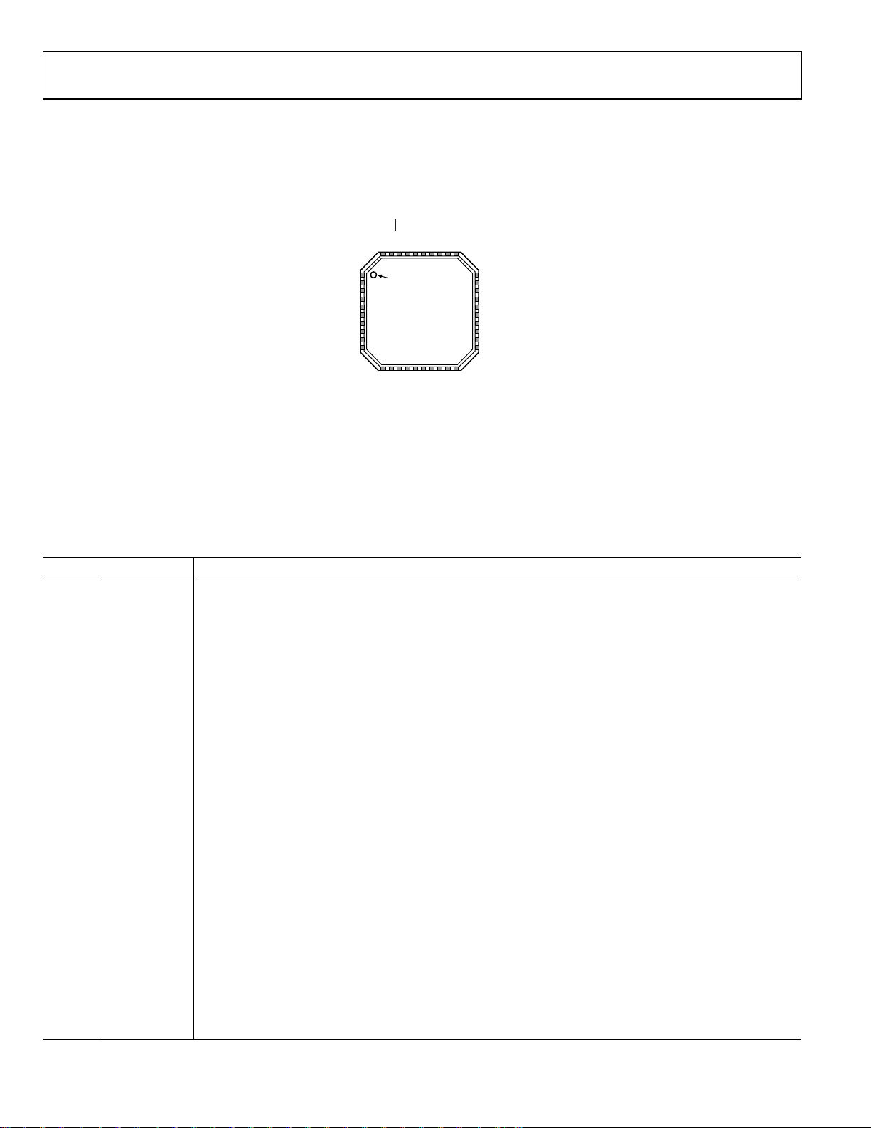
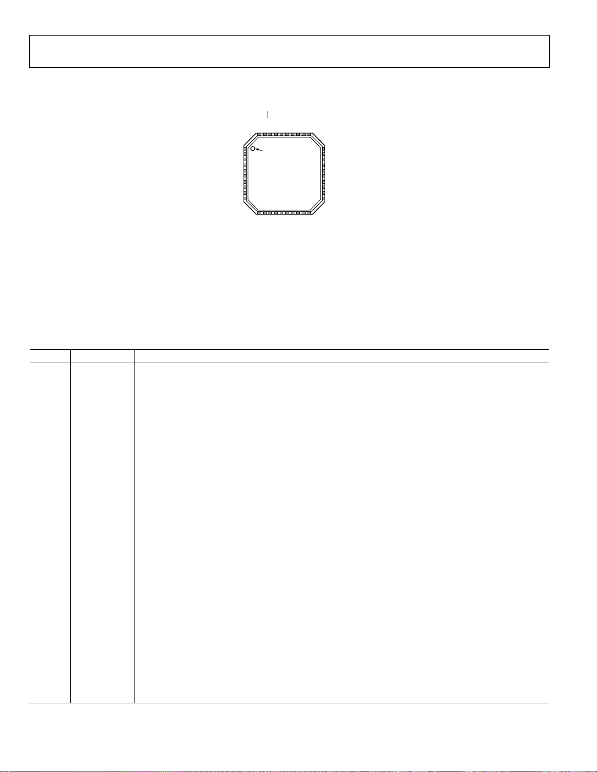
Small footprint 40-lead LFCSP RoHS-compliant package
APPLICATIONS
Wireless infrastructures
Picocell, femtocell base stations
Medical instrumentation
Ultrasound transducer excitation
Portable instrumentation
Signal generators, arbitrary waveform generators
TxDAC Digital-to-Analog Converters
AD9114/AD9115/AD9116/AD9117
GENERAL DESCRIPTION
The AD9114/AD9115/AD9116/AD9117 are pin-compatible
dual, 8-/10-/12-/14-bit, low power digital-to-analog converters
(DACs) that provide a sample rate of 125 MSPS. These TxDAC®
converters are optimized for the transmit signal path of communication systems. All the devices share the same interface, package,
and pinout, providing an upward or downward component
selection path based on performance, resolution, and cost.
The AD9114/AD9115/AD9116/AD9117 offer exceptional ac and
dc performance and support update rates up to 125 MSPS.
The flexible power supply operating range of 1.8 V to 3.3 V and
low power dissipation of the AD9114/AD9115/AD9116/AD9117
make them well suited for portable and low power applications.
PRODUCT HIGHLIGHTS
1. Low Power. DACs operate on a single 1.8 V to 3.3 V supply;
total power consumption reduces to 225 mW at 100 MSPS.
Sleep and power-down modes are provided for low power
idle periods.
2. CMOS Clock Input. High speed, single-ended CMOS clock
input supports a 125 MSPS conversion rate.
3. Easy Interfacing to Other Components. Adjustable output
common mode from 0 V to 1.2 V allows for easy interfacing
to other components that accept common-mode levels
greater than 0 V.
Rev. A
Information furnished by Analog Devices is believed to be accurate and reliable. However, no
responsibility is assumed by Analog Devices for its use, nor for any infringements of patents or other
rights of third parties that may result from its use. Specifications subject to change without notice. No
license is granted by implication or otherwise under any patent or patent rights of Analog Devices.
Trademarks and registered trademarks are the property of their respective owners.
One Technology Way, P.O. Box 9106, Norwood, MA 02062-9106, U.S.A.
Tel: 781.329.4700 www.analog.com
Fax: 781.461.3113 ©2008–2009 Analog Devices, Inc. All rights reserved.

AD9114/AD9115/AD9116/AD9117
TABLE OF CONTENTS
Features .............................................................................................. 1
Applications ....................................................................................... 1
General Description ......................................................................... 1
Product Highlights ........................................................................... 1
Revision History ............................................................................... 3
Functional Block Diagram .............................................................. 4
Specifications ..................................................................................... 5
DC Specifications ......................................................................... 5
Digital Specifications ................................................................... 7
AC Specifications .......................................................................... 8
Absolute Maximum Ratings ............................................................ 9
Thermal Resistance ...................................................................... 9
ESD Caution .................................................................................. 9
Pin Configurations and Function Descriptions ......................... 10
Typical Performance Characteristics ........................................... 18
Terminolog y .................................................................................... 31
Theory of Operation ...................................................................... 32
Serial Peripheral Interface (SPI) ................................................... 33
General Operation of the Serial Interface ............................... 33
Instruction Byte .......................................................................... 33
Serial Interface Port Pin Descriptions ..................................... 33
MSB/LSB Transfers..................................................................... 34
Serial Port Operation ................................................................. 34
Pin Mode ..................................................................................... 34
SPI Register Map ............................................................................. 35
SPI Register Descriptions .............................................................. 36
Digital Interface Operation ........................................................... 40
Digital Data Latching and Retimer Section ............................ 41
Estimating the Overall DAC Pipeline Delay........................... 42
Reference Operation .................................................................. 43
Reference Control Amplifier .................................................... 43
DAC Transfer Function ............................................................. 43
Analog Output ............................................................................ 44
Self-Calibration ........................................................................... 44
Coarse Gain Adjustment ........................................................... 45
Using the Internal Termination Resistors ............................... 46
Applications Information .............................................................. 47
Output Configurations .............................................................. 47
Differential Coupling Using a Transformer ............................... 47
Single-Ended Buffered Output Using an Op Amp ................ 47
Differential Buffered Output Using an Op Amp .................. 48
Auxiliary DACs ........................................................................... 48
DAC-to-Modulator Interfacing ................................................ 49
Correcting for Nonideal Performance of Quadrature
Modulators on the IF-to-RF Conversion ................................ 49
I/Q Channel Gain Matching ..................................................... 49
LO Feedthrough Compensation .............................................. 50
Results of Gain and Offset Correction .................................... 50
Modifying the Evaluation Board to Use the ADL5370 On-Board
Quadrature Modulator ................................................................ 51
Evaluation Board Schematics and Artwork ................................ 52
Schematics ................................................................................... 52
Silkscreens ................................................................................... 60
Bill of Materials ............................................................................... 75
Outline Dimensions ....................................................................... 78
Ordering Guide .......................................................................... 78
Rev. A | Page 2 of 80

AD9114/AD9115/AD9116/AD9117
REVISION HISTORY
3/09—Rev. 0 to Rev. A
Changes to Product Title and General Description Section ....... 1
Changes to Figure 1 ........................................................................... 4
Changed I
= 2 mA to I
OUTFS
= 20 mA..................................... 5
xOUTFS
Changes to Table 1 ............................................................................ 6
Changed I
= 2 mA to I
OUTFS
= 20 mA..................................... 7
xOUTFS
Changes to Table 2 ............................................................................ 7
Changed DVDDIO = 1.8 V to DVDDIO = 3.3 V, Table 3 and
CVDD = 3.3 V to CVDD = 1.8 V, Table 4 ..................................... 8
Changes to Table 5 and Table 6 ....................................................... 9
Changes to Table 7 .......................................................................... 10
Changes to Table 8 .......................................................................... 12
Changes to Table 9 .......................................................................... 14
Changes to Table 10 ........................................................................ 16
Changes to Typical Performance Characteristics Section ......... 18
Changes to Theory of Operation Section and Figure 84 ........... 32
Added Figure 85 to Figure 88; Renumbered Sequentially ......... 34
Changes to Table 13 ........................................................................ 35
Changes to Table 14 ........................................................................ 36
Changes to Digital Interface Operation Section and Figure 89,
Figure 90, Figure 91, Figure 92, and Figure 93 ............................ 40
Changes to Figure 94, Digital Data Latching Section, and
Retimer Section ............................................................................... 41
Added Reference Operation Section, Reference Control
Amplifier Section, DAC Transfer Function Section, Figure 96,
and Table 17 ..................................................................................... 43
Added Analog Output Section ...................................................... 44
Changes to Auxiliary DACs Section ............................................. 48
Changes to DAC to Modulator Interfacing Section, Figure 107,
and Figure 108 ................................................................................. 49
Added Figure 111 to Figure 133 .................................................... 52
Added Table 18 ................................................................................ 75
8/08—Revision 0: Initial Version
Rev. A | Page 3 of 80
AD9114/AD9115/AD9116/AD9117
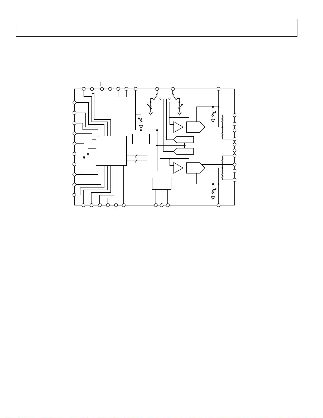
FUNCTIONAL BLOCK DIAGRAM
DB12
DB13 (MSB)
CS/PW RDN
SDIO/FORMAT
SCLK/CLKMD
RESET/PINMD
REFIO
FSADJQ/AUXQ
FSADJI/AUXI
CMLI
DB11
DB10
DB9
DB8
DVDDIO
DVSS
DVDD
DB7
DB6
DB5
1.8V
LDO
DB4
INTERLEAVED
INTERFACE
DB3
DB2
SPI
INTERFACE
1 INTO 2
DATA
DB1
(LSB) DB0
I
REF
100µA
DCLKIO
1V
QR
BAND
GAP
I DATA
Q DATA
SET
2kΩ
10kΩ
CLOCK
DIST
CVDD
CLKIN
CVSS
IR
SET
2kΩ
AUX1DAC
AUX2DAC
AD9117
60Ω TO
I DAC
Q DAC
60Ω TO
IR
260Ω
QR
260Ω
CM
CM
CMLQ
62.5Ω
62.5Ω
62.5Ω
62.5Ω
RLIN
IOUTN
IOUTP
RLIP
AVDD
AVSS
RLQP
QOUTP
QOUTN
RLQN
07466-001
Figure 1.
Rev. A | Page 4 of 80

AD9114/AD9115/AD9116/AD9117
SPECIFICATIONS
DC SPECIFICATIONS
T
to T
MIN
, AVDD = 3.3 V, DVDD = 1.8 V, DVDDIO = 3.3 V, CVDD = 3.3 V, I
MAX
Table 1.
AD9114 AD9115 AD9116 AD9117
Parameter
RESOLUTION 8 10 12 14 Bits
ACCURACY, AVDD = DVDDIO =
CVDD = 3.3 V
Differential Nonlinearity (DNL)
Precalibration ±0.02 ±0.06 ±0.4 ±1.4 LSB
Postcalibration ±0.02 ±0.04 ±0.2 ±0.6 LSB
Integral Nonlinearity (INL)
Precalibration ±0.03 ±0.19 ±0.68 ±1.2 LSB
Postcalibration ±0.03 ±0.07 ±0.42 ±0.6 LSB
ACCURACY, AVDD = DVDDIO =
CVDD = 1.8 V
Differential Nonlinearity (DNL)
Precalibration ±0.02 ±0.08 ±0.5 ±1.8 LSB
Postcalibration ±0.01 ±0.06 ±0.2 ±1.0 LSB
Integral Nonlinearity (INL)
Precalibration ±0.04 ±0.2 ±0.5 ±1.8 LSB
Postcalibration ±0.02 ±0.1 ±0.3 ±1.1 LSB
MAIN DAC OUTPUTS
Offset Error −1 +1 −1 +1 −1 +1 −1 +1 mV
Gain Error Internal Reference −2 +2 −2 +2 −2 +2 −2 +2 % of FSR
Full-Scale Output Current1
AVDD = 3.3 V 2 8 20 2 8 20 2 8 20 2 8 20 mA
AVDD = 1.8 V 2 8 2 8 2 8 2 8 mA
Output Common-Mode Level
(8 mA CMLx Pin)
Output Resistance 200 200 200 200 MΩ
Crosstalk, Q DAC to I DAC
(f
= 30 MHz)
OUT
Crosstalk, Q DAC to I DAC
(f
= 60 MHz)
OUT
MAIN DAC TEMPERATURE DRIFT
Offset 0 0 0 0 ppm/°C
Gain ±40 ±40 ±40 ±40 ppm/°C
Reference Voltage ±25 ±25 ±25 ±25 ppm/°C
AUXDAC OUTPUTS
Resolution 10 10 10 10 Bits
Full-Scale Output Current
(Current Sourcing Mode)
Voltage Output Mode
Output Compliance Range
(Sourcing 1 mA)
Output Compliance Range
(Sinking 1 mA)
Output Resistance in Current
Output Mode AV
to 1 V
SS
AUXDAC Monotonicity
Guaranteed
−0.5 0 +1.2 −0.5 0 +1.2 −0.5 0 +1.2 −0.5 0 +1.2 V
95 95 95 95 dB
76 76 76 76 dB
125 125 125 125 μA
VSS VDD −
VSS VDD −
0.25
VSS +
V
0.25
VSS +
DD
V
0.25
1 1 1 1 MΩ
10 10 10 10 Bits
= 20 mA, maximum sample rate, unless otherwise noted.
xOUTFS
VSS VDD −
0.25
VSS +
DD
0.25
V
VSS VDD −
0.25
VSS +
DD
0.25
0.25
V
DD
Unit Min Typ Max Min Typ Max Min Typ Max Min Typ Max
V
V
Rev. A | Page 5 of 80
AD9114/AD9115/AD9116/AD9117
AD9114 AD9115 AD9116 AD9117
Parameter
REFERENCE OUTPUT
Internal Reference Voltage 0.98 1.025 1.08 0.98 1.025 1.08 0.98 1.025 1.08 0.98 1.025 1.08 V
Output Resistance 10 10 10 10 kΩ
REFERENCE INPUT
Voltage Compliance
AVDD = 3.3 V 0.1 1.25 0.1 1.25 0.1 1.25 0.1 1.25 V
AVDD = 1.8 V 0.1 1.0 0.1 1.0 0.1 1.0 0.1 1.0 V
Input Resistance External
1 1 1 1 MΩ
Reference Mode
DAC MATCHING
Gain Matching −1 +1 −1 +1 −1 +1 −1 +1 % of FSR
ANALOG SUPPLY VOLTAGES
AVDD 1.7 3.5 1.7 3.5 1.7 3.5 1.7 3.5 V
CVDD 1.7 3.5 1.7 3.5 1.7 3.5 1.7 3.5 V
DIGITAL SUPPLY VOLTAGES
DVDD 1.7 1.9 1.7 1.9 1.7 1.9 1.7 1.9 V
DVDDIO 1.7 3.5 1.7 3.5 1.7 3.5 1.7 3.5 V
POWER CONSUMPTION, AVDD =
DVDDIO = CVDD = 3.3 V
f
= 125 MSPS, IF = 12.5 MHz 220 220 220 220 mW
DAC
I
55 55 55 55 mA
AVDD
I
+ I
DVDD
I
CVDD
10 10 10 10 mA
DVDDIO
3 3 3 3 mA
Power-Down Mode with Clock 8.5 8.5 8.5 8.5 mW
Power-Down Mode No Clock 3 3 3 3 mW
Power Supply Rejection Ratio −0.009 −0.009 −0.009 −0.009 % FSR/V
POWER CONSUMPTION, AVDD =
DVDDIO = CVDD = 1.8 V
f
= 125 MSPS, IF = 12.5 MHz 58 58 58 58 mW
DAC
I
24 24 24 24 mA
AVDD
I
DVDD + IDVDDIO
I
CVDD
8 8 8 8 mA
2 2 2 2 mA
Power-Down Mode with Clock 12 12 12 12 mW
Power-Down Mode No Clock 850 850 850 850 μW
Power Supply Rejection Ratio −0.007 −0.007 −0.007 −0.007 % FSR/V
OPERATING RANGE −40 +25 +85 −40 +25 +85 −40 +25 +85 −40 +25 +85 °C
1
Based on a 10 kΩ external resistor.
Unit Min Typ Max Min Typ Max Min Typ Max Min Typ Max
Rev. A | Page 6 of 80

AD9114/AD9115/AD9116/AD9117
DIGITAL SPECIFICATIONS
T
to T
MIN
, AVDD = 3.3 V, DVDD = 1.8 V, DVDDIO = 3.3 V, CVDD = 3.3 V, I
MAX
Table 2.
Parameter Min Typ Max Unit
DAC CLOCK INPUT (CLKIN)
VIH 2.1 3 V
VIL 0 0.9 V
Maximum Clock Rate 125 MSPS
SERIAL PERIPHERAL INTERFACE
Maximum Clock Rate (SCLK) 25 MHz
Minimum Pulse Width High 20 ns
Minimum Pulse Width Low 20 ns
INPUT DATA
1.8 V Q Channel or DCLKIO Falling Edge
Setup 0.25 ns
Hold 1.2 ns
1.8 V I Channel or DCLKIO Rising Edge
Setup 0.13 ns
Hold 1.1 ns
3.3 V Q Channel or DCLKIO Falling Edge
Setup −0.2 ns
Hold 1.5 ns
3.3 V I Channel or DCLKIO Rising Edge
Setup −0.2 ns
Hold 1.6 ns
VIH 2.1 3 V
VIL 0 0.9 V
= 20 mA, maximum sample rate, unless otherwise noted.
xOUTFS
Rev. A | Page 7 of 80
AD9114/AD9115/AD9116/AD9117
AC SPECIFICATIONS
T
to T
MIN
, AVDD = 3.3 V, DVDD = 1.8 V, DVDDIO = 3.3 V, CVDD = 3.3 V, I
MAX
Table 3.
Parameter
SPURIOUS FREE DYNAMIC RANGE
(SFDR)
f
= 125 MSPS, f
DAC
f
= 125 MSPS, f
DAC
= 10 MHz 76 85 85 85 dBc
OUT
= 50 MHz 55 55 55 55 dBc
OUT
TWO TONE INTERMODULATION
DISTORTION (IMD)
f
= 125 MSPS, f
DAC
f
= 125 MSPS, f
DAC
= 10 MHz 81 81 81 82 dBc
OUT
= 50 MHz 60 60 60 61 dBc
OUT
NOISE SPECTRAL DENSITY (NSD),
EIGHT-TONE, 500 kHz TONE SPACING
f
= 125 MSPS, f
DAC
f
= 125 MSPS, f
DAC
= 10 MHz −132 −143 −153 −157 dBc/Hz
OUT
= 50 MHz −128 −138 −146 −149 dBc/Hz
OUT
W-CDMA ADJACENT CHANNEL LEAKAGE
RATIO (ACLR), SINGLE CARRIER
f
= 61.44 MSPS, f
DAC
f
= 122.88 MSPS, f
DAC
= 20 MHz −78 −78 −78 −78 dBc
OUT
= 30 MHz −80 −80 −80 −80 dBc
OUT
AD9114 AD9115 AD9116 AD9117
= 20 mA, maximum sample rate, unless otherwise noted.
xOUTFS
Unit Min Typ Max Min Typ Max Min Typ Max Min Typ Max
T
to T
MIN
, AVDD = 1.8 V, DVDD = 1.8 V, DVDDIO = 1.8 V, CVDD = 1.8 V, I
MAX
Table 4.
Parameter
SPURIOUS FREE DYNAMIC RANGE
(SFDR)
f
= 125 MSPS, f
DAC
f
= 125 MSPS, f
DAC
= 10 MHz 73 76 76 76 dBc
OUT
= 50 MHz 48 48 48 48 dBc
OUT
TWO TONE INTERMODULATION
DISTORTION (IMD)
f
= 125 MSPS, f
DAC
f
= 125 MSPS, f
DAC
= 10 MHz 76 76 76 76 dBc
OUT
= 50 MHz 50 50 50 50 dBc
OUT
NOISE SPECTRAL DENSITY (NSD),
EIGHT-TONE, 500 kHz TONE SPACING
f
= 125 MSPS, f
DAC
f
= 125 MSPS, f
DAC
= 10 MHz −125 −136 −146 −150 dBc/Hz
OUT
= 50 MHz −117 −127 −135 −138 dBc/Hz
OUT
W-CDMA ADJACENT CHANNEL LEAKAGE
RATIO (ACLR), SINGLE CARRIER
f
= 61.44 MSPS, f
DAC
f
= 122.88 MSPS, f
DAC
= 20 MHz −69 −69 −69 −69 dBc
OUT
= 30 MHz −72 −72 −72 −72 dBc
OUT
= 8 mA, maximum sample rate, unless otherwise noted.
xOUTFS
AD9114 AD9115 AD9116 AD9117
Unit Min Typ Max Min Typ Max Min Typ Max Min Typ Max
Rev. A | Page 8 of 80
AD9114/AD9115/AD9116/AD9117
ABSOLUTE MAXIMUM RATINGS
Table 5.
Parameter Rating
AVDD, DVDDIO, CVDD to AVSS,
−0.3 V to +3.9 V
DVSS, CVSS
DVDD to DVSS −0.3 V to +2.1 V
AVSS to DVSS, CVSS −0.3 V to +0.3 V
DVSS to AVSS, CVSS −0.3 V to +0.3 V
CVSS to AVSS, DVSS −0.3 V to +0.3 V
REFIO, FSADJQ, FSADJI, CMLQ,
−0.3 V to AVDD + 0.3 V
CMLI to AVSS
QOUTP, QOUTN, IOUTP, IOUTN,
−1.0 V to AVDD + 0.3 V
RLQP, RLQN, RLIP, RLIN to AVSS
DBn1 (MSB) to D0 (LSB), CS, SCLK,
−0.3 V to DVDDIO + 0.3 V
SDIO, RESET to DVSS
CLKIN to CVSS −0.3 V to CVDD + 0.3 V
Junction Temperature 125°C
Storage Temperature Range −65°C to +150°C
1
n stands for 7 for the AD9114, 9 for the AD9115, 11 for the AD9116, and 13
for the AD9117.
Stresses above those listed under Absolute Maximum Ratings
may cause permanent damage to the device. This is a stress
rating only; functional operation of the device at these or any
other conditions above those indicated in the operational
section of this specification is not implied. Exposure to absolute
maximum rating conditions for extended periods may affect
device reliability.
THERMAL RESISTANCE
Table 6.
Package Type θJA θ
40-Lead LFCSP (with No Airflow
29.8
Movement)
1
These calculations are intended to represent the thermal performance of the
indicated packages using a JEDEC multilayer test board. Do not assume the
same level of thermal performance in actual applications without a careful
inspection of the conditions in the application to determine that they are
similar to those assumed in these calculations.
1
1
θ
JB
Unit
JC
19.0 3.4 °C/W
ESD CAUTION
Rev. A | Page 9 of 80
AD9114/AD9115/AD9116/AD9117
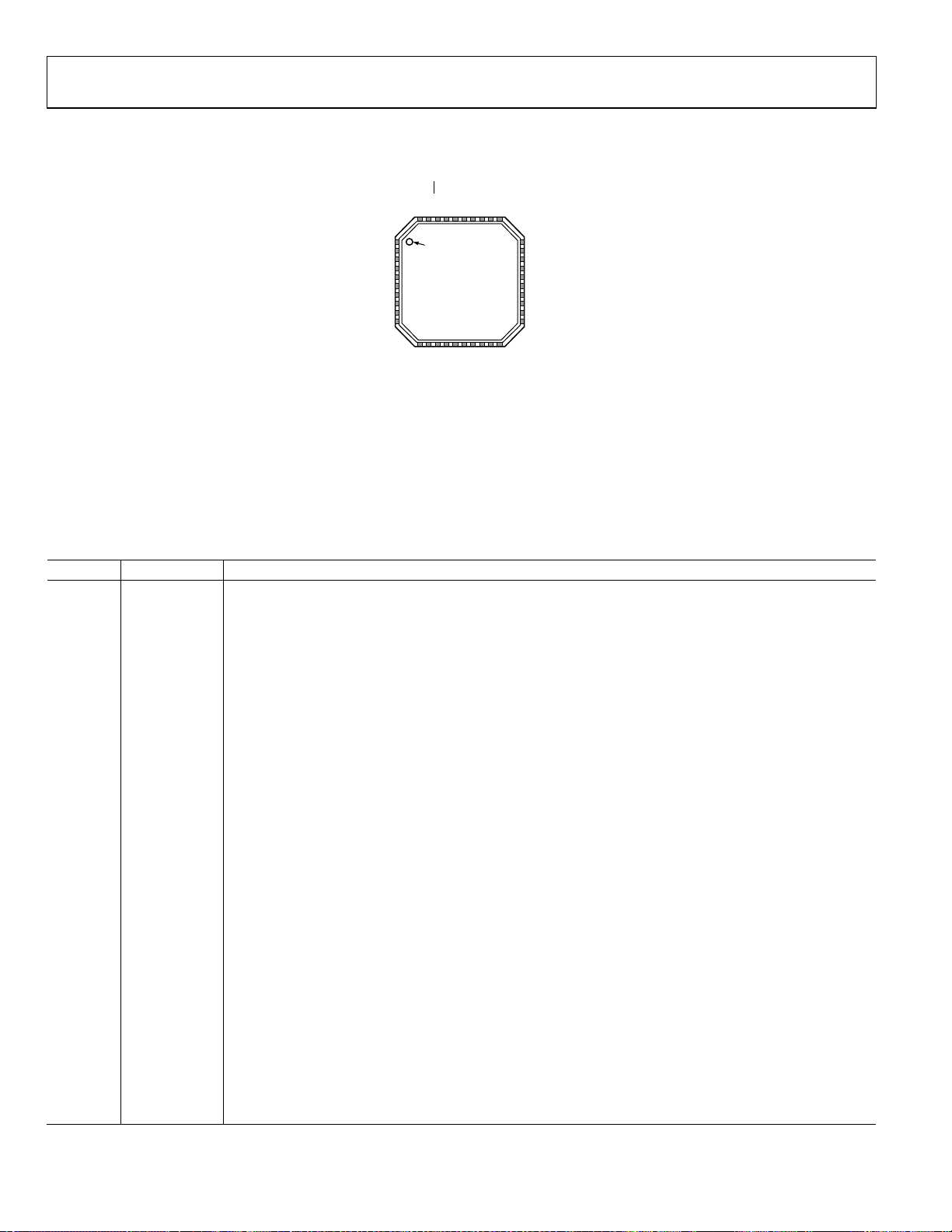
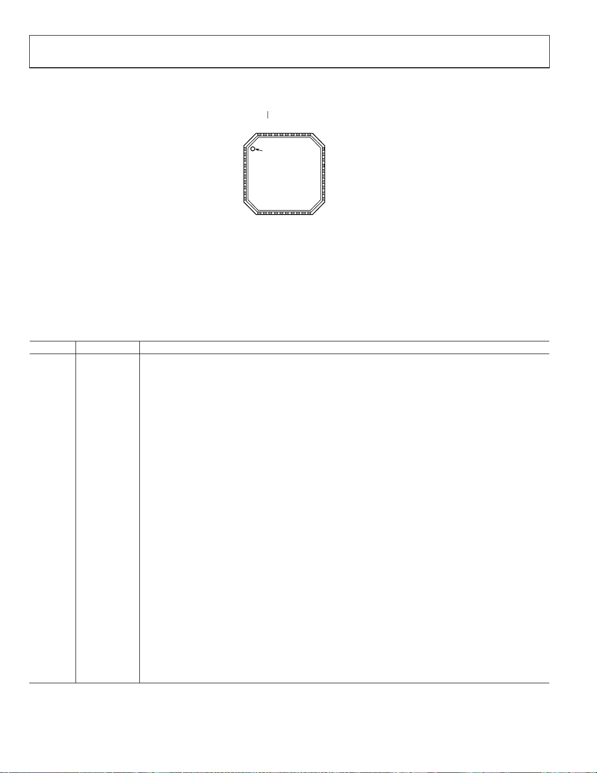
Q
PIN CONFIGURATIONS AND FUNCTION DESCRIPTIONS
X
RDN
W
(MSB)
DIO/FORMAT
S
CS/P
DB7
DB6
37
38
39
40
PIN 1
1DB5
INDICATOR
2DB4
3DB3
4DB2
5DVDDIO
6DVSS
7DVDD
8DB1
9DB0 (LSB)
10NC
NOTES
1. NC = NO CO NNECT
2. THE EXPO SED PAD IS CONNECTED TO AVSS AND
MUST BE SOL DERED TO THE GROUND PLANE.
EXPOSED METAL AT PACKAGE CO RNERS IS
CONNECTED TO THIS PAD.
AD9114
TOP VIEW
(Not to Scale)
11
12
13
14
C
NC
NC
NC
N
Figure 2. AD9114 Pin Configuration
CMLI
FSADJI/AUXI
REFIO
RESET/PINMD
SCLK/CLKMD
FSADJQ/AU
31
32
33
34
35
36
30
RLIN
29
IOUTN
28
IOUTP
27
RLIP
26
AVD D
25
AVS S
24
RLQP
23
QOUTP
22
QOUTN
21
RLQN
15
17
16
18
19
20
NC
CVSS
CVDD
CMLQ
CLKIN
DCLKIO
07466-005
Table 7. AD9114 Pin Function Descriptions
Pin No. Mnemonic Description
1 to 4 DB[5:2] Digital Inputs.
5 DVDDIO Digital I/O Supply Voltage Input (1.8 V to 3.3 V Nominal).
6 DVSS Digital Common.
7 DVDD
Digital Core Supply Voltage Output (1.8 V). Strap DVDD to DVDDIO at 1.8 V. If DVDDIO > 1.8 V, bypass DVDD
with a 1.0 μF capacitor; however, do not otherwise connect it. The LDO should not drive external loads.
8 DB1 Digital Inputs
9 DB0 (LSB) Digital Input (LSB).
10 to
NC No Connect. These pins are not connected to the chip.
15
16 DCLKIO Data Input/Output Clock. Clock used to qualify input data.
17 CVDD Sampling Clock Supply Voltage Input (1.8 V to 3.3 V). CVDD must be ≥ DVDD.
18 CLKIN LVCMOS Sampling Clock Input.
19 CVSS Sampling Clock Supply Voltage Common.
20 CMLQ
Q DAC Output Common-Mode Level. When the internal on-chip (QR
the on-chip QR
resistor. It is recommended to leave this pin unconnected. When the internal on-chip (QR
CML
) is enabled, this pin is connected to
CML
disabled, this pin is the common-mode load for Q DAC and must be connected to AVSS through a resistor, see
the Using the Internal Termination Resistors section. Recommended value for this external resistor is 0 Ω.
21 RLQN
Load Resistor (62.5 Ω) to the CMLQ Pin. For the internal load resistor to be used, this pin should be tied to
QOUTN externally.
22 QOUTN Complementary Q DAC Current Output. Full-scale current is sourced when all data bits are 0s.
23 QOUTP Q DAC Current Output. Full-scale current is sourced when all data bits are 1s.
24 RLQP
Load Resistor (62.5 Ω) to the CMLQ Pin. For the internal load resistor to be used, this pin should be tied to
QOUTP externally.
25 AVSS Analog Common.
26 AVDD Analog Supply Voltage Input (1.8 V to 3.3 V).
27 RLIP
Load Resistor (62.5 Ω) to the CMLI Pin. For the internal load resistor to be used, this pin should be tied to
IOUTP externally.
28 IOUTP I DAC Current Output. Full-scale current is sourced when all data bits are 1s.
CML
) is
Rev. A | Page 10 of 80
AD9114/AD9115/AD9116/AD9117
Pin No. Mnemonic Description
29 IOUTN Complementary I DAC Current Output. Full-scale current is sourced when all data bits are 0s.
30 RLIN
31 CMLI
32 FSADJQ/AUXQ
Auxiliary Q DAC Output (AUXQ). When the internal on-chip (QR
33 FSADJI/AUXI
Auxiliary I DAC Output (AUXI). When the internal on-chip (IR
34 REFIO
35 RESET/PINMD
A logic high (pull-up to DVDDIO) puts the device into pin mode (PINMD).
36 SCLK/CLKMD Clock Input for Serial Port (SCLK). In SPI mode, this pin is the clock input for the serial port.
37 SDIO/FORMAT Serial Port Input/Output (SDIO). In SPI mode, this pin is the bidirectional data line for the serial port.
38
/PWRDN Active Low Chip Select (CS). In SPI mode, this pin serves as the active low chip select.
CS
39 DB7 (MSB) Digital Input (MSB).
40 DB6 Digital Input.
EP (EPAD)
Load Resistor (62.5 Ω) to the CMLI Pin. For the internal load resistor to be used, this pin should be tied to
IOUTN externally.
I DAC Output Common-Mode Level. When the internal on-chip (IR
on-chip IR
resistor. It is recommended to leave this pin unconnected. When the internal on-chip (IR
CML
) is enabled, this pin is connected to the
CML
CML
) is
disabled, this pin is the common-mode load for I DAC and must be connected to AVSS through a resistor, see
the Using the Internal Termination Resistors section. Recommended value for this external resistor is 0 Ω.
Full-Scale Current Output Adjust (FSADJQ). When the internal on chip (QR
) is disabled, this pin is the full-scale
SET
current output adjust for Q DAC and must be connected to AVSS through a resistor, see the Theory of Operation
section. Nominal value for this external resistor is 4 kΩ for 8 mA output current.
) is enabled, this pin is the auxiliary Q DAC output.
SET
Full-Scale Current Output Adjust (FSADJI). When the internal on-chip (IR
) is disabled, this pin is the full-scale
SET
current output adjust for I DAC and must be connected to AVSS through a resistor, see the Theory of Operation
section. Nominal value for this external resistor is 4 kΩ for 8 mA output current.
) is enabled, it is the auxiliary I DAC output.
SET
Reference Input/Output. Serves as a reference input when the internal reference is disabled. Provides a 1.0 V
reference output when in internal reference mode (a 0.1 μF capacitor to AVSS is required).
This pin defines the operation mode of the part. A logic low (pull-down to DVSS) sets the part in SPI mode.
Pulse RESET high to reset the SPI registers to their default values.
Clock Mode (CLKMD). In pin mode, CLKMD determines the phase of the internal retiming clock. When
DCLKIO = CLKIN, tie it to 0. When DCLKIO ≠ CLKIN, pulse 0 to 1 to edge trigger the internal retimer, see
the Retimer section.
Format Pin (FORMAT). In pin mode, FORMAT determines the data format of digital data. A logic low (pull-down
to DVSS) selects the binary input data format. A logic high (pull-up to DVDDIO) selects the twos complement
input data format.
Power-Down (PWRDN). In pin mode, a logic high (pull-up to DVDDIO) powers down the device, except for
the SPI port.
The exposed pad is connected to AVSS and must be soldered to the ground plane. Exposed metal at the
package corners is connected to this pad.
Rev. A | Page 11 of 80
AD9114/AD9115/AD9116/AD9117
Q
2
LKMD
ORMAT
RDN
CS/PW
DB9 (MSB)
DB8
38
39
40
PIN 1
1DB7
INDICATOR
2DB6
3DB5
4DB4
5DVDDIO
6DVSS
7DVDD
8DB3
9DB2
10DB1
NOTES
1. NC = NO CONNECT
. THE EXPO SED PAD IS CONNECT ED TO AVSS AND
MUST BE SOLDERED TO THE GROUND PLANE.
EXPOSED METAL AT PACKAGE CO RNERS IS
CONNECTED TO THIS PAD.
AD9115
TOP VIEW
(Not to Scale)
11
12
13
NC
NC
DB0 (LSB)
Figure 3. AD9115 Pin Configuration
Q/AUX
MLI
C
FSADJI/AUXI
REFIO
RESET/PINMD
SCLK/C
SDIO/F
FSADJ
31
32
33
34
35
36
37
30 RLIN
29 IOUT N
28 IOUTP
27 RLIP
26 AVDD
25 AVSS
24 RLQP
23 QOUTP
22 QOUTN
21 RLQ N
15
17
16
18
19
14
NC
20
NC
VDD
CVSS
C
CMLQ
CLKIN
DCLKIO
07466-004
Table 8. AD9115 Pin Function Description
Pin No. Mnemonic Description
1 to 4 DB[7:4] Digital Inputs.
5 DVDDIO Digital I/O Supply Voltage Input (1.8 V to 3.3 V Nominal).
6 DVSS Digital Common.
7 DVDD
Digital Core Supply Voltage Output (1.8 V). Strap DVDD to DVDDIO at 1.8 V. If DVDDIO > 1.8 V, bypass DVDD
with a 1.0 μF capacitor; however, do not otherwise connect it. The LDO should not drive external loads.
8 to 10 DB[3:1] Digital Inputs.
11 DB0 (LSB) Digital Input (LSB).
12 to 15 NC No Connect. These pins are not connected to the chip.
16 DCLKIO Data Input/Output Clock. Clock used to qualify input data.
17 CVDD Sampling Clock Supply Voltage Input (1.8 V to 3.3 V). CVDD must be ≥ DVDD.
18 CLKIN LVCMOS Sampling Clock Input.
19 CVSS Sampling Clock Supply Voltage Common.
20 CMLQ
Q DAC Output Common-Mode Level. When the internal on-chip (QR
the on-chip QR
resistor. It is recommended to leave this pin unconnected. When the internal on-chip (QR
CML
) is enabled, this pin is connected to
CML
disabled, this pin is the common-mode load for Q DAC and must be connected to AVSS through a resistor, see
the Using the Internal Termination Resistors section. Recommended value for this external resistor is 0 Ω.
21 RLQN
Load Resistor (62.5 Ω) to the CMLQ Pin. For the internal load resistor to be used, this pin should be tied to
QOUTN externally.
22 QOUTN Complementary Q DAC Current Output. Full-scale current is sourced when all data bits are 0s.
23 QOUTP Q DAC Current Output. Full-scale current is sourced when all data bits are 1s.
24 RLQP
Load Resistor (62.5 Ω) to the CMLQ Pin. For the internal load resistor to be used, this pin should be tied to
QOUTP externally.
25 AVSS Analog Common.
26 AVDD Analog Supply Voltage Input (1.8 V to 3.3 V).
27 RLIP
Load Resistor (62.5 Ω) to the CMLI Pin. For the internal load resistor to be used, this pin should be tied to
IOUTP externally.
28 IOUTP I DAC Current Output. Full-scale current is sourced when all data bits are 1s.
29 IOUTN Complementary I DAC Current Output. Full-scale current is sourced when all data bits are 0s.
30 RLIN
Load Resistor (62.5 Ω) to the CMLI Pin. For the internal load resistor to be used, this pin should be tied to
IOUTN externally.
CML
) is
Rev. A | Page 12 of 80
AD9114/AD9115/AD9116/AD9117
Pin No. Mnemonic Description
31 CMLI
I DAC Output Common-Mode Level. When the internal on-chip (IR
on-chip IR
resistor. It is recommended to leave this pin unconnected. When the internal on-chip (IR
CML
disabled, this pin is the common-mode load for I DAC and must be connected to AVSS through a resistor,
see the Using the Internal Termination Resistors section. Recommended value for this external resistor is 0 Ω.
32 FSADJQ/AUXQ
Full-Scale Current Output Adjust (FSADJQ). When the internal on chip (QR
scale current output adjust for Q DAC and must be connected to AVSS through a resistor, see the Theory of
Operation section. Nominal value for this external resistor is 4 kΩ for 8 mA output current.
Auxiliary Q DAC Output (AUXQ). When the internal on-chip (QR
33 FSADJI/AUXI
Full-Scale Current Output Adjust (FSADJI). When the internal on-chip (IR
SET
current output adjust for I DAC and must be connected to AVSS through a resistor, see the Theory of Operation
section. Nominal value for this external resistor is 4 kΩ for 8 mA output current.
Auxiliary I DAC Output (AUXI). When the internal on-chip (IR
34 REFIO
Reference Input/Output. Serves as a reference input when the internal reference is disabled. Provides a 1.0 V
SET
reference output when in internal reference mode (a 0.1 μF capacitor to AVSS is required).
35 RESET/PINMD
This pin defines the operation mode of the part. A logic low (pull-down to DVSS) sets the part in SPI mode.
Pulse RESET high to reset the SPI registers to their default values.
A logic high (pull-up to DVDDIO) puts the device into pin mode (PINMD).
36 SCLK/CLKMD Clock Input for Serial Port (SCLK). In SPI mode, this pin is the clock input for the serial port.
Clock Mode (CLKMD). In pin mode, CLKMD determines the phase of the internal retiming clock. When
DCLKIO = CLKIN, tie it to 0. When DCLKIO ≠ CLKIN, pulse 0 to 1 to edge trigger the internal retime, see
the Retimer section.
37 SDIO/FORMAT Serial Port Input/Output (SDIO). In SPI mode, this pin is the bidirectional data line for the serial port.
Format Pin (FORMAT). In pin mode, FORMAT determines the data format of digital data. A logic low (pull-down
to DVSS) selects the binary input data format. A logic high (pull-up to DVDDIO) selects the twos complement
input data format.
38
/PWRDN Active Low Chip Select (CS). In SPI mode, this pin serves as the active low chip select.
CS
Power-Down (PWRDN). In pin mode, a logic high (pull-up to DVDDIO) powers down the device, except for the
SPI port.
39 DB9 (MSB) Digital Input (MSB).
40 DB82 Digital Input.
EP (EPAD)
The exposed pad is connected to AVSS and must be soldered to the ground plane. Exposed metal at the
package corners is connected to this pad.
) is enabled, this pin is connected to the
CML
) is disabled, this pin is the full-
SET
CML
) is
) is enabled, this pin is the auxiliary Q DAC output.
) is disabled, this pin is the full-scale
SET
) is enabled, it is the auxiliary I DAC output.
Rev. A | Page 13 of 80
AD9114/AD9115/AD9116/AD9117
Q
2
NMD
LKMD
RDN
/C
CMLI
FSADJI/AUXI
REFIO
RESET/PI
SCLK
SDIO/FORMAT
CS/PW
DB11 (MSB)
DB10
38
39
40
PIN 1
1DB9
INDICATOR
2DB8
3DB7
4DB6
5DVDDIO
6DVSS
7DVDD
8DB5
9DB4
10DB3
NOTES
1. NC = NO CONNECT
. THE EXPOSED PAD IS CONNECTED TO AVSS AND
MUST BE SOL DERED TO THE GROUND PLANE.
EXPOSED METAL AT PACKAGE CORNERS IS
CONNECTED TO THIS PAD.
AD9116
TOP VIEW
(Not to Scale)
11
12
13
DB2
DB1
DB0 (LSB)
Figure 4. AD9116 Pin Configuration
FSADJQ/AUX
31
32
33
34
35
36
37
30 RLI N
29 IOUTN
28 IOUTP
27 RLI P
26 AVDD
25 AVSS
24 RLQ P
23 QOUTP
22 QOUTN
21 RLQ N
15
17
16
18
19
14
NC
20
S
NC
CVS
CVDD
CMLQ
CLKIN
CLKIO
D
07466-003
Table 9. AD9116 Pin Function Descriptions
Pin No. Mnemonic Description
1 to 4 DB[9:6] Digital Inputs.
5 DVDDIO Digital I/O Supply Voltage Input (1.8 V to 3.3 V Nominal).
6 DVSS Digital Common.
7 DVDD
Digital Core Supply Voltage Output (1.8 V). Strap DVDD to DVDDIO at 1.8 V. If DVDDIO > 1.8 V, bypass DVDD
with a 1.0 μF capacitor; however, do not otherwise connect it. The LDO should not drive external loads.
8 to 12 DB[5:1] Digital Inputs.
13 DB0 (LSB) Digital Input (LSB).
14, 15 NC No Connect. These pins are not connected to the chip.
16 DCLKIO Data Input/Output Clock. Clock used to qualify input data.
17 CVDD Sampling Clock Supply Voltage Input (1.8 V to 3.3 V ). CVDD must be ≥ DVDD.
18 CLKIN LVCMOS Sampling Clock Input.
19 CVSS Sampling Clock Supply Voltage Common.
20 CMLQ
Q DAC Output Common-Mode Level. When the internal on-chip (QR
the on-chip QR
resistor. It is recommended to leave this pin unconnected. When the internal on-chip (QR
CML
) is enabled, this pin is connected to
CML
disabled, this pin is the common-mode load for Q DAC and must be connected to AVSS through a resistor,
see the Using the Internal Termination Resistors section. Recommended value for this external resistor is 0 Ω.
21 RLQN
Load Resistor (62.5 Ω) to the CMLQ Pin. For the internal load resistor to be used, this pin should be tied to
QOUTN externally.
22 QOUTN Complementary Q DAC Current Output. Full-scale current is sourced when all data bits are 0s.
23 QOUTP Q DAC Current Output. Full-scale current is sourced when all data bits are 1s.
24 RLQP
Load Resistor (62.5 Ω) to the CMLQ Pin. For the internal load resistor to be used, this pin should be tied to
QOUTP externally.
25 AVSS Analog Common.
26 AVDD Analog Supply Voltage Input (1.8 V to 3.3 V).
27 RLIP
Load Resistor (62.5 Ω) to the CMLI Pin. For the internal load resistor to be used, this pin should be tied to
IOUTP externally.
28 IOUTP I DAC Current Output. Full-scale current is sourced when all data bits are 1s.
29 IOUTN Complementary I DAC Current Output. Full-scale current is sourced when all data bits are 0s.
30 RLIN
Load Resistor (62.5 Ω) to the CMLI Pin. For the internal load resistor to be used, this pin should be tied to
IOUTN externally.
CML
) is
Rev. A | Page 14 of 80

AD9114/AD9115/AD9116/AD9117
Pin No. Mnemonic Description
31 CMLI
I DAC Output Common-Mode Level. When the internal on-chip (IR
on-chip IR
resistor. It is recommended to leave this pin unconnected. When the internal on-chip (IR
CML
disabled, this pin is the common mode load for I DAC and must be connected to AVSS through a resistor, see
the Using the Internal Termination Resistors section. Recommended value for this external resistor is 0 Ω.
32 FSADJQ/AUXQ
Full-Scale Current Output Adjust (FSADJQ). When the internal on chip (QR
scale current output adjust for Q DAC and must be connected to AVSS through a resistor, see the Theory of
Operation section. Nominal value for this external resistor is 4 kΩ for 8 mA output current.
Auxiliary Q DAC Output (AUXQ). When the internal on-chip (QR
33 FSADJI/AUXI
Full-Scale Current Output Adjust (FSADJI). When the internal on-chip (IR
SET
current output adjust for I DAC and must be connected to AVSS through a resistor, see the Theory of Operation
section. Nominal value for this external resistor is 4 kΩ for 8 mA output current.
Auxiliary I DAC Output (AUXI). When the internal on-chip (IR
34 REFIO
Reference Input/Output. Serves as a reference input when the internal reference is disabled. Provides a 1.0 V
SET
reference output when in internal reference mode (a 0.1 μF capacitor to AVSS is required).
35 RESET/PINMD
This pin defines the operation mode of the part. A logic low (pull-down to DVSS) sets the part in SPI mode.
Pulse RESET high to reset the SPI registers to their default values.
A logic high (pull-up to DVDDIO) puts the device into pin mode (PINMD).
36 SCLK/CLKMD Clock Input for Serial Port (SCLK). In SPI mode, this pin is the clock input for the serial port.
Clock Mode (CLKMD). In pin mode, CLKMD determines the phase of the internal retiming clock. When
DCLKIO = CLKIN, tie it to 0. When DCLKIO ≠ CLKIN, pulse 0 to 1 to edge trigger the internal retime, see
the Retimer section.
37 SDIO/FORMAT Serial Port Input/Output (SDIO). In SPI mode, this pin is the bidirectional data line for the serial port.
Format Pin (FORMAT). In pin mode, FORMAT determines the data format of digital data. A logic low
(pull-down to DVSS) selects the binary input data format. A logic high (pull-up to DVDDIO) selects the
twos complement input data format.
38
/PWRDN Active Low Chip Select (CS). In SPI mode, this pin serves as the active low chip select.
CS
Power-Down (PWRDN). In pin mode, a logic high (pull-up to DVDDIO) powers down the device, except for
the SPI port.
39 DB11 (MSB) Digital Input (MSB).
40 DB10 Digital Input.
EP (EPAD)
The exposed pad is connected to AVSS and must be soldered to the ground plane. Exposed metal at the
package corners is connected to this pad.
) is enabled, this pin is connected to the
CML
) is disabled, this pin is the full-
SET
CML
) is
) is enabled, this pin is the auxiliary Q DAC output.
) is disabled, this pin is the full-scale
SET
) is enabled, it is the auxiliary I DAC output.
Rev. A | Page 15 of 80
AD9114/AD9115/AD9116/AD9117
Q
ORMAT
RDN
B13 (MSB)
B12
CS/PW
D
D
38
39
40
PIN 1
1DB11
INDICATOR
2DB10
3DB9
4DB8
5DVDDIO
6DVSS
7DVDD
8DB7
9DB6
10DB5
NOTES
1. THE EXPO SED PAD IS CONNECTED TO AVSS AND
MUST BE SOL DERED TO THE G ROUND PLANE.
EXPOSED METAL AT PACKAGE CO RNERS IS
CONNECTED TO THIS PAD.
AD9117
TOP VIEW
(Not to Scale)
11
12
13
DB4
DB3
DB2
Figure 5. AD9117 Pin Configuration
Table 10. AD9117 Pin Function Descriptions
Pin No. Mnemonic Description
1 to 4 DB[11:8] Digital Inputs.
5 DVDDIO Digital I/O Supply Voltage Input (1.8 V to 3.3 V Nominal).
6 DVSS Digital Common.
7 DVDD
Digital Core Supply Voltage Output (1.8 V). Strap DVDD to DVDDIO at 1.8 V. If DVDDIO > 1.8 V, bypass DVDD
with a 1.0 μF capacitor; however, do not otherwise connect it. The LDO should not drive external loads.
8 to 14 DB[7:1] Digital Inputs.
15 DB0 (LSB) Digital Input (LSB).
16 DCLKIO Data Input/Output Clock. Clock used to qualify input data.
17 CVDD Sampling Clock Supply Voltage Input (1.8 V to 3.3 V). CVDD must be ≥ DVDD.
18 CLKIN LVCMOS Sampling Clock Input.
19 CVSS Sampling Clock Supply Voltage Common.
20 CMLQ
Q DAC Output Common-Mode Level. When the internal on-chip (QR
the on-chip QR
resistor. It is recommended to leave this pin unconnected. When the internal on-chip (QR
CML
disabled, this pin is the common-mode load for Q DAC and must be connected to AVSS through a resistor,
see the Using the Internal Termination Resistors section. Recommended value for this external resistor is 0 Ω.
21 RLQN
Load Resistor (62.5 Ω) to the CMLQ Pin. For the internal load resistor to be used, this pin should be tied to
QOUTN externally.
22 QOUTN Complementary Q DAC Current Output. Full-scale current is sourced when all data bits are 0s.
23 QOUTP Q DAC Current Output. Full-scale current is sourced when all data bits are 1s.
24 RLQP
Load Resistor (62.5 Ω) to the CMLQ Pin. For the internal load resistor to be used, this pin should be tied to
QOUTP externally.
25 AVSS Analog Common.
26 AVDD Analog Supply Voltage Input (1.8 V to 3.3 V).
27 RLIP
Load Resistor (62.5 Ω) to the CMLI Pin. For the internal load resistor to be used, this pin should be tied to
IOUTP externally.
28 IOUTP I DAC Current Output. Full-scale current is sourced when all data bits are 1s.
29 IOUTN Complementary I DAC Current Output. Full-scale current is sourced when all data bits are 0s.
30 RLIN
Load Resistor (62.5 Ω) to the CMLI Pin. For the internal load resistor to be used, this pin should be tied to
IOUTN externally.
Q/AUX
LK/CLKMD
MLI
C
FSADJI/AUXI
REFIO
RESET/PINMD
SC
SDIO/F
FSADJ
31
32
33
34
35
36
37
30 RLIN
29 IOUTN
28 IOUTP
27 RLIP
26 AVDD
25 AVSS
24 RLQP
23 QOUTP
22 QOUTN
21 RLQ N
15
17
16
18
19
14
DB1
20
VDD
CVSS
C
CMLQ
(LSB)
CLKIN
DCLKIO
DB0
07466-002
) is enabled, this pin is connected to
CML
CML
) is
Rev. A | Page 16 of 80

AD9114/AD9115/AD9116/AD9117
Pin No. Mnemonic Description
31 CMLI
I DAC Output Common-Mode Level. When the internal on-chip (IR
the on-chip IR
resistor. It is recommended to leave this pin unconnected. When the internal on-chip (IR
CML
is disabled, this pin is the common-mode load for I DAC and must be connected to AVSS through a resistor,
see the Using the Internal Termination Resistors section. Recommended value for this external resistor is 0 Ω.
32 FSADJQ/AUXQ
Full-Scale Current Output Adjust (FSADJQ). When the internal on chip (QR
scale current output adjust for Q DAC and must be connected to AVSS through a resistor, see the Theory of
Operation section. Nominal value for this external resistor is 4 kΩ for 8 mA output current.
Auxiliary Q DAC Output (AUXQ). When the internal on-chip (QR
33 FSADJI/AUXI
Full-Scale Current Output Adjust (FSADJI). When the internal on-chip (IR
SET
current output adjust for I DAC and must be connected to AVSS through a resistor, see the Theory of Operation
section. Nominal value for this external resistor is 4 kΩ for 8 mA output current.
Auxiliary I DAC Output (AUXI). When the internal on-chip (IR
34 REFIO
Reference Input/Output. Serves as a reference input when the internal reference is disabled. Provides a 1.0 V
SET
reference output when in internal reference mode (a 0.1 μF capacitor to AVSS is required).
35 RESET/PINMD
This pin defines the operation mode of the part. A logic low (pull-down to DVSS) sets the part in SPI mode.
Pulse RESET high to reset the SPI registers to their default values.
A logic high (pull-up to DVDDIO) puts the device into pin mode (PINMD).
36 SCLK/CLKMD Clock Input for Serial Port (SCLK). In SPI mode, this pin is the clock input for the serial port.
Clock Mode (CLKMD). In pin mode, CLKMD determines the phase of the internal retiming clock. When
DCLKIO = CLKIN, tie it to 0. When DCLKIO ≠ CLKIN, pulse 0 to 1 to edge trigger the internal retime, see
the Retimer section.
37 SDIO/FORMAT Serial Port Input/Output (SDIO). In SPI mode, this pin is the bidirectional data line for the serial port.
Format Pin (FORMAT). In pin mode, FORMAT determines the data format of digital data. A logic low
(pull-down to DVSS) selects the binary input data format. A logic high (pull-up to DVDDIO) selects the
twos complement input data format.
38
/PWRDN Active Low Chip Select (CS). In SPI mode, this pin serves as the active low chip select.
CS
Power-Down (PWRDN). In pin mode, a logic high (pull-up to DVDDIO) powers down the device, except for
the SPI port.
39 DB13 (MSB) Digital Input (MSB).
40 DB12 Digital Input.
EP (EPAD)
The exposed pad is connected to AVSS and must be soldered to the ground plane. Exposed metal at the
package corners is connected to this pad.
) is enabled, this pin is connected to
CML
CML
) is disabled, this pin is the full-
SET
) is enabled, this pin is the auxiliary Q DAC output.
) is disabled, this pin is the full-scale
SET
) is enabled, it is the auxiliary I DAC output.
)
Rev. A | Page 17 of 80
AD9114/AD9115/AD9116/AD9117
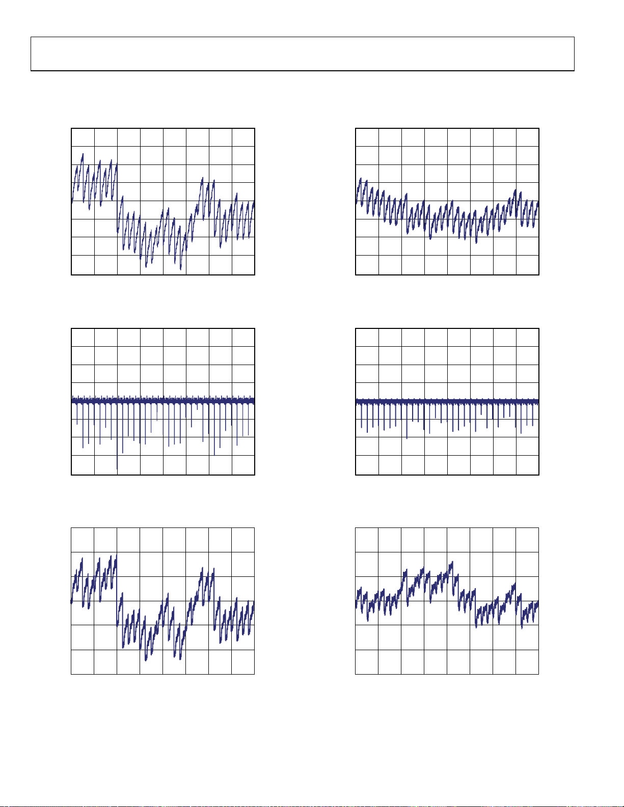
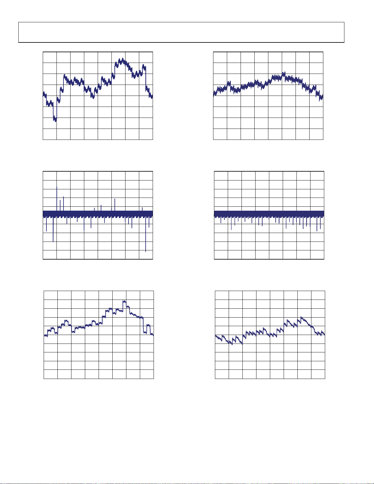
TYPICAL PERFORMANCE CHARACTERISTICS
AVDD, DVDD, DVDDIO, CVDD = 1.8 V, I
2.0
= 8 mA, maximum sample rate (125 MSPS), unless otherwise noted.
xOUTFS
2.0
1.5
1.0
0.5
0
–0.5
–1.0
PRECALIBRATI ON INL (LS B)
–1.5
–2.0
0 2048 4096 6144 8192 10,240 12,288 14, 336 16,384
CODE
Figure 6. AD9117 Precalibration INL at 1.8 V, 8 mA (DVDD = 1.8 V)
2.0
1.5
1.0
0.5
0
–0.5
–1.0
PRECALIBRATIO N DNL (LSB)
–1.5
1.5
1.0
0.5
0
–0.5
–1.0
POSTCALIBRATION INL (LSB)
–1.5
–2.0
0 2048 4096 6144 8192 10,240 12,288 14,336 16,384
07466-006
CODE
07466-009
Figure 9. AD9117 Postcalibration INL at 1.8 V, 8 mA (DVDD = 1.8 V)
2.0
1.5
1.0
0.5
0
–0.5
–1.0
POSTCALI BRATION DNL (L SB)
–1.5
–2.0
0 2048 4096 6144 8192 10,240 12,288 14, 336 16,384
CODE
Figure 7. AD9117 Precalibration DNL at 1.8 V, 8 mA (DVDD = 1.8 V)
1.5
1.0
0.5
0
–0.5
PRECALIBRATIO N INL (LSB)
–1.0
–1.5
0 2048 4096 6144 8192 10,240 12,288 14,336 16,384
CODE
07466-007
7466-008
–2.0
0 2048 4096 6144 8192 10,240 12,288 14,336 16,384
CODE
Figure 10. AD9117 Postcalibration DNL at 1.8 V, 8 mA (DVDD = 1.8 V)
1.5
1.0
0.5
0
–0.5
POSTCALI BRATION INL ( LSB)
–1.0
–1.5
0 2048 4096 6144 8192 10,240 12,288 14,336 16,384
CODE
Figure 8. AD9117 Precalibration INL at 3.3 V, 20 mA (DVDD = 1.8 V) Figure 11. AD9117 Postcalibration INL at 3.3 V, 20 mA (DVDD = 1.8 V)
Rev. A | Page 18 of 80
07466-010
7466-011
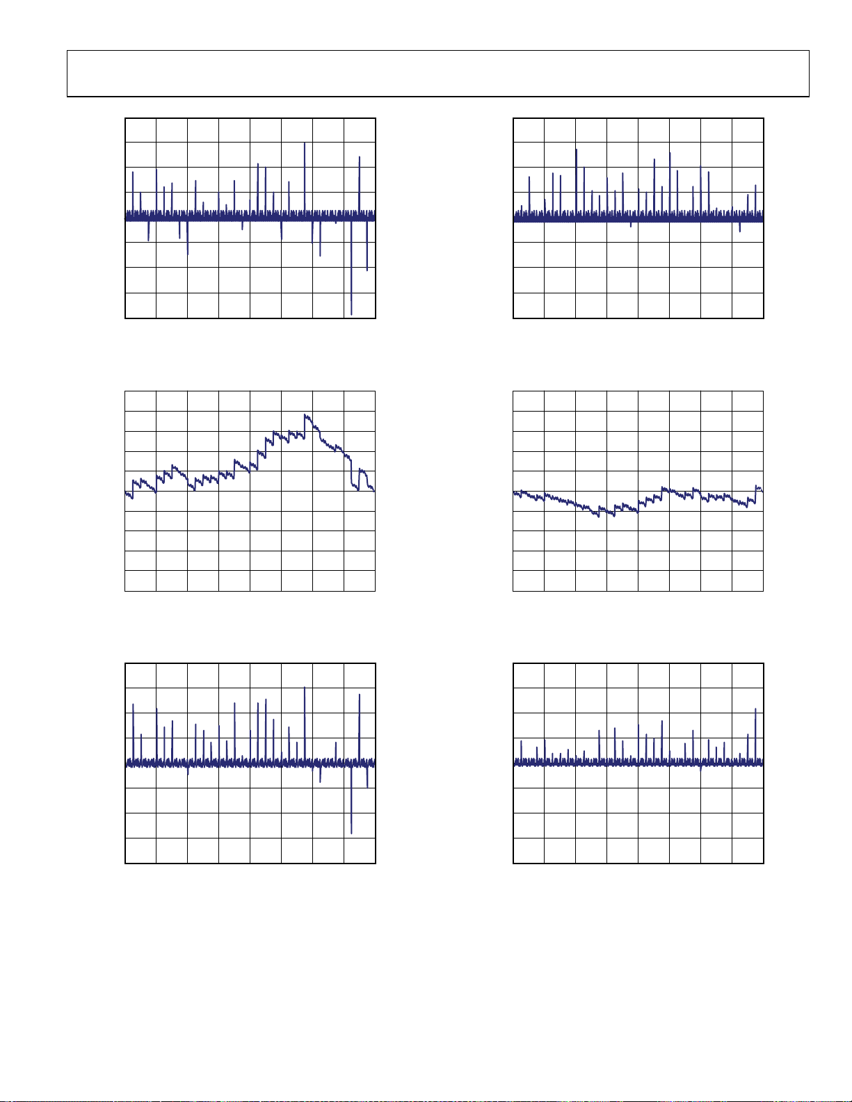
AD9114/AD9115/AD9116/AD9117
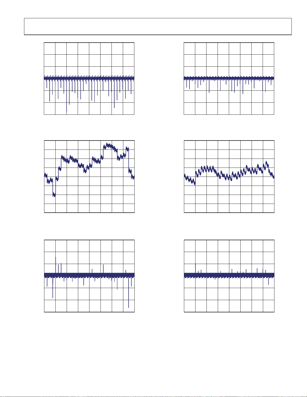
1.5
1.5
1.0
0.5
0
–0.5
PRECALIBRATI ON DNL (LSB)
–1.0
–1.5
0 2048 4096 6144 8192 10,240 12,288 14,336 16,384
CODE
Figure 12. AD9117 Precalibration DNL at 3.3 V, 20 mA
0.8
0.6
0.4
0.2
0
–0.2
–0.4
PRECALIBRATIO N INL (LSB)
–0.6
1.0
0.5
0
–0.5
POSTCALI BRATION DNL (L SB)
–1.0
–1.5
7466-012
0 2048 4096 6144 8192 10,240 12,288 14,336 16,384
CODE
7466-015
Figure 15. AD9117 Postcalibration DNL at 3.3 V, 20 mA
0.8
0.6
0.4
0.2
0
–0.2
–0.4
POSTCALI BRATION INL (LSB)
–0.6
–0.8
0 512 1024 1536 2048 2560 3072 3584 4096
CODE
Figure 13. AD9116 Precalibration INL at 1.8 V, 8 mA
0.6
0.4
0.2
0
–0.2
PRECALIBRATI ON DNL (LSB)
–0.4
–0.6
0 512 1024 1536 2048 2560 3072 3584 4096
CODE
Figure 14. AD9116 Precalibration DNL at 1.8 V, 8 mA
–0.8
7466-013
0 512 1024 1536 2048 2560 3072 3584 4096
CODE
7466-016
Figure 16. AD9116 Postcalibration INL at 1.8 V, 8 mA
0.6
0.4
0.2
0
–0.2
POSTCALI BRATION DNL (L SB)
–0.4
–0.6
7466-014
0 512 1024 1536 2048 2560 3072 3584 4096
CODE
7466-017
Figure 17. AD9116 Postcalibration DNL at 1.8 V, 8 mA
Rev. A | Page 19 of 80
AD9114/AD9115/AD9116/AD9117
0.8
0.8
0.6
0.4
0.2
0
–0.2
–0.4
PRECALIBRATIO N INL (LSB)
–0.6
–0.8
0 512 1024 1536 2048 2560 3072 3584 4096
CODE
Figure 18. AD9116 Precalibration INL at 3.3 V, 20 mA
0.5
0.4
0.3
0.2
0.1
0
–0.1
–0.2
PRECALIBRATIO N DNL (LSB)
–0.3
–0.4
–0.5
0 512 1024 1536 2048 2560 3072 3584 4096
CODE
Figure 19. AD9116 Precalibration DNL at 3.3 V, 20 mA
0.25
0.20
0.15
0.10
0.05
0
–0.05
–0.10
PRECALIBRATION INL (LSB)
–0.15
–0.20
–0.25
0 128 256 384 512 640 768 896 1024
CODE
Figure 20. AD9115 Precalibration INL at 1.8 V, 8 mA
0.6
0.4
0.2
0
–0.2
–0.4
POSTCALI BRATION INL (LSB)
–0.6
–0.8
7466-018
0 512 1024 1536 2048 2560 3072 3584 4096
CODE
7466-021
Figure 21. AD9116 Postcalibration INL at 3.3 V, 20 mA
0.5
0.4
0.3
0.2
0.1
0
–0.1
–0.2
–0.3
POSTCALI BRATION DNL (L SB)
–0.4
–0.5
7466-019
0 512 1024 1536 2048 2560 3072 3584 4096
CODE
07466-022
Figure 22. AD9116 Postcalibration DNL at 3.3 V, 20 mA
0.25
0.20
0.15
0.10
0.05
0
–0.05
–0.10
POSTCALI BRATION INL (LSB)
–0.15
–0.20
–0.25
7466-020
0 128 256 384 512 640 768 896 1024
CODE
07466-023
Figure 23. AD9115 Postcalibration INL at 1.8 V, 8 mA
Rev. A | Page 20 of 80
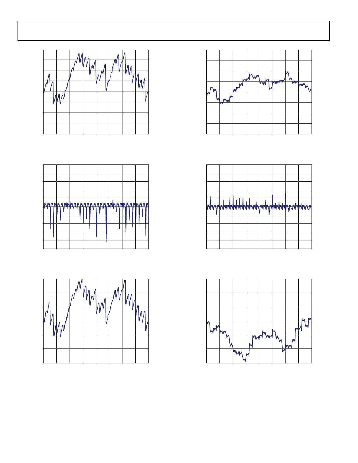
AD9114/AD9115/AD9116/AD9117
0.08
0.08
0.06
0.04
0.02
0
–0.02
–0.04
PRECALIBRATI ON DNL (LSB)
–0.06
–0.08
0 128 256 384 512 640 768 896 1024
CODE
Figure 24. AD9115 Precalibration DNL at 1.8 V, 8 mA
0.25
0.20
0.15
0.10
0.05
0
–0.05
–0.10
PRECALIBRATION INL (LSB)
–0.15
–0.20
–0.25
0 128 256 384 512 640 768 896 1024
CODE
Figure 25. AD9115 Precalibration INL at 3.3 V, 20 mA
0.08
0.06
0.04
0.02
0
–0.02
–0.04
POSTCALI BRATION DNL (L SB)
–0.06
–0.08
0 128 256 384 512 640 768 896 1024
07466-024
CODE
07466-027
Figure 27. AD9115 Postcalibration DNL at 1.8 V, 8 mA
0.25
0.20
0.15
0.10
0.05
0
–0.05
–0.10
POSTCALI BRATION INL (LSB)
–0.15
–0.20
–0.25
7466-025
0 128 256 384 512 640 768 896 1024
CODE
7466-028
Figure 28. AD9115 Postcalibration INL at 3.3 V, 20 mA
0.08
0.06
0.04
0.02
0
–0.02
–0.04
PRECALIBRATI ON DNL (LSB)
–0.06
–0.08
0 128 256 384 512 640 768 896 1024
CODE
Figure 26. AD9115 Precalibration DNL at 3.3 V, 20 mA
07466-026
Rev. A | Page 21 of 80
0.06
0.04
0.02
0
–0.02
–0.04
POSTCALI BRATION DNL (L SB)
–0.06
–0.08
0 128 256 384 512 640 768 896 1024
CODE
Figure 29. AD9115 Postcalibration DNL at 3.3 V, 20 mA
07466-029
AD9114/AD9115/AD9116/AD9117
0.035
0.035
0.025
0.015
0.005
0
–0.005
–0.015
PRECALIBRATI ON INL (LSB)
–0.025
–0.035
0 32 64 96 128 160 192 224 256
CODE
Figure 30. AD9114 Precalibration INL at 1.8 V, 8 mA
0.025
0.020
0.015
0.010
0.005
0
–0.005
–0.010
PRECALIBRATIO N DNL (LSB)
–0.015
–0.020
–0.025
0 32 64 96 128 160 192 224 256
CODE
Figure 31. AD9114 Precalibration DNL at 1.8 V, 8 mA
0.03
0.025
0.015
0.005
0
–0.005
–0.015
POSTCALIBRATION INL (LSB)
–0.025
–0.035
0 32 64 96 128 160 192 224 256
07466-030
CODE
07466-033
Figure 33. AD9114 Postcalibration INL at 1.8 V, 8 mA
0.025
0.020
0.015
0.010
0.005
0
–0.005
–0.010
–0.015
POSTCALI BRATION DNL (L SB)
–0.020
–0.025
0 32 64 96 128 160 192 224 256
07466-031
CODE
07466-034
Figure 34. AD9114 Postcalibration DNL at 1.8 V, 8 mA
0.03
0.02
0.01
0
–0.01
PRECALIBRATIO N INL (LSB)
–0.02
–0.03
0 32 64 96 128 160 192 224 256
CODE
Figure 32. AD9114 Precalibration INL at 3.3 V, 20 mA
07466-032
Rev. A | Page 22 of 80
0.02
0.01
0
–0.01
POSTCALI BRATION INL (LSB)
–0.02
–0.03
0 32 64 96 128 160 192 224 256
CODE
Figure 35. AD9114 Postcalibration INL at 3.3 V, 20 mA
07466-035
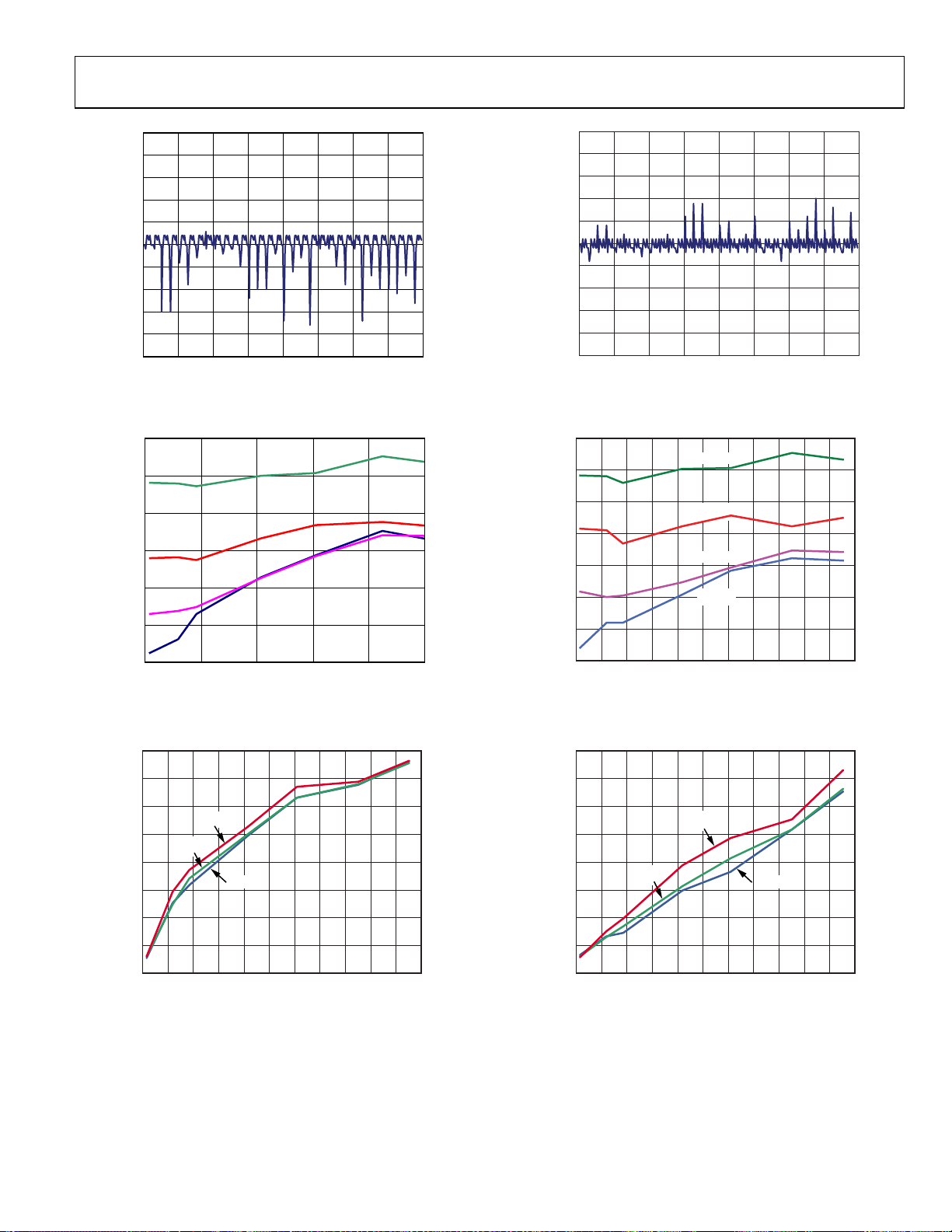
AD9114/AD9115/AD9116/AD9117
–
–
–
–
0.025
0.020
0.015
0.010
0.005
0
–0.005
–0.010
PRECALIBRATIO N DNL (LSB)
–0.015
–0.020
–0.025
0 32 64 96 128 160 192 224 256
CODE
Figure 36. AD9114 Precalibration DNL at 3.3 V, 20 mA
124
–130
AD9114
–136
–142
NSD (dBc)
AD9115
–148
AD9116
–154
AD9117
–160
0 102030405
Figure 37. NSD at 8 mA vs. f
f
(MHz)
OUT
, 1.8 V
OUT
136
07466-036
0
07466-137
0.025
0.020
0.015
0.010
0.005
0
–0.005
–0.010
–0.015
POSTCALI BRATION DNL (LSB)
–0.020
–0.025
0326496128
160 192 224 256
CODE
Figure 39. AD9114 Postcalibration DNL at 3.3 V, 20 mA
124
–130
–136
–142
–148
NSD (dBc)
–154
–160
–166
0 1020305 15253540455055
Figure 40. NSD at 20 mA vs. f
AD9114
AD9115
AD9116
AD9117
f
OUT
(MHz)
OUT
, 3.3 V
136
07466-039
07466-200
–139
–142
–145
–148
–151
NSD (dBm/Hz)
–154
–157
–160
0 1020305 15253540455055
Figure 38. AD9117 NSD at Three Temperatures 8 mA vs. f
+25°C
+85°C
–40°C
f
OUT
(MHz)
OUT
, 1.8 V
07466-201
–139
–142
–145
–148
–151
NSD (dBm/Hz)
–154
–157
–160
0 1020305 15253540455055
+25°C
Figure 41. AD9117 NSD at Three Temperatures 8 mA vs. f
+85°C
f
OUT
–40°C
(MHz)
OUT
, 3.3 V
07466-202
Rev. A | Page 23 of 80
AD9114/AD9115/AD9116/AD9117
–
–
130
130
–136
–142
–148
NSD (dBc)
–154
–160
–166
0 5 10 15 20 25 30 35 40 45 50 55
f
OUT
1.8V, 4mA
1.8V, 8mA
(MHz)
Figure 42. AD9117 NSD at Two Output Currents vs. f
0
–10
–20
–30
–40
–50
(dBm)
–60
–70
–80
–90
–100
START 1MHz 1.5MHz/DIV STOP 16MHz
OUT
, 1.8 V
–136
–142
–148
NSD (dBc)
07466-142
3.3V, 4mA
3.3V, 8mA
–154
–160
3.3V, 20mA
–166
0 5 10 15 20 25 30 35 40 45 50 55
f
OUT
(MHz )
Figure 45. AD9117 NSD at Three Output Currents vs. f
OUT
07466-145
, 3.3 V
0
–10
–20
–30
–40
–50
(dBm)
–60
–70
–80
–90
–100
07466-090
START 1MHz 1.5MHz/DIV STOP 16MHz
07466-091
Figure 43. AD9117 Two Tone Spectrum at 1.8 V
90
AD9117
80
70
IMD (dBc)
60
50
5 10152025303540 4550
AD9116
AD9115
AD9114
f
(MHz)
OUT
Figure 44. All IMD 8 mA vs. f
OUT
, 1.8 V
7466-144
Rev. A | Page 24 of 80
Figure 46. AD9117 Two Tone Spectrum at 3.3 V
96
90
84
78
72
IMD (dBc)
66
60
54
5 101520253035404550
AD9117
AD9116
AD9115
AD9114
f
(MHz)
OUT
Figure 47. All IMD 20 mA vs. f
OUT
, 3.3 V
7466-147

AD9114/AD9115/AD9116/AD9117
84
78
72
66
IMD (dBc)
60
54
48
5 101520253035404550
f
OUT
–40°C
+25°C
+85°C
(MHz)
Figure 48. AD9117 IMD at Three Temperatures 8 mA vs. f
90
85
80
75
70
65
IMD (dBc)
60
55
50
45
5 101520253035404550
f
OUT
–6dB
–3dB
0dB
(MHz)
Figure 49. AD9117 IMD at Three Digital Signal Levels vs. f
86
OUT
OUT
, 1.8 V
, 1.8 V
07466-195
07466-092
90
87
84
81
78
75
IMD (dBc)
72
69
66
63
5 101520253035404550
f
(MHz)
OUT
–40°C
+85°C
Figure 51. AD9117 IMD at Three Temperatures 20 mA vs. f
90
85
80
–6dB
75
70
IMD (dBc)
65
60
55
5 101520253035404550
f
–3dB
0dB
(MHz)
IN
Figure 52. AD9117 IMD at Three Digital Signal Levels vs. f
92
+25°C
, 3.3 V
OUT
, 3.3 V
OUT
07466-196
07466-093
80
74
68
IMD (dBc)
62
56
50
5 101520253035404550
Figure 50. AD9117 IMD at Two Output Currents vs. f
4mA
8mA
f
OUT
(MHz)
OUT
, 1.8 V
07466-150
Rev. A | Page 25 of 80
86
80
74
IMD (dBc)
68
62
56
Figure 53. AD9117 IMD at Three Output Currents vs. f
8mA
4mA
20mA
5 101520253035404550
f
OUT
(MHz)
OUT
, 3.3 V
07466-153

AD9114/AD9115/AD9116/AD9117
0
–10
–20
–30
–40
–50
(dBm)
–60
–70
–80
–90
–100
START 1MHz 1.5MHz/DIV STOP 16MHz
Figure 54. AD9117 Singe Tone Spectrum, 1.8 V
90
80
AD9117
AD9116
AD9115
AD9114
SFDR (dBc)
70
60
50
07466-088
0
–10
–20
–30
–40
–50
(dBm)
–60
–70
–80
–90
–100
START 1MHz 1.5MHz/DIV STOP 16MHz
Figure 57. AD9117 Singe Tone Spectrum, 3.3 V
96
90
84
AD9117
AD9116
AD9115
AD9114
SFDR (dBc)
78
72
66
60
07466-089
40
0 102030405060
Figure 55. SFDR at 8 mA vs. f
f
(MHz)
OUT
, 1.8 V
OUT
90
84
78
72
66
SFDR (dBc)
60
54
48
42
0 5 10 15 20 25 30 35 40 45 50 55 60
Figure 56. AD9117 SFDR at Three Temperatures 8 mA vs. f
–40°C
+25°C
+85°C
f
OUT
(MHz)
OUT
, 1.8 V
54
0 102030405060
07466-155
Figure 58. AD9117 SFDR at 20 mA vs. f
f
OUT
(MHz)
OUT
, 3.3 V
07466-158
98
92
86
80
74
SFDR (dBc)
68
62
56
0 5 10 15 20 25 30 35 40 45 50 55 60
07466-156
Figure 59. AD9117 SFDR at Three Temperatures 8 mA vs. f
–40°C
+25°C
+85°C
f
OUT
(MHz)
OUT
, 3.3 V
07466-159
Rev. A | Page 26 of 80

AD9114/AD9115/AD9116/AD9117
V
V
98
98
90
82
74
66
SFDR (dBc)
58
50
42
0 5 10 15 20 25 30 35 40 45 50 55 60
f
(MHz)
OUT
Figure 60. AD9117 SFDR at Three Digital Signal Levels vs. f
96
90
84
78
72
66
SFDR (dBc)
60
54
48
42
0 10203040506
4mA
8mA
f
(MHz)
OUT
–6dB
–3dB
0dB
OUT
, 1.8 V
0
90
82
74
SFDR (dBc)
66
58
50
0 5 10 15 20 25 30 35 40 45 50 55 60
07466-094
f
OUT
(MHz)
Figure 63. AD9117 SFDR at Three Digital Signal Levels vs. f
–6dB
–3dB
0dB
OUT
., 3.3 V
07466-095
96
90
84
78
72
66
SFDR (dBc)
60
54
48
07466-161
42
0 102030405060
4mA
8mA
20mA
f
OUT
(MHz)
07466-164
Figure 61. AD9117 SFDR at Two Currents vs. f
AC COUPLED: UNSPECI FIED
BELOW 20MHz
10dB/DI
INPUT ATT
8.00dB
STEP
2dB
CENTER 22.90MHz
RES BW 30kHz SWEEP 126ms ( 601pts)
TOTAL CARRIER POWER –12 .17dBm/7.87420M Hz
REF CARRIER PO WER –12.17d Bm/4.03420MHz
RCC FILTER: OFF F ILTER AL PHA 0.22
1. –12.17dBm 5. 000MHz 3.840MHz –77.40 –89.56 –78. 68 –90.84
2. –80.85dBm 10.00MHz 3.840MHz –78.90 –91.06 –78.27 –90.43
15.00MHz 3. 840MHz –78.02 –90. 18 –70.99 –83.15
OFFSET
FREQ
VBW 300kHz
INTEG
BW
LOWER UPPER
dBc dBm dBc
, 1.8 V
OUT
SPAN 38.84MHz
dBm
Figure 62. AD9117 ACLR One-Carrier, 1.8 V
Figure 64. AD9117 SFDR at Three Currents vs. f
AC COUPLED: UNSPECI FIED
BELOW 20MHz
10dB/DI
INPUT ATT
8.00dB
STEP
2dB
CENTER 22.90MHz
RES BW 30kHz SWEEP 126ms (601pts)
TOTAL CARRIER POWER –12 .17dBm/7.87420M Hz
REF CARRIER PO WER –12.17d Bm/4.03420MHz
RCC FILTER: OFF F ILTER AL PHA 0.22
1. –12.17dBm 5. 000MHz 3.840MHz –77.40 –89.56 –78. 68 –90.84
2. –80.85dBm 10.00MHz 3.840MHz –78.90 –91.06 –78.27 –90.43
07466-162
15.00MHz 3. 840MHz –78.02 –90. 18 –70.99 –83.15
OFFSET
FREQ
VBW 300kHz
INTEG
BW
LOWER UPPER
dBc dBm dBc
Figure 65. AD9117 ACLR One-Carrier, 3.3 V
, 3.3V
OUT
SPAN 38.84MHz
07466-165
Rev. A | Page 27 of 80

AD9114/AD9115/AD9116/AD9117
–
–
–
–
–
–
60
4mA PRECAL
4mA POST CAL
8mA PRECAL
8mA POST CAL
–66
–66
60
4mA PRECAL
4mA POST CAL
8mA PRECAL
8mA POST CAL
16mA PRECAL
16mA POSTCAL
ACLR (dBc)
–72
–78
15 20 25 30 35 40 45
f
(MHz)
OUT
Figure 66. AD9117 One-Carrier W-CDMA First ACLR vs. f
62
4mA PRECAL
4mA POST CAL
8mA PRECAL
8mA POST CAL
–68
ACLR (dBc)
–74
–80
15 20 25 30 35 40 45
f
(MHz)
OUT
Figure 67. AD9117 One-Carrier W-CDMA Second ACLR vs. f
62
4mA PRECAL
4mA POSTCAL
8mA PRECAL
8mA POSTCAL
–68
OUT
, 1.8 V
OUT
, 1.8 V
ACLR (dBc)
–72
–78
07466-166
15 20 25 30 35 40 45
f
(MHz)
OUT
Figure 69. AD9117 One-Carrier W-CDMA First ACLR vs. f
OUT
07466-169
, 3.3 V
62
–68
ACLR (dBc)
–74
–80
07466-167
15 25 35 45
Figure 70. AD9117 One-Carrier W-CDMA Second ACLR vs. f
f
(MHz)
OUT
4mA PRECAL
4mA POSTCAL
8mA PRECAL
8mA POSTCAL
16mA PRECAL
16mA POSTCAL
OUT
07466-170
, 3.3 V
62
4mA PRECAL
4mA POSTCAL
8mA PRECAL
8mA POSTCAL
–68
16mA PRECAL
16mA POST CAL
ACLR (dBc)
–74
–80
20 25 30 35 40 45
f
(MHz)
OUT
Figure 68. AD9117 One-Carrier W-CDMA Third ACLR vs. f
OUT
07466-168
, 1.8 V
ACLR (dBc)
–74
–80
20 25 30 35 40 45
f
(MHz)
OUT
Figure 71. AD9117 One-Carrier W-CDMA Third ACLR vs. f
OUT
07466-171
, 3.3 V
Rev. A | Page 28 of 80

AD9114/AD9115/AD9116/AD9117
V
–
–
V
–
–
AC COUPLED: UNSPECI FIED
BELOW 20MHz
10dB/DI
INPUT ATT
8.00dB
STEP
2dB
CENTER 22.90MHz
RES BW 30kHz SWEEP 126ms (601pts)
TOTAL CARRIER POWER –15 .23dBm/7.87420M Hz
REF CARRIER PO WER –18.09d Bm/4.03420MHz
RCC FILTER: OFF F ILTER AL PHA 0.22
1. –18.09dBm 5. 000MHz 3.840MHz –72.11 –90.24 –71. 97 –90.09
2. –18.40dBm 10.00MHz 3.840MHz –72.98 –91.10 –72.55 –90.68
15.00MHz 3. 840MHz –69.93 –88. 05 –72.30 –90.42
OFFSET
FREQ
VBW 300kHz
INTEG
BW
dBc dBm dBc
SPAN 38.84MHz
LOWER UPPER
dBm
Figure 72. AD9117 ACLR Two-Carrier, 1.8 V
50
4mA PRECAL
4mA POSTCAL
–56
8mA PRECAL
8mA POSTCAL
AC COUPLED: UNSPECI FIED
BELOW 20MHz
10dB/DI
1. –18.09dBm 5. 000MHz 3.840MHz –72.11 –90.24 –71. 97 –90.09
2. –18.40dBm 10.00MHz 3.840MHz –72.98 –91.10 –72.55 –90.68
07466-172
15.00MHz 3. 840MHz –69.93 –88. 05 –72.30 –90.42
INPUT ATT
8.00dB
STEP
2dB
CENTER 22.90MHz
RES BW 30kHz SWEEP 126ms (601pts)
TOTAL CARRIER POWER –15 .23dBm/7.87420M Hz
REF CARRIER PO WER –18.09d Bm/4.03420MHz
RCC FILTER: OFF F ILTER AL PHA 0.22
OFFSET
FREQ
VBW 300kHz
INTEG
BW
dBc dBm dBc
SPAN 38.84MHz
LOWER UPPER
dBm
07466-175
Figure 75. AD9117 ACLR Two-Carrier, 3.3 V
50
4mA PRECAL
4mA POSTCAL
8mA PRECAL
–56
8mA POSTCAL
16mA PRECAL
16mA POSTCAL
–62
ACLR (dBc)
–68
–74
15 20 25 30 35 40
Figure 73. AD9117 Two- Carrier W-CDMA First ACLR vs. f
f
OUT
(MHz)
OUT
50
4mA PRECAL
4mA POSTCAL
–56
–62
ACLR (dBc)
–68
–74
8mA PRECAL
8mA POSTCAL
15 20 25 30 35 40
f
OUT
(MHz)
Figure 74. AD9117 Two-Carrier W-CDMA Second ACLR vs. f
, 1.8 V
, 1.8 V
OUT
–62
ACLR (dBc)
–68
–74
15 20 25 30 35 40
07466-173
Figure 76. AD9117 Two- Carrier W-CDMA First ACLR vs. f
f
OUT
(MHz)
OUT
, 3.3 V
07466-176
50
4mA PRECAL
4mA POSTCAL
8mA PRECAL
–56
–62
ACLR (dBc)
–68
–74
07466-174
Figure 77. AD9117 Two-Carrier W-CDMA Second ACLR vs. f
8mA POSTCAL
16mA PRECAL
16mA POSTCAL
15 20 25 30 35 40
f
OUT
(MHz)
OUT
, 3.3 V
07466-177
Rev. A | Page 29 of 80

AD9114/AD9115/AD9116/AD9117
–
–
R
m
–56
50
4mA PRECAL
4mA POSTCAL
8mA PRECAL
8mA POSTCAL
–56
50
4mA PRECAL
4mA POSTCAL
8mA PRECAL
8mA POSTCAL
16mA PRECAL
16mA POSTCAL
–62
ACLR (dBc)
–68
–74
20 25 30 35 40
f
OUT
(MHz)
Figure 78. AD9117 Two-Carrier W-CDMA Third ACLR vs. f
0.4
0.3
0.2
0.1
0
–0.1
–0.2
AUXDAC DNL (LSB)
–0.3
–0.4
–0.5
128 256 384 512 640 768 896 1024
0
CODE
OUT
, 1.8 V
–62
ACLR (dBc)
–68
–74
20 25 30 35 40
7466-178
Figure 81. AD9117 Two-Carrier W-CDMA Third ACLR vs. f
f
OUT
(MHz)
OUT
, 3.3 V
7466-181
1.0
0.8
0.6
0.4
0.2
0
–0.2
AUXDAC INL (LSB)
–0.4
–0.6
–0.8
–1.0
0
7466-047
128 256 384 512 640 768 896 1024
CODE
7466-044
Figure 79. AD9114/AD9115/AD9116/AD9117 AUXDAC DNL
40
30
20
SUPPLY CURRENT (mA)
10
TOTAL CURRENT @ 8mA OUT
AVDD @ 8mA OUT
TOTAL CURRENT @ 4mA OUT
AVDD @ 4mA OUT
DVDD
0
0 20 40 60 80 100 120 140
f
DAC
CVDD
(MHz)
Figure 80. AD9114/AD9115/AD9116/AD9117 Supply Current vs. f
07466-048
, 1.8 V
DAC
Rev. A | Page 30 of 80
Figure 82. AD9114/AD9115/AD9116/AD9117 AUXDAC INL
80
70
TOTAL CURRENT @ 20mA OUT
60
50
A)
40
ENT (
30
CUR
20
10
AVDD @ 20mA OUT
TOTAL CURRENT @ 8mA OUT
TOTAL CURRENT @ 4mA OUT
AVDD @ 4mA OUT
DVDD
0
0 20406080100120140
f
(MHz )
DAC
AVDD @ 8mA OUT
CVDD
Figure 83. AD9114/AD9115/AD9116/AD9117Supply Current vs. f
DAC
7466-183
, 3.3 V

AD9114/AD9115/AD9116/AD9117
TERMINOLOGY
Linearity Error or Integral Nonlinearity (INL)
Linearity error is defined as the maximum deviation of the
actual analog output from the ideal output, determined by
a straight line drawn from zero scale to full scale.
Differential Nonlinearity (DNL)
DNL is the measure of the variation in analog value, normalized
to full scale, associated with a 1 LSB change in digital input code.
Monotonicity
A DAC is monotonic if the output either increases or remains
constant as the digital input increases.
Offset Error
Offset error is the deviation of the output current from the ideal
of zero. For I
are all 0. For I
, the 0 mA output is expected when the inputs
OUTP
, the 0 mA output is expected when all inputs
OUTN
are set to 1.
Gain Error
Gain error is the difference between the actual and the ideal
output span. The actual span is determined by the difference
between the output when all inputs are set to 1 and the output
when all inputs are set to 0.
Output Compliance Range
The output compliance range is the range of allowable voltage at
the output of a current output DAC. Operation beyond the
maximum compliance limits can cause either output stage
saturation or breakdown, resulting in nonlinear performance.
Temp er a tu r e D ri ft
Temperature drift is specified as the maximum change from
the ambient value (25°C) to the value at either T
MIN
or T
MAX
.
For offset and gain drift, the drift is reported in ppm of fullscale range per degree Celsius (ppm FSR/°C). For reference
drift, the drift is reported in parts per million per degree
Celsius (ppm/°C).
Power Supply Rejection
Power supply rejection is the maximum change in the full-scale
output as the supplies are varied from minimum to maximum
specified voltages.
Settling Time
Settling time is the time required for the output to reach and
remain within a specified error band around its final value,
measured from the start of the output transition.
Spurious Free Dynamic Range (SFDR)
SFDR is the difference, in decibels (dB), between the peak
amplitude of the output signal and the peak spurious signal
between dc and the frequency equal to half the input data rate.
Total Harmonic Distortion (THD)
THD is the ratio of the rms sum of the first six harmonic
components to the rms value of the measured fundamental.
It is expressed as a percentage (%) or in decibels (dB).
Signal-to-Noise Ratio (SNR)
SNR is the ratio of the rms value of the measured output signal
to the rms sum of all other spectral components below the Nyquist
frequency, excluding the first six harmonics and dc. The value
for SNR is expressed in decibels (dB).
Adjacent Channel Leakage Ratio (ACLR)
ACLR is the ratio in decibels relative to the carrier (dBc)
between the measured power within a channel relative to
its adjacent channel.
Complex Image Rejection
In a traditional two-part upconversion, two images are created
around the second IF frequency. These images have the effect
of wasting transmitter power and system bandwidth. By placing
the real part of a second complex modulator in series with the
first complex modulator, either the upper or lower frequency
image near the second IF can be rejected.
Rev. A | Page 31 of 80

AD9114/AD9115/AD9116/AD9117
THEORY OF OPERATION
DB12
DB13 (MSB)
CS/PW RDN
SDIO/FORMAT
SCLK/CLKMD
RESET/PINMD
REFIO
FSADJQ/AUXQ
FSADJI/AUXI
CMLI
1V
DB11
DB10
DB9
DB8
DVDDIO
DVSS
DVDD
DB7
DB6
DB5
1.8V
LDO
DB4
DB3
SPI
INTERFACE
1 INTO 2
INTERLEAVED
DATA
INTERFACE
DB2
DB1
(LSB) DB0
I
REF
100µA
DCLKIO
QR
BAND
GAP
I DATA
Q DATA
SET
2kΩ
10kΩ
Figure 84. Simplified Block Diagram
Figure 84 shows a simplified block diagram of the AD9114/
AD9115/AD9116/AD9117 that consists of two DACs, digital
control logic, and a full-scale output current control. Each DAC
contains a PMOS current source array capable of providing a
maximum of 20 mA. The arrays are divided into 31 equal currents
that make up the five most significant bits (MSBs). The next four
bits, or middle bits, consist of 15 equal current sources whose
value is 1/16 of an MSB current source. The remaining LSBs are
binary weighted fractions of the current sources of the middle
bits. Implementing the middle and lower bits with current sources,
instead of an R-2R ladder, enhances its dynamic performance for
multitone or low amplitude signals and helps maintain the high
output impedance of the main DACs (that is, >200 M).
The current sources are switched to one or the other of the two
output nodes (I
OUTP
or I
) via PMOS differential current switches.
OUTN
The switches are based on the architecture that was pioneered in
the AD976x family, with further refinements to reduce distortion
contributed by the switching transient. This switch architecture also
reduces various timing errors and provides matching complementary
drive signals to the inputs of the differential current switches.
The analog and digital I/O sections of the AD9114/AD9115/
AD9116/AD9117 have separate power supply inputs (AVDD and
DVDDIO) that can operate independently over a 1.8 V to 3.3 V
range. The core digital section requires 1.8 V. An optional on-chip
LDO is provided for DVDDIO supplies greater than 1.8 V, or the
AD9117
IR
SET
CLOCK
DIST
CVDD
CLKIN
2kΩ
AUX1DAC
AUX2DAC
CVSS
I DAC
Q DAC
IR
60Ω TO
260Ω
QR
60Ω TO
260Ω
CM
CM
CMLQ
62.5Ω
62.5Ω
62.5Ω
62.5Ω
RLIN
IOUTN
IOUTP
RLIP
AVDD
AVSS
RLQP
QOUTP
QOUTN
RLQN
07466-050
1.8 V can be supplied directly through DVDD. A 1.0 µF bypass
capacitor at DVDD (Pin 7) is required when using the LDO.
The core is capable of operating at a rate of up to 125 MSPS. It
consists of edge-triggered latches and the segment decoding logic
circuitry. The analog section includes PMOS current sources,
associated differential switches, a 1.0 V band gap voltage
reference, and a reference control amplifier.
Each DAC full-scale output current is regulated by the reference
control amplifier and can be set from 4 mA to 20 mA via an
external resistor, xR
, connected to its full-scale adjust pin
SET
(FSADJx).
The external resistor, in combination with both the reference control
amplifier and voltage reference, V
, sets the reference current, I
REFIO
which is replicated to the segmented current sources with the proper
scaling factor. The full-scale current, I
Optional on-chip xR
resistors are provided that can be
SET
xOUTFS
, is 32 × I
xREF
.
programmed between a nominal value of 1.6 k to 8 k (4 mA
to 20 mA I
, respectively).
xOUTFS
The AD9114/AD9115/AD9116/AD9117 provide the option of
setting the output common mode to a value other than AGND via
the output common-mode pin (CMLI and CMLQ). This facilitates
directly interfacing the output of the AD9114/AD9115/AD9116/
AD9117 to components that require common-mode levels greater
than 0 V.
xREF
,
Rev. A | Page 32 of 80

AD9114/AD9115/AD9116/AD9117
SERIAL PERIPHERAL INTERFACE (SPI)
The serial port of the AD9114/AD9115/AD9116/AD9117 is a
flexible, synchronous serial communications port that allows easy
interfacing to many industry-standard microcontrollers and microprocessors. The serial I/O is compatible with most synchronous
transfer formats, including both the Motorola SPI and Intel® SSR
protocols. The interface allows read/write access to all registers
that configure the AD9114/AD9115/AD9116/AD9117. Single or
multiple byte transfers are supported, as well as MSB first or
LSB first transfer formats. The serial interface port of the AD9114/
AD9115/AD9116/AD9117 is configured as a single I/O pin on
the SDIO pin.
GENERAL OPERATION OF THE SERIAL INTERFACE
There are two phases to a communication cycle on the AD9114/
AD9115/AD9116/AD9117. Phase 1 is the instruction cycle, which
is the writing of an instruction byte into the AD9114/AD9115/
AD9116/AD9117, coinciding with the first eight SCLK rising
edges. In Phase 2, the instruction byte provides the serial port
controller of the AD9114/AD9115/AD9116/AD9117 with information regarding the data transfer cycle. The Phase 1 instruction
byte defines whether the upcoming data transfer is a read or write,
the number of bytes in the data transfer, and the starting register
address for the first byte of the data transfer. The first eight SCLK
rising edges of each communication cycle are used to write the
instruction byte into the AD9114/AD9115/AD9116/AD9117.
A Logic 1 on Pin 35 (RESET/PINMD), followed by a Logic 0,
resets the SPI port timing to the initial state of the instruction
cycle. This is true regardless of the present state of the internal
registers or the other signal levels present at the inputs to the
SPI port. If the SPI port is in the midst of an instruction cycle
or a data transfer cycle, none of the present data is written.
The remaining SCLK edges are for Phase 2 of the communication
cycle. Phase 2 is the actual data transfer between the AD9114/
AD9115/AD9116/AD9117 and the system controller. Phase 2
of the communication cycle is a transfer of one, two, three, or
four data bytes, as determined by the instruction byte. Using a
multibyte transfer is the preferred method. Single byte
data transfers are useful to reduce CPU overhead when register
access requires one byte only. Registers change immediately
upon writing to the last bit of each transfer byte.
INSTRUCTION BYTE
The instruction byte contains the information shown in Tab l e 1 1 .
Table 11.
MSB LSB
DB7 DB6 DB5 DB4 DB3 DB2 DB1 DB0
R/W
R/W (Bit 7 of the instruction byte) determines whether a read or a
write data transfer occurs after the instruction byte write. Logic 1
indicates a read operation. Logic 0 indicates a write operation.
N1 and N0 (Bit 6 and Bit 5 of the instruction byte) determine the
number of bytes to be transferred during the data transfer cycle.
The bit decodes are shown in Table 1 2 .
Table 12. Byte Transfer Count
N1 N0 Description
0 0 Transfer 1 byte
0 1 Transfer 2 bytes
1 0 Transfer 3 bytes
1 1 Transfer 4 bytes
A4, A3, A2, A1, and A0 (Bit 4, Bit 3, Bit 2, Bit 1, and Bit 0 of the
instruction byte) determine which register is accessed during the
data transfer portion of the communications cycle. For multibyte transfers, this address is the starting byte address. The
following register addresses are generated internally by the
AD9114/AD9115/AD9116/AD9117 based on the LSBFIRST bit
(Register 0x00, Bit 6).
N1 N0 A4 A3 A2 A1 A0
SERIAL INTERFACE PORT PIN DESCRIPTIONS
SCLK—Serial Clock
The serial clock pin is used to synchronize data to and from the
AD9114/AD9115/AD9116/AD9117 and to run the internal state
machines. The SCLK maximum frequency is 20 MHz. All data
input to the AD9114/AD9115/AD9116/AD9117 is registered on
the rising edge of SCLK. All data is driven out of the AD9114/
AD9115/AD9116/AD9117 on the falling edge of SCLK.
CS
—Chip Select
An active low input starts and gates a communications cycle. It
allows more than one device to be used on the same serial communications lines. The SDIO/FORMAT pin reaches a high impedance
state when this input is high. Chip select should stay low during
the entire communication cycle.
SDIO—Serial Data I/O
The SDIO pin is used as a bidirectional data line to transmit
and receive data.
Rev. A | Page 33 of 80

AD9114/AD9115/AD9116/AD9117
K
K
MSB/LSB TRANSFERS
The serial port of the AD9114/AD9115/AD9116/AD9117 can
support both most significant bit (MSB) first or least significant
bit (LSB) first data formats. This functionality is controlled by the
LSBFIRST bit (Register 0x00, Bit 6). The default is MSB first
(LSBFIRST = 0).
When LSBFIRST = 0 (MSB first), the instruction and data bytes
must be written from the most significant bit to the least significant
bit. Multibyte data transfers in MSB first format start with an
instruction byte that includes the register address of the most
significant data byte. Subsequent data bytes should follow in
order from a high address to a low address. In MSB first mode,
the serial port internal byte address generator decrements for
each data byte of the multibyte communications cycle.
When LSBFIRST = 1 (LSB first), the instruction and data bytes
must be written from the least significant bit to the most significant
bit. Multibyte data transfers in LSB first format start with an
instruction byte that includes the register address of the least
significant data byte followed by multiple data bytes. The serial
port internal byte address generator increments for each byte of
the multibyte communication cycle.
If the MSB first mode is active, the serial port controller data
address of the AD9114/AD9115/AD9116/AD9117 decrements
from the data address written toward 0x00 for multibyte I/O
operations. If the LSB first mode is active, the serial port controller
address increments from the data address written toward 0x1F
for multibyte I/O operations.
SERIAL PORT OPERATION
The serial port configuration of the AD9114/AD9115/AD9116/
AD9117 is controlled by Register 0x00. It is important to note
that the configuration changes immediately upon writing to the
last bit of the register. For multibyte transfers, writing to this
register can occur during the middle of the communications
cycle. Care must be taken to compensate for this new configuration for the remaining bytes of the current communications cycle.
The same considerations apply to setting the software reset bit
(Register 0x00, Bit 5). All registers are set to their default values
except Register 0x00, which remains unchanged.
Use of single-byte transfers or initiating a software reset is
recommended when changing serial port configurations to
prevent unexpected device behavior.
INSTRUCTIO N CYCLE DATA TRANSFER CYCLE
CS
INSTRUCTIO N CYCLE DATA TRANSFER CYCLE
CS
SCLK
SDIO
SDO
R/WN1N0A4A3A2A1A0D7D6ND5
N
D00D10D20D3
0
07466 -290
Figure 86. Serial Register Interface Timing, MSB First Read
INSTRUCTION CYCLE DATA TRANSFER CYCLE
CS
SCL
SDIO
A0 A1 A2 A3 A4 N0 N1 R/W D00D10D2
0
D7ND6ND5ND4
N
7466-289
Figure 87. Serial Register Interface Timing, LSB First Write
INSTRUCTIO N CYCLE DATA TRANSFER CYCLE
CS
SCLK
SDIO
SDO
A0 A1 A2 A3 A4 N0 N1 R /W D10D2
D0
0
D7ND6ND5ND4
N
07466-288
Figure 88. Serial Register Interface Timing, LSB First Read
PIN MODE
The AD9114/AD9115/AD9116/AD9117 can also be operated
without ever writing to the serial port. With RESET/PINMD
(Pin 35) tied high, the SCLK pin becomes CLKMD to provide
for clock mode control (see the Retimer section), the SDIO
pin becomes FORMAT and selects the input data format, and
CS
the
/PWRDN pin serves to power down the device.
Operation is otherwise exactly as defined by the default register
values in Table 1 3; therefore, external resistors at FSADJI and
FSADJQ are needed to set the DAC currents, and both DACs
are active. This is also a convenient quick checkout mode. DAC
currents can be externally adjusted in pin mode by sourcing or
sinking currents at the FSADJI/AUXI and FSADJQ/AUXQ
pins, as desired, with the fixed resistors installed. An op amp
output with appropriate series resistance is one of many
possibilities. This has the same effect as changing the resistor
value. Place at least 10 kΩ resistors in series right at the DAC
to guard against accidental short circuits and noise
modulation. The REFIO pin can be adjusted ±25% in a similar
manner, if desired.
SCL
SDIO
R/WN1N0A4A3A2A1A0D7ND6ND5
N
D00D10D20D3
0
07466-291
Figure 85. Serial Register Interface Timing, MSB First Write
Rev. A | Page 34 of 80

AD9114/AD9115/AD9116/AD9117
SPI REGISTER MAP
Table 13.
Name Addr Default Bit 7 Bit 6 Bit 5 Bit 4 Bit 3 Bit 2 Bit 1 Bit 0
SPI Control 0x00 0x00 Reserved LSBFIRST Reset LNGINS Reserved
Power-Down 0x01 0x40 LDOOFF LDOSTAT PWRDN Q DACOFF I DACOFF QCLKOFF ICLKOFF EXTREF
Data Control 0x02 0x34 TWOS Reserved IFIRST IRISING SIMULBIT DCI_EN DCOSGL DCODBL
I DAC Gain 0x03 0x00 Reserved I DACGAIN[5:0]
IRSET 0x04 0x00 IRSETEN Reserved IRSET[5:0]
IRCML 0x05 0x00 IRCMLEN Reserved IRCML[5:0]
Q DAC Gain 0x06 0x00 Reserved Q DACGAIN[5:0]
QRSET 0x07 0x00 QRSETEN Reserved QRSET[5:0]
QRCML 0x08 0x00 QRCMLEN Reserved QRCML[5:0]
AUXDAC Q 0x09 0x00 QAUXDAC[7:0]
AUX CTLQ 0x0A 0x00 QAUXEN QAUXRNG[1:0] QAUXOFS[2:0] QAUXDAC[9:8]
AUXDAC I 0x0B 0x00 IAUXDAC[7:0]
AUX CTLI 0x0C 0x00 IAUXEN IAUXRNG[1:0] IAUXOFS[2:0] IAUXDAC[9:8]
Reference Resistor 0x0D 0x00 Reserved RREF[5:0]
Cal Control 0x0E 0x00 PRELDQ PRELDI CALSELQ CALSELI CALCLK DIVSEL[2:0]
Cal Memory 0x0F 0x00 CALSTATQ CALSTATI Reserved CALMEMQ[1:0] CALMEMI[1:0]
Memory Address 0x10 0x00 Reserved MEMADDR[5:0]
Memory Data 0x11 0x34 Reserved MEMDATA[5:0]
Memory R/W 0x12 0x00 CALRSTQ CALRSTI CALEN SMEMWR SMEMRD UNCALQ UNCALI
CLKMODE 0x14 0x00 CLKMODEQ[1:0] Searching Reacquire CLKMODEN CLKMODEI[1:0]
Version 0x1F 0x09 Version[7:0]
Rev. A | Page 35 of 80

AD9114/AD9115/AD9116/AD9117
SPI REGISTER DESCRIPTIONS
Reading these registers returns previously written values for all defined register bits, unless otherwise noted.
Table 14.
Register Address Bit Name Description
SPI Control 0x00 6 LSBFIRST 0 (default): MSB first per SPI standard.
1: LSB first per SPI standard.
5 Reset
1: set software reset; write 0 on the next (or any following) cycle to release reset.
4 LNGINS 0 (default): the SPI instruction word uses a 5-bit address.
1: the SPI instruction word uses a 13-bit address.
Power Down 0x01 7 LDOOFF 0 (default): LDO voltage regulator on.
1: powers down the internal voltage reference (external reference required).
Data Control 0x02 7 TWOS 0 (default): Unsigned binary input data format.
1: twos complement input data format.
5 IFIRST 0: pairing of data—Q first of pair on data input pads.
1(default): pairing of data—I first of pair on data input pads (default).
4 IRISING 0: Q data latched on DCLKIO rising edge.
1(default): I data latched on DCLKIO rising edge (default).
3 SIMULBIT 0 (default): allows simultaneous input and output enable on DCLKIO.
1: disallows simultaneous input and output enable on DCLKIO.
2 DCI_EN Controls the use of the DCLKIO pad for the data clock input.
0: data clock input disabled.
1(default): data clock input enabled.
1 DCOSGL Controls the use of the DCLKIO pad for the data clock output.
0 (default): data clock output disabled.
1: data clock output enabled; regular strength driver.
0 DCODBL Controls the use of the DCLKIO pad for the data clock output.
0 (default): DCODBL data clock output disabled.
1: DCODBL data clock output enabled; paralleled with DCOSGL for 2× drive current.
I DAC Gain 0x03 5:0 I DACGAIN[5:0]
1: turns core LDO voltage regulator off.
6 LDOSTAT 0: indicates that the core LDO voltage regulator is off.
1 (default): indicates that the core LDO voltage regulator is on.
5 PWRDN 0 (default): all analog, digital circuitry and SPI logic are powered on.
1: powers down all analog and digital circuitry, except for SPI logic.
4 Q DACOFF 0 (default): turns on Q DAC output current.
1: turns off Q DAC output current.
3 I DACOFF 0 (default): turns on I DAC output current.
1: turns off I DAC output current.
2 QCLKOFF 0 (default): turns on Q DAC clock.
1: turns off Q DAC clock.
1 ICLKOFF 0 (default): turns on I DAC clock.
1: turns off I DAC clock.
0 EXTREF 0 (default): turns on internal voltage reference.
Note that the user must always change the LSB/MSB order in single-byte
instructions to avoid erratic behavior due to bit order errors.
Executes software reset of SPI and controllers, reloads default register values,
except Register 0x00.
DAC I fine gain adjustment; alters the full-scale current, as shown in Figure 99.
Default IDACGAIN = 0x00.
Rev. A | Page 36 of 80

AD9114/AD9115/AD9116/AD9117
Register Address Bit Name Description
IRSET 0x04 7 IRSETEN
0 (default): IR
to the FADJI/AUXI pin. Nominal value for this external resistor is 4 kΩ.
1: enables the on-chip IR
5:0 IRSET[5:0]
Changes the value of the on-chip IR
the DAC in ~0.25 dB steps twos complement (nonlinear), see Figure 98.
000000 (default): IR
011111: IR
100000: IR
111111: IR
IRCML 0x05 7 IRCMLEN
0 (default): IR
connected to CMLI pin. Recommended value for this external resistor is 0 Ω.
1: enables on-chip IR
5:0 IRCML[5:0]
Changes the value of the on-chip IR
common-mode level of the DAC output stage.
000000 (default): IR
100000: IR
111111: IR
Q DAC Gain 0x06 5:0 Q DACGAIN[5:0]
DAC Q fine gain adjustment; alters the full-scale current, as shown in Figure 99.
Default QDACGAIN = 0x00.
QRSET 0x07 7 QRSETEN
0 (default): QR
connected to FADJI/AUXI pin. Nominal value for this external resistor is 4 kΩ.
1: enables on-chip QR
5:0 QRSET[5:0]
Changes the value of the on-chip QR
the DAC in ~0.25 dB steps twos complement (nonlinear).
000000 (default): QR
011111: QR
100000: QR
111111: QR
QRCML 0x08 7 QRCMLEN
0 (default): QR
connected to CMLQ pin. Recommended value for this external resistor is 0 Ω.
1: enables on-chip QR
5:0 QRCML[5:0]
Changes the value of the on-chip QR
common-mode level of the DAC output stage.
000000 (default): QR
100000: QR
111111: QR
AUXDAC Q 0x09 7:0 QAUXDAC[7:0] AUXDAC Q output voltage adjustment word LSBs.
0x3FF: sets AUXDAC Q output to full scale.
0x200: sets AUXDAC Q output to midscale.
0x000 (default): sets AUXDAC Q output to bottom of scale.
AUX CTLQ 0x0A 7 QAUXEN 0 (default): AUXDAC Q output disabled.
1: enables AUXDAC Q output.
6:5 QAUXRNG[1:0] 00 (default): sets AUXDAC Q output voltage range to 2 V.
01: sets AUXDAC Q output voltage range to 1.5 V.
10: sets AUXDAC Q output voltage range to 1.0 V.
11: sets AUXDAC Q output voltage range to 0.5 V.
4:2 QAUXOFS[2:0] 000 (default): sets AUXDAC Q top of range to 1.0 V.
001: sets AUXDAC Q top of range to 1.5 V.
010: sets AUXDAC Q top of range to 2.0 V.
011: sets AUXDAC Q top of range to 2.5 V.
100: sets AUXDAC Q top of range to 2.9 V.
1:0 QAUXDAC[9:8] AUXDAC Q output voltage adjustment word MSBs (default = 00).
resistor value for I channel is set by an external resistor connected
SET
value to be changed for I channel.
SET
resistor; this scales the full-scale current of
SET
= 2 kΩ.
SET
= 4 kΩ.
SET
= 1.6 kΩ.
SET
= 2 kΩ.
SET
resistor value for the I channel is set by an external resistor
CML
adjustment for I channel.
CML
resistor for I channel; this adjusts the
CML
= 60 Ω.
CML
= 160 Ω.
CML
= 260 Ω.
CML
resistor value for Q channel is set by an external resistor
SET
adjustment for Q channel.
SET
resistor; this scales the full-scale current of
SET
= 2 kΩ.
SET
= 4 kΩ.
SET
= 1.6 kΩ.
SET
= 2 kΩ.
SET
resistor value for the Q channel is set by an external resistor
CML
adjustment.
CML
resistor for Q channel; this adjusts the
CML
= 60 Ω.
CML
= 160 Ω.
CML
= 260 Ω.
CML
Rev. A | Page 37 of 80

AD9114/AD9115/AD9116/AD9117
Register Address Bit Name Description
AUXDAC I 0x0B 7:0 IAUXDAC[7:0] AUXDAC I output voltage adjustment word LSBs.
0x3FF: sets AUXDAC I output to full scale.
0x200: sets AUXDAC I output to midscale.
0x000 (default): sets AUXDAC I output to bottom of scale.
AUX CTLI 0x0C 7 IAUXEN 0 (default): AUXDAC I output disabled.
1: enables AUXDAC I output.
6:5 IAUXRNG[1:0] 00 (default): sets AUXDAC I output voltage range to 2 V.
01: sets AUXDAC I output voltage range to 1.5 V.
10: sets AUXDAC I output voltage range to 1.0 V.
11: sets AUXDAC I output voltage range to 0.5 V.
4:2 IAUXOFS[2:0] 000 (default): sets AUXDAC I top of range to 1.0 V.
001: sets AUXDAC I top of range to 1.5 V.
010: sets AUXDAC I top of range to 2.0 V.
011: sets AUXDAC I top of range to 2.5 V.
100: sets AUXDAC I top of range to 2.9 V.
1:0 IAUXDAC[9:8] AUX DAC I output voltage adjustment word MSBs (default = 00).
Reference
Resistor
000000 (default): sets the value of R
011111: sets the value of R
100000: sets the value of R
111111: sets the value of R
Cal Control 0x0E 7 PRELDQ 0 (default): preloads Q DAC calibration reference set to 32.
1: preloads Q DAC calibration reference set by user (Cal Address 1).
6 PRELDI 0 (default): preloads I DAC calibration reference set to 32.
1: preloads I DAC calibration reference set by user (Cal Address 1).
5 CALSELQ 0 (default): Q DAC self-calibration done.
1: selects Q DAC self-calibration.
4 CALSELI 0 (default): I DAC self-calibration done.
1: selects I DAC self-calibration.
3 CALCLK 0 (default): calibration clock disabled.
1: calibrates clock enabled.
2:0 DIVSEL[2:0] Calibration clock divide ratio from DAC clock rate.
000 (default): divide by 256.
001: divide by 128.
…
110: divide by 4.
111: divide by 2.
Cal Memory 0x0F 7 CALSTATQ 0 (default): Q DAC calibration in progress.
1: calibration of Q DAC complete.
6 CALSTATI 0 (default): I DAC calibration in progress.
1: calibration of I DAC complete.
3:2 CALMEMQ[1:0] Status of Q DAC calibration memory.
00 (default): uncalibrated.
01: self-calibrated.
10: user-calibrated.
1:0 CALMEMI[1:0] Status of I DAC calibration memory.
00 (default): uncalibrated.
01: self-calibrated.
10: user-calibrated.
Memory Address 0x10 5:0 MEMADDR[5:0] Address of static memory to be accessed.
Memory Data 0x11 5:0 MEMDATA[5:0] Data for static memory access.
0x0D 5:0 RREF[5:0]
Permits an adjustment of the on-chip reference voltage and output at REFIO (see
Figure 97) twos complement.
to 12 kΩ, V
REF
to 8 kΩ, V
REF
to 10 kΩ, V
REF
to 10 kΩ, V
REF
REF
= 0.8 V.
REF
REF
= 1.2 V.
= 1.0 V.
= 1.0 V.
REF
Rev. A | Page 38 of 80

AD9114/AD9115/AD9116/AD9117
Register Address Bit Name Description
Memory R/W 0x12 7 CALRSTQ 0 (default): no action.
1: clears CALSTATQ.
6 CALRSTI 0 (default): no action.
1: clears CALSTATI.
4 CALEN 0 (default): no action.
1: initiates device self-calibration.
3 SMEMWR 0 (default): no action.
1: writes to static memory (calibration coefficients).
2 SMEMRD 0 (default): no action.
1: reads from static memory (calibration coefficients).
1 UNCALQ 0 (default): no action.
1: resets Q DAC calibration coefficients to default (uncalibrated).
0 UNCALI 0 (default): no action.
1: resets I DAC calibration coefficients to default (uncalibrated).
CLKMODE 0x14 7:6 CLKMODEQ[1:0]
If CLKMODEN = 0, read only; reports the clock phase chosen by the retime.
4 Searching Datapath retimer status bit.
0 (default): clock relationship established.
3 Reacquire Edge triggered, 0 to 1 causes the retimer to reacquire the clock relationship.
2 CLKMODEN
1: CLKMODE values set in CLKMODEI[1:0] override both I and Q retimers.
1:0 CLKMODEI[1:0]
If CLKMODEN = 0, read only; reports the clock phase chosen by the retimer.
Version 0x1F 7:0 Version[7:0]
Depending on CLKMODEN bit setting, these two bits reflect the phase relationship
between DCLKIO and CLKIN, as described in Tab le 16 .
If CLKMODEN = 1, read/write; value in this register sets Q clock phases; force if
needed to better synchronize the DACs (see the Retimer section).
1: indicates that the internal datapath retimer is searching for clock relationship
(device output is not usable while this bit is high).
0 (default): CLKMODEI/CLKMODEQ values computed by the two retimers and read
back in CLKMODEI[1:0] and CLKMODEQ[1:0].
Depending on CLKMODEN bit setting, these two bits reflect the phase relationship
between DCLKIO and CLKIN, as described in Tab le 16 .
If CLKMODEN = 1, read/write; value in this register sets I clock phases; force if
needed to better synchronize the DACs (see the Retimer section).
Hardware version of the device. This register is set to 0x09 for the latest version of
the device.
Rev. A | Page 39 of 80

AD9114/AD9115/AD9116/AD9117
DIGITAL INTERFACE OPERATION
Digital data for the I and Q DACs is supplied over a single
parallel bus (DB[n:0], where n is 7 for the AD9114, is 9 for the
AD9115, is 11 for the AD9116, and 13 for the AD9117)
accompanied by a qualifying clock (DCLKIO). The I and Q
data are provided to the chip in an interleaved double data rate
(DDR) format. The maximum guaranteed data rate is 250 MSPS
with a 125 MHz clock. The order of data pairing and the sampling
edge selection is user programmable using the IFIRST and
IRISING data control bits, resulting in four possible timing
diagrams. These timing diagrams are shown in Figure 89,
Figure 90, Figure 91, and Figure 92.
DCLKIO
DCLKIO
ZA B C D E F G H
DB[n:0]
I DATA Z B D F
Q DATA A C E G
NOTES:
1. DB[n:0], WHERE n I S 7 FOR THE AD9114, 9 FOR THE AD9115, 11 FOR T HE
AD9116, AND 13 FOR T HE AD9117.
Figure 91. Timing Diagram with IFIRST = 1, IRISING = 0
07466-053
DB[n:0] Z A B C D E F G H
I DATA Z B D F
Q DATA Y A C E
NOTES:
1. DB[n:0], WHERE n I S 7 FOR THE AD9114, 9 FOR THE AD9115, 11 FOR T HE
AD9116, AND 13 FOR T HE AD9117.
Figure 89. Timing Diagram with IFIRST = 0, IRISING = 0
DCLKIO
ZA B C D E F G H
DB[n:0]
I DATA Y A C E
Q DATA X Z B D
NOTES:
1. DB[n:0], WHERE n I S 7 FOR THE AD9114, 9 FOR THE AD9115, 11 FOR T HE
AD9116, AND 13 FOR T HE AD9117.
Figure 90. Timing Diagram with IFIRST = 0, IRISING = 1
DCLKIO
ZA B C D E F G H
DB[n:0]
07466-051
I DATA Y A C E
Q DATA Z B D F
NOTES:
1. DB[n:0], WHERE n I S 7 FOR THE AD9114, 9 FOR THE AD9115, 11 FOR T HE
AD9116, AND 13 FOR T HE AD9117.
07466-054
Figure 92. Timing Diagram with IFIRST = 1, IRISING = 1
Ideally, the rising and falling edges of the clock fall in the center
of the keep-in window formed by the setup and hold times, t
and t
. Refer to Table 2 for setup and hold times. A detailed
H
S
timing diagram is shown in Figure 93.
DCLKIO
07466-052
tSt
DB[n:0]
NOTES:
1. DB[n:0], WHERE n I S 7 FOR THE AD9114, 9 FOR T HE
AD9115, 11 FOR T HE AD9116, AND 13 FO R THE AD9117.
Figure 93. Setup and Hold Times for All Input Modes
tSt
H
H
07466-055
In addition to the different timing modes listed in Tab le 2 , the
input data can also be presented to the device in either unsigned
binary or twos complement format. The format type is chosen
via the TWOS data control bit.
Rev. A | Page 40 of 80

AD9114/AD9115/AD9116/AD9117
DB[n:0]
(INPUT)
NOTES:
1. DB[n:0], WHERE n IS 7 FOR THE AD9114, 9 FOR THE AD9115, 11 FOR T HE AD9116, AND 13 FOR THE AD9117.
OR
D-FF
DCLKIO-INT CLKIN-INT
DELAY1
IE
DELAY2
DCLKIO
(INPUT/O UTPUT)
Figure 94. Simplified Diagram of AD9114/AD9115/AD9116/AD9117 Timing
DIGITAL DATA LATCHING AND RETIMER SECTION
The AD9114/AD9115/AD9116/AD9117 have two clock inputs,
DCLKIO and CLKIN. The CLKIN is the analog clock whose
jitter affects DAC performance, and the DCLKIO is a digital clock
from an FPGA that needs to have a fixed relationship with the
input data to ensure that the data is sampled correctly by the
flip-flops on the pads.
Figure 94 is a simplified diagram of the entire data capture
system in the AD9114/AD9115/AD9116/AD9117. The double
data rate input data (DB[n:0], where n is 7 for the AD9114, is 9
for the AD9115, is 11 for the AD9116, and 13 for the AD9117) is
latched at the pads/pins either on the rising edge or the falling edge
of the DCLKIO-INT clock, as determined by IRISING, Bit 4 of
SPI Address 0x02. Bit 5 of SPI Address 0x02, IFIRST, determines
which channel data is latched first (that is, I or Q). The captured
data is then retimed to the internal clock (CLKIN-INT) in the
retimer block before being sent to the final analog DAC core
(D-FF 4), which controls the current steering output switches. All
delay blocks depicted in Figure 94 are non-inverting, and any wires
without an explicit delay block can be assumed to have no delay.
Only one channel is shown in Figure 94 with the data pads
(DB[n:0], where n is 7 for the AD9114, is 9 for the AD9115, is
11 for the AD9116, and 13 for the AD9117) serving as double
data rate pads for both channels.
The default PINMD and SPI settings are IE = high (closed) and
OE = low (open). These settings are enabled when RESET/PINMD
(Pin 35) is held high. In this mode, the user has to supply both
DCLKIO and CLKIN. In PINMD, it is also recommended that the
DCLKIO and the CLKIN be in phase for proper functioning of
the DAC, which can easily be ensured by tying the pins together
on the PCB. If the user can access the SPI, setting Bit 2 of SPI
Address 0x02, DCI_EN, to logic low causes the CLKIN to be
used as the DCLKIO also.
IE
D-FF
RETIMER-CLK
RETIMER-CLK
D-FFD-FF D-FF
3210
DELAY1
OE
(INPUT)
TO DAC CORE
NOTES
D-FFs:
0: RISING OR FALLING EDGE
TRIGGERE D FOR I OR Q DATA.
1, 2, 3, 4: RISING EDGE TRIGGERED.
CLKIN
4
I
OUT
I
OUT
07466-056
Setting Bit 1 or Bit 0 of SPI Address 0x02, DCOSGL or DCODBL,
to logic high allows the user to get a DCLKIO output from the
CLKIN input for use in the user’s PCB system.
It is strongly recommended that DCI_EN = DCOSGL = high,
or DCI_EN = DCODBL = high not be used, even though the
device may appear to function correctly. Similarly, DCOSGL
and DCODBL should not be set to logic high simultaneously.
Retimer
The AD9114/AD9115/AD9116/AD9117 have an internal data
retimer circuit that compares the CLKIN-INT and DCLKIO-INT
clocks and, depending on their phase relationship, selects a
retimer clock (RETIMER-CLK) to safely transfer data from the
DCLKIO used at the chip’s input interface to the CLKIN used to
clock the analog DAC cores (D-FF 4).
The retimer selects one of the three phases shown in Figure 95.
The retimer is controlled by the CLKMODE SPI bits as is
shown in Tab l e 15.
1/2 PERIOD
DATA
CLOCK
1/4 PERIOD 1/2 PERIOD
Figure 95. RETIMER-CLK Phases
RETIM ER-CLKs
180°
90°
270°
07466-057
Note that, in most cases, more than one retimer phase works
and, in such cases, the retimer arbitrarily picks one phase that
works. The retimer cannot pick the best or safest phase. If the
user has a working knowledge of the exact phase relationship
between DCLKIO and CLKIN (and thus DCLKIO-INT and
CLKIN-INT because the delay is approximately the same for
both clocks and equal to DELAY1), then the retimer can be
forced to this phase with CLKMODEN = 1, as described in
Tabl e 1 5 and the following paragraphs.
Rev. A | Page 41 of 80

AD9114/AD9115/AD9116/AD9117
Table 15. Timer Register List
Bit Name Description
CLKMODEQ[1:0] Q datapath retimer clock selected output. Valid after the searching bit goes low.
Searching High indicates that the internal datapath retimer is searching for the clock relationship (DAC is not usable until it is low again).
Reacquire Changing this bit from 0 to 1 causes the datapath retimer circuit to reacquire the clock relationship.
CLKMODEN 0: Uses the CLKMODEI/CLKMODEQ values (as computed by the two internal retimers) for I and Q clocking.
1: Uses the CLKMODE value set in CLKMODEI[1:0] to override the bits for both the I and Q retimers (that is, force the retimer).
CLKMODEI[1:0]
Table 16. CLKMODEI/CLKMODEQ Details
CLKMODEI[1:0]/CLKMODEQ[1:0] DCLKIO-to-CLKIN Phase Relationship RETIMER-CLK Selected
00 0° to 90° Phase 2
01 90° to 180° Phase 3
10 180° to 270° Phase 3
11 270° to 360° Phase 1
When RESET is pulsed high and then returns low (the part is in
SPI mode), the retimer runs and automatically selects a suitable
clock phase for the RETIMER-CLK within 128 clock cycles. The
SPI searching bit, Bit 4 of SPI Address 0x14, returns to low,
indicating that the retimer has locked and the part is ready for
use. The reacquire bit, Bit 3 of SPI Address 0x14, can be used to
reinitiate phase detection in the I and Q retimers at any time.
CLKMODEQ[1:0] and CLKMODEI[1:0] bits of SPI Address 0x14
provide readback for the values picked by the internal phase
detectors in the retimer (see Ta b le 16 ).
To force the two retimers (I and Q) to pick a particular phase
for the retimer clock (they must both be forced to the same value),
CLKMODEN, Bit 2 of the SPI Address 0x14, should be set high
and the required phase value is written into CLKMODEI[1:0].
For example, if the DCLKIO and the CLKIN are in phase to first
order, the user could safely force the retimers to pick Phase 2 for
the RETIMER-CLK. This forcing function may be useful for
synchronizing multiple devices.
In pin mode, it is expected that the user tie CLKIN and DCLKIO
together. The device has a small amount of programmable functionality using the now unused SPI pins (SCLK, SDIO, and
If the two chip clocks are tied together, the SCLK pin can be
tied to ground, and the chip uses a clock for the retimer that is
180° out of phase with the two input clocks (that is, Phase 2,
which is the safest and best option). The chip has an additional
option in pin mode when the redefined SCLK pin is high. Use
this mode if using pin mode, but CLKIN and DCLKIO are not
tied together (that is, not in phase). Holding SCLK high causes
the internal clock detector to use the phase detector output to
determine which clock to use in the retimer (that is, select a
suitable RETIMER-CLK phase). The action of taking SCLK
high causes the internal phase detector to reexamine the two
clocks and determine the relative phase. Whenever the user
wants to reevaluate the relative phase of the two clocks, the
SCLK pin can be taken low and then high again.
I datapath retimer clock selected output. Valid after searching goes low. If CLKMODEN = 1, a value written to this
register overrides both I and Q automatic retimer values.
ESTIMATING THE OVERALL DAC PIPELINE DELAY
DAC pipeline latency is affected by the phase of the RETIMERCLK that is selected. If latency is critical to the system and must be
constant, the retimer should be forced to a particular phase and
not be allowed to automatically select a phase each time.
Consider the case in which DCLKIO = CLKIN (that is, in
phase), and the RETIMER-CLK is forced to Phase 2. Assume
that IRISING is 1 (that is, Q data is latched on the rising edge
and I data is latched on the falling edge). Then the latency to the
output for the I channel is three clock cycles (D-FF 1, D-FF 3, and
D-FF 4, but not D-FF 2, because it is latched on the half clock
cycle or 180°). The latency to the output for the Q channel from
the time the falling edge latches it at the pads in D-FF 0 is 2.5
clock cycles (½ clock cycle to D-FF 1, 1 clock cycle to D-FF 3, and
1 clock cycle to D-FF 4). This latency for the AD9114/AD9115/
AD9116/AD9117 is case specific and needs to be calculated based
on the RETIMER-CLK phase that is automatically selected or
manually forced.
CS
).
Rev. A | Page 42 of 80

AD9114/AD9115/AD9116/AD9117
REFERENCE OPERATION
The AD9114/AD9115/AD9116/AD9117 contains an internal
1.0 V band gap reference. The internal reference can be disabled by
setting Bit 0 (EXTREF) of the power-down register (Address 0x01)
through the SPI interface. To use the internal reference, decouple
the REFIO pin to AVSS with a 0.1 F capacitor, enable the
internal reference, and clear Bit 0 of the power-down register
(Address 0x01) through the SPI interface. Note that this is the
default configuration. The internal reference voltage is present
at REFIO. If the voltage at REFIO is to be used anywhere else in
the circuit, an external buffer amplifier with an input bias current of
less than 100 nA must be used to avoid loading the reference. An
example of the use of the internal reference is shown in Figure 96.
AD9114/AD9115/
AD9116/AD9117
V
BG
1.0V
0.1µF
REFIO
FSADJx
xR
SET
AVSS
Figure 96. Internal Reference Configuration
I
xREF
–
+
CURRENT
SCALING
x32
REFIO serves as either an input or an output, depending on
whether the internal or an external reference is used. Tab le 1 7
summarizes the reference operation.
Table 17. Reference Operation
Reference Mode REFIO Pin Register Setting
Internal
External
Connect 0.1 μF
capacitor
Apply external
capacitor
Register 0x01, Bit 0 = 0
(default)
Register 0x01, Bit 0 = 1
(for power saving)
An external reference can be used in applications requiring tighter
gain tolerances or lower temperature drift. In addition, a variable
external voltage reference can be used to implement a method
for gain control of the DAC output.
Recommendations When Using an External Reference
Apply the external reference to the REFIO pin. The internal
reference can be directly overdriven by the external reference,
or the internal reference can be powered down to save power
consumption.
The external 0.1 µF compensation capacitor on REFIO is not
required unless specified by the external voltage reference
manufacturer. The input impedance of REFIO is 10 k when
the internal reference is powered up and 1 M when it is
powered down.
Q DAC
I
xOUTFS
I DAC
OR
07466-218
REFERENCE CONTROL AMPLIFIER
The AD9114/AD9115/AD9116/AD9117 contains a control
amplifier that regulates the full-scale output current, I
xOUTFS
.
The control amplifier is configured as a V-I converter, as shown
in Figure 96. The output current, I
the V
and an external resistor, xR
REFIO
the DAC Transfer Function section). I
, is determined by the ratio of
xREF
, as stated in Equation 4 (see
SET
is mirrored to the
xREF
segmented current sources with the proper scale factor to set
I
, as stated in Equation 3 (see the DAC Transfer Function
xOUTFS
section).
The control amplifier allows a 2.5:1 adjustment span of I
from 8 mA to 20 mA by setting I
(xR
between 1.6 kΩ and 4 kΩ). The wide adjustment span of
SET
provides several benefits. The first relates directly to the
I
xOUTFS
between 250 µA and 625 µA
xREF
xOUTFS
power dissipation of the AD9114/AD9115/AD9116/AD9117,
which is proportional to I
(see the DAC Transfer Function
xOUTFS
section). The second benefit relates to the ability to adjust the
output over a 8 dB range with 0.25 dB steps, which is useful for
controlling the transmitted power. The small signal bandwidth
of the reference control amplifier is approximately 500 kHz.
This allows the device to be used for low frequency, small
signal multiplying applications.
DAC TRANSFER FUNCTION
The AD9114/AD9115/AD9116/AD9117 provides two differential
current outputs, IOUTP/IOUTN and QOUTP/ QOUTN. IOUTP
and QOUTP provide a near full-scale current output, I
N
when all bits are high (that is, DAC CODE = 2
− 1, where N = 8,
10, 12, or 14 for the AD9114, AD9115, AD9116, and AD9117,
respectively), while IOUTN and QOUTN, the complementary
outputs, provide no current. The current outputs appearing at the
positive DAC outputs, IOUTP and QOUTP, and at the negative
DAC outputs, IOUTN and QOUTN, are a function of both the
input code and I
IOUTP = (IDAC CODE/2
QOUTP = (QDAC CODE/2
IOUTN = ((2
QOUTN = ((2
and can be expressed as follows:
xOUTFS
N
) × I
N
N
− 1) − IDAC CODE)/2N × I
N
− 1) − QDAC CODE)/2N × I
(1)
IOUTFS
) × I
QOUTFS
IOUTFS
QOUTFS
where:
IDAC CODE and QDAC CODE = 0 to 2
N
− 1 (that is, decimal
representation).
I
and I
IOUTFS
and I
QREF
voltage, V
I
and I
IOUTFS
I
IOUTFS
I
QOUTFS
, respectively, which are nominally set by a reference
are functions of the reference currents, I
QOUTFS
, and external resistors, IR
REFIO
can be expressed as follows:
QOUTFS
= 32 × I
= 32 × I
(3)
IREF
QREF
and QR
SET
respectively.
SET,
where:
I
I
IREF
QREF
= V
= V
REFIO
REFIO
/IR
(4)
SET
/QR
SET
xOUTFS
IREF
,
(2)
Rev. A | Page 43 of 80

AD9114/AD9115/AD9116/AD9117
or
I
IOUTFS
I
QOUTFS
= 32 × V
= 32 × V
REFIO
REFIO
/IR
(5)
SET
/QR
SET
A differential pair (IOUTP/IOUTN or QOUTP/QOUTN)
typically drives a resistive load directly or via a transformer. If
dc coupling is required, the differential pair (IOUTP/IOUTN or
QOUTP/QOUTN) should be connected to matching resistive
loads, xR
, that are tied to analog common, AVSS. The single-
LOAD
ended voltage output appearing at the positive and negative nodes is
V
= IOUTP × IR
IOUTP
V
= QOUTP × QR
QOUTP
V
= IOUTN × IR
IOUTN
V
= QOUTN × QR
QOUTN
LOAD
LOAD
LOAD
LOAD
(6)
(7)
To achieve the maximum output compliance of 1 V at the nominal
20 mA output current, IR
Substituting the values of IOUTP, IOUTN, I
LOAD
= QR
must be set to 50 .
LOAD
, and V
xREF
IDIFF
can
be expressed as
V
= {(2 × IDAC CODE − (2N − 1))/2N} ×
IDIFF
(32 × V
REFIO
/IR
SET
) × IR
(8)
LOAD
Equation 8 highlights some of the advantages of operating the
AD9114/AD9115/AD9116/AD9117 differentially. First, the
differential operation helps cancel common-mode error sources
associated with IOUTP and IOUTN, such as noise, distortion,
and dc offsets. Second, the differential code-dependent current and
subsequent voltage, V
voltage output (that is, V
, is twice the value of the single-ended
IDIFF
IOUTP
or V
), thus providing twice the
IOUTB
signal power to the load. Note that the gain drift temperature
performance for a single-ended output (V
IOUTP
and V
IOUTN
) or
differential output of the AD9114/AD9115/AD9116/ AD9117
can be enhanced by selecting temperature tracking resistors for
xR
LOAD
and xR
because of their ratiometric relationship, as
SET
shown in Equation 8.
ANALOG OUTPUT
The complementary current outputs in each DAC, IOUTP/
IOUTN and QOUTP/QOUTN, can be configured for singleended or differential operation. IOUTP/IOUTN and QOUTP/
QOUTN can be converted into complementary single-ended
voltage outputs, V
a load resistor, xR
section by Equation 6 through Equation 8. The differential
voltages, V
and V
QOUTP
IDIFF
and V
voltage via a transformer or a differential amplifier configuration.
The ac performance of the AD9114/AD9115/AD9116/AD9117 is
optimum and is specified using a differential transformer-coupled
output in which the voltage swing at IOUTP and IOUTN is
limited to ±0.5 V. The distortion and noise performance of the
AD9114/AD9115/AD9116/AD9117 can be enhanced when it is
configured for differential operation. The common-mode error
sources of both IOUTP/IOUTN and QOUTP/QOUTN can be
and V
IOUTP
, as described in the DAC Transfer Function
LOAD
and V
QDIFF
, can also be converted to a single-ended
QOUTN
as well as V
IOUTN
QOUTP
, existing between V
and V
IOUTP
and V
QOUTN
IOUTN
via
,
significantly reduced by the common-mode rejection of a
transformer or differential amplifier. These common-mode error
sources include even-order distortion products and noise.
The enhancement in distortion performance becomes more
significant as the frequency content of the reconstructed waveform
increases and/or its amplitude increases. This is due to the firstorder cancellation of various dynamic common-mode distortion
mechanisms, digital feedthrough, and noise. Performing a
differential-to-single-ended conversion via a transformer also
provides the ability to deliver twice the reconstructed signal
power to the load (assuming no source termination). Because
the output currents of IOUTP/IOUTN and QOUTP/QOUTN
are complementary, they become additive when processed
differentially.
SELF-CALIBRATION
The AD9114/AD9115/AD9116/AD9117 have a self-calibration
feature that improves the DNL of the device. Performing a selfcalibration on the device improves device performance in low
frequency applications. The device performance in applications
where the analog output frequencies are above 5 MHz are generally
influenced more by dynamic device behavior than by DNL and,
in these cases, self-calibration is unlikely to produce measurable
benefits. The calibration clock frequency is equal to the DAC clock
divided by the division factor chosen by the DIVSEL value. Each
calibration clock cycle is between 32 and 2048 DAC input clock
cycles, depending on the value of DIVSEL[2:0] (Register 0x0E,
Bits[2:0]). The frequency of the calibration clock should be
between 0.5 MHz and 4 MHz for reliable calibrations. Best results
are obtained by setting DIVSEL[2:0] to produce a calibration
clock frequency between these values. Separate self-calibration
hardware is included for each DAC. The DACs can be selfcalibrated individually or simultaneously.
To perform a device self-calibration, use the following procedure:
1. Write 0x00 to Register 0x12. This ensures that the UNCALI
and UNCALQ bits (Bit 1 and Bit 0) are reset.
2. Set up a calibration clock between 0.5 MHz and 4 MHz
using DIVSEL[2:0], and then enable the calibration clock
by setting the CALCLK bit (Register 0x0E, Bit 3).
3. Select the DAC(s) to self-calibrate by setting either Bit 4
(CALSELI) for the I DAC and/or Bit 5 (CALSELQ) for
the Q DAC in Register 0x0E. Note that each DAC contains
independent calibration hardware so that they can be
calibrated simultaneously.
4. Start self-calibration by setting Bit 4 (CALEN) in Register 0x12.
Wait approximately 300 calibration clock cycles.
5. Check if the self-calibration has completed by reading
Bit 6 (CALSTATI) and Bit 7 (CALSTATQ) in Register 0x0F.
Logic 1 indicates that the calibration has completed.
6. When the self-calibration has completed, write 0x00 to
Register 0x12.
7. Disable the calibration clock by clearing Bit 3 (CALCLK)
in Register 0x0E.
Rev. A | Page 44 of 80

AD9114/AD9115/AD9116/AD9117
The AD9114/AD9115/AD9116/AD9117 allow reading and
writing of the calibration coefficients. There are 32 coefficients
in total. The read/write feature of the coefficients can be useful for
improving the results of the self-calibration routine by averaging
the results of several self-calibration cycles and loading the
averaged results back into the device.
To read the calibration coefficients, use the following steps:
1. Select which DAC core to read by setting either Bit 4
(CALSELI) for the I DAC or Bit 5 (CALSELQ) for the
Q DAC in Register 0x0E. Write the address of the first
coefficient (0x01) to Register 0x10.
2. Set Bit 2 (SMEMRD) in Register 0x12 by writing 0x04 to
Register 0x12.
3. Read the 6-bit value of the first coefficient by reading the
contents of Register 0x11.
4. Clear the SMEMRD bit by writing 0x00 to Register 0x12.
5. Repeat Step 2 through Step 4 for each of the remaining 31
coefficients by incrementing the address by 1 for each read.
6. Deselect the DAC core by clearing either Bit 4 (CALSELI)
for the I DAC and/or Bit 5 (CALSELQ) for the Q DAC in
Register 0x0E.
To write the calibration coefficients to the device, use the
following steps:
1. Select which DAC core to write to by setting either Bit 4
(CALSELI) for the I DAC or Bit 5 (CALSELQ) for the
Q DAC in Register 0x0E.
2. Set Bit 3 (SMEMWR) in Register 0x12 by writing 0x08 to
Register 0x12.
3. Write the address of the first coefficient (0x01) to
Register 0x10.
4. Write the value of the first coefficient to Register 0x11.
5. Repeat Step 2 through Step 4 for each of the remaining 31
coefficients by incrementing the address by one for each write.
6. Clear the SMEMWR bit by writing 0x00 to Register 0x12.
7. Deselect the DAC core by clearing either Bit 4 (CALSELI)
for the I DAC or Bit 5 (CALSELQ) for the Q DAC in
Register 0x0E.
COARSE GAIN ADJUSTMENT
Option 1
A coarse full-scale output current adjustment can be achieved
using the lower six bits in Register 0x0D. This adds or subtracts
up to 20% from the band gap voltage on Pin 34 (REFIO), and
the voltage on the FSADJx resistors tracks this change. As a result,
the DAC full-scale current varies by the same amount. A secondary
effect to changing the REFIO voltage is that the full-scale voltage in
the AUXDAC also changes by the same magnitude. The register
uses twos complement format, in which 011111 maximizes the
voltage on the REFIO node and 100000 minimizes the voltage.
1.30
1.25
1.20
1.15
1.10
(V)
1.05
REF
V
1.00
0.95
0.90
0.85
0.80
0 8 16 24 32 40 48 56
Figure 97. Typical V
CODE
Voltage vs. Code
REF
07466-058
Option 2
While using the internal FSADJx resistors, each main DAC can
achieve independently controlled coarse gain using the lower six
bits of Register 0x04 (IRSET[5:0]) and Register 0x07 (QRSET[5:0]).
Unlike Coarse Gain Option 1, this impacts only the main DAC
full-scale output current. The register uses twos complement
format and allows the output current to be changed in
approximately 0.25 dB steps.
22
20
18
V
16
14
12
(mA)
F
I
10
8
6
4
2
0 102030405060
OR V
OUT_Q
OUT_I
xR
SET
Figure 98. Effect of xR
CODE
SET
Code
07466-059
Option 3
Even when the device is in pin mode, full-scale values can be
adjusted by sourcing or sinking current from the FSADJx pins.
Any noise injected here appears as amplitude modulation of the
output. Thus, a portion of the required series resistance (at least
20 k) must be installed right at the pin. A range of ±10% is
quite practical using this method.
Option 4
As in Option 3, when the device is in pin mode, both full-scale
values can be adjusted by sourcing or sinking current from the
REFIO pin. Noise injected here appears as amplitude modulation
of the output; therefore, a portion of the required series resistance
(at least 10 k) must be installed at the pin. A range of ±25% is
quite practical when using this method.
Rev. A | Page 45 of 80

AD9114/AD9115/AD9116/AD9117
Fine Gain Using the Internal Common-Mode Resistor
Each main DAC has independent fine gain control using the
lower six bits in Register 0x03 (I DACGAIN[5:0]) and Register
0x06 (Q DACGAIN[5:0]). Unlike Coarse Gain Option 1, this
impacts only the main DAC full-scale output current. These
registers use straight binary format. One application in which
straight binary format is critical is for side-band suppression
while using a quadrature modulator. This is described in more
detail in the Applications Information section.
(mA)
I
OUTFS
11.10
11.00
10.90
10.80
10.70
10.60
10.50
3.3V DAC1
3.3V DAC2
1.8V DAC1
1.8V DAC2
0 8 16 24 32 40 48 56 64
GAIN DAC CODE
Figure 99. Typical DAC Gain Characteristics
7466-060
USING THE INTERNAL TERMINATION RESISTORS
The AD9117/AD9116/AD9115/AD9114 have four 62.5
termination internal resistors (two for each DAC output).
To use these resistors to convert the DAC output current to a
voltage, connect each DAC output pin to the adjacent load pin.
For example, on the I DAC, IOUTP must be shorted to RLIP
and IOUTN must be shorted to RLIN. In addition, the CMLI
or CMLQ pin must be connected to ground directly or through
a resistor. If the output current is at the nominal 20 mA and the
CMLI or CMLQ pin is tied directly to ground, this produces a
dc common-mode bias voltage on the DAC output equal to 0.5 V.
If the DAC dc bias must be higher than 0.5 V, an external
resistor can be connected between the CMLI or CMLQ pin and
ground. This part also has an internal common-mode resistor
that can be enabled. This is explained in the Using the Internal
Common-Mode Resistor section.
CML
These devices contain an adjustable internal common-mode
resistor that can be used to increase the dc bias of the DAC
outputs. By default, the common-mode resistor is not connected.
When enabled, it can be adjusted from ~60 to ~260 . Each
main DAC has an independent adjustment using the lower six bits
in Register 0x05 (IRCML[5:0]) and Register 0x08 (QRCML[5:0]).
260
240
220
200
180
160
140
RESISTANCE (Ω)
120
100
80
60
0 8 16 24 32 40 48 56
CODE
07466-062
Figure 101. Typical CML Resistor Value vs. Register Code
Using the CMLx Pins for Optimal Performance
The CMLx pins also serve to change the DAC bias voltages in
the parts allowing them to run at higher dc output bias voltages.
When running the bias voltage below 0.9 V and an AVDD of
3.3 V, the parts perform optimally when the CMLx pins are tied
to ground. When the dc bias increases above 0.9 V, set the CMLx
pins at 0.5 V for optimal performance. The maximum dc bias
on the DAC output should be kept at or below 1.2 V when the
supply is 3.3 V. When the supply is 1.8 V, keep the dc bias close
to 0 V and connect the CMLx pins directly to ground.
xR
I DAC
OR
Q DAC
CM
62.5Ω
62.5Ω
RLIN
IOUTN
IOUTP
RLIP
07466-061
Figure 100. Simplified Internal Load Options
Rev. A | Page 46 of 80

AD9114/AD9115/AD9116/AD9117
APPLICATIONS INFORMATION
OUTPUT CONFIGURATIONS
The following sections illustrate some typical output configurations for the AD9114/AD9115/AD9116/AD9117. Unless
otherwise noted, it is assumed that I
is set to a nominal
xOUTFS
20 mA. For applications requiring the optimum dynamic
performance, a differential output configuration is suggested.
A differential output configuration can consist of either an RF
transformer or a differential op amp configuration. The transformer configuration provides the optimum high frequency
performance and is recommended for any application that
allows ac coupling. The differential op amp configuration is
suitable for applications requiring dc coupling, signal gain,
and/or a low output impedance.
A single-ended output is suitable for applications in which low
cost and low power consumption are primary concerns.
DIFFERENTIAL COUPLING USING A TRANSFORMER
An RF transformer can be used to perform a differential-tosingle-ended signal conversion, as shown in Figure 102. The
distortion performance of a transformer typically exceeds
that available from standard op amps, particularly at higher
frequencies. Transformer coupling provides excellent rejection
of common-mode distortion (that is, even-order harmonics)
over a wide frequency range. It also provides electrical isolation
and can deliver voltage gain without adding noise. Transformers
with different impedance ratios can also be used for impedance
matching purposes. The main disadvantages of transformer
coupling are low frequency roll-off, lack of power gain, and
high output impedance.
29
IOUTN
AD9114/AD9115/
AD9116/AD9117
28
IOUTP
Figure 102. Differential Output Using a Transformer
OPTIONAL R
DIFF
The center tap on the primary side of the transformer must be
connected to a voltage that keeps the voltages on IOUTP and
IOUTN within the output common-mode voltage range of the
device. Note that the dc component of the DAC output current
is equal to I
and flows out of both IOUTP and IOUTN.
IOUTFS
The center tap of the transformer should provide a path for this
dc current. In most applications, AGND provides the most
convenient voltage for the transformer center tap. The complementary voltages appearing at IOUTP and IOUTN (that is,
V
IOUTP
and V
) swing symmetrically around AGND and
IOUTN
should be maintained with the specified output compliance
range of the AD9114/AD9115/AD9116/AD9117.
R
LOAD
07466-063
A differential resistor, R
which the output of the transformer is connected to the load,
R
, via a passive reconstruction filter or cable. R
LOAD
reflected by the transformer, is chosen to provide a source
termination that results in a low voltage standing wave ratio
(VSWR). Note that approximately half the signal power is
dissipated across R
DIFF
SINGLE-ENDED BUFFERED OUTPUT USING AN OP AMP
An op amp, such as the ADA4899-1, can be used to perform a singleended current-to-voltage conversion, as shown in Figure 103. The
AD9114/AD9115/AD9116/AD9117 are configured with a pair of
series resistors, R
R
should be set to 0 . The feedback resistor, RFB, determines
S
the peak-to-peak signal swing by the formula
V
OUT
The common-mode voltage of the output is determined by the
formula
CM
The maximum and minimum voltages out of the amplifier are,
respectively,
MAX
V
MIN
AD9114/AD9115/
AD9116/AD9117
, off each output. For best distortion performance,
S
= RFB × IFS
⎛
⎜
VV
REF
⎜
⎝
VV 1
REF
= V
− IFS × RFB
MAX
IOUTP
REFIO
IOUTN
AVSS
Figure 103. Single-Supply, Single-Ended Buffer
, can be inserted in applications in
DIFF
.
⎞
R
FB
⎟
1
+×=
⎟
R
B
⎠
⎛
R
FB
⎜
+×=
⎜
R
B
⎝
R
28
34
R
S
29
25
IR
×
FB
−
⎞
⎟
⎟
⎠
S
FS
2
C
R
B
C
R
FB
+5V
–
ADA4899-1
+
–5V
, as
DIFF
F
V
OUT
07466-064
Rev. A | Page 47 of 80

AD9114/AD9115/AD9116/AD9117
A
V
DIFFERENTIAL BUFFERED OUTPUT USING AN OP AMP
A dual op amp (see the circuit shown in Figure 104) can be
used in a differential version of the single-ended buffer shown
in Figure 103. The same RC network is used to form a one-pole
differential, low-pass filter to isolate the op amp inputs from the
high frequency images produced by the DAC outputs. The feedback resistors, R
, determine the differential peak-to-peak signal
FB
swing by the formula
= 2 × RFB × IFS
V
OUT
The maximum and minimum single-ended voltages out of the
amplifier are, respectively,
⎛
⎜
VV 1
REFMAX
⎜
⎝
V
= V
MIN
− RFB × IFS
MAX
⎞
R
FB
⎟
+×=
⎟
R
B
⎠
The common-mode voltage of the differential output is
determined by the formula
= V
V
CM
AD9114/AD9115/
AD9116/AD9117
− RFB × IFS
MAX
C
F
R
FB
–
ADA4841-2
+
+
ADA4841-2
–
C
F
R
FB
IOUTP
REFIO
AVSS
IOUTN
R
B
R
28
34
25
29
S
C
R
S
R
B
Figure 104. Single-Supply Differential Buffer
V
OUT
07466-065
AUXILIARY DACs
The DACs of the AD9114/AD9115/AD9116/AD9117 feature
two versatile and independent 10-bit auxiliary DACs suitable
for dc offset correction and similar tasks.
Because the AUXDACs are driven through the SPI port, they
should never be used in timing-critical applications, such as
inside analog feedback loops.
To keep the pin count reasonable, these auxiliary DACs each
share a pin with the corresponding FSADJx resistor. They are,
therefore, usable only when enabled and when that DAC is
operated on its internal full-scale resistors. A simple I-to-V
converter is implemented on-chip with selectable shunt resistors
(3.2 k to 16 k) such that if REFIO is set to exactly 1 V, REFIO/2
equals 0.5 V and the following equation describes the no load
output voltage:
OUT
⎛
⎜
V5.0
IV
DAC
⎜
⎝
⎞
5.1
⎟
−−=
R
k16
⎟
S
⎠
Figure 105 illustrates the function of all the SPI bits controlling
these DACs with the exception of the QAUXEN (Register 0x0A)
and IAUXEN (Register 0x0C) bits and gating to prohibit
< 3.2 k.
R
S
RNG0
RNG1
OFS2
OFS1
OFS0
AUXDAC
[9:0]
(OFS > 4 = 4)
4kΩ 8kΩ
16kΩ 16kΩ
DD
REFIO
2
RNG: 00 = 125µA
01 = 62µA
10 = 31µA
11 = 16µA
16kΩ
–
OP AMP
+
f
S
f
S
f
S
f
S
AUX
PIN
07466-066
Figure 105. AUXDAC Simplified Circuit Diagram
The SPI speed limits the update rate of the auxiliary DACs. The
data is inverted such that I
is full scale at 0x000 and zero
AUXDA C
at 0x1FF, as shown in Figure 106.
3.0
2.8
2.6
2.4
2.2
2.0
1.8
1.6
1.4
1.2
OUTPUT (V)
1.0
0.8
0.6
0.4
0.2
0
0 10 20 30 40 50 60 70 80 90 100 120 130
Figure 106. AUXDAC Op Amp Output vs. Current, AVDD = 3.3 V No Load,
OP AMP OUTPUT VOLTAGE vs.
CHANGES IN R
DAC CURRENT (µA)
AND DAC CURRENT IN µA
OFFSET
AUXDAC 0x1FF to 0x000
R
OFFSET
R
OFFSET
R
OFFSET
R
OFFSET
R
OFFSET
= 3.3kΩ
= 4kΩ
= 5.3kΩ
= 8kΩ
= 16kΩ
110
7466-067
Rev. A | Page 48 of 80

AD9114/AD9115/AD9116/AD9117
Two registers are assigned to each DAC with 10 bits for the
actual DAC current to be generated, a 3-bit offset (and gain)
adjustment, a 2-bit current range adjustment, and an enable/
disable bit. Setting the QAUXOFS (Register 0x0A) and
IAUXOFS (Register 0x0C) bits to all 1s disables the respective
op amp and routes the DAC current directly to the respective
FSADJI/AUXI or FSADJQ/AUXQ pins. This is especially useful
when the loads to be driven are beyond the limited capability of
the on-chip amplifier.
When not enabled (QAUXEN or IAUXEN = 0), the respective
DAC output is in open circuit.
DAC-TO-MODULATOR INTERFACING
The auxiliary DACs can be used for local oscillator (LO)
cancellation when the DAC output is followed by a quadrature
modulator. This LO feedthrough is caused by the input referred
dc offset voltage of the quadrature modulator (and the DAC
output offset voltage mismatch) and can degrade system
performance. Typical DAC-to-quadrature modulator interfaces
are shown in Figure 107 and Figure 108, with the series resistor
value chosen to give an appropriate adjustment range. Figure 107
also shows external load resistors in use. Often, the input commonmode voltage for the modulator is much higher than the output
compliance range of the DAC, so that ac coupling or a dc level
shift is necessary. If the required common-mode input voltage
on the quadrature modulator matches that of the DAC, the dc
blocking capacitors in Figure 107 can be removed and the on-chip
resistors can be connected.
MODULATOR V+
0.1µF
0.1µF
50Ω50Ω
OPTIONAL
PASSIVE
FILTERING
5kΩ
TO
100kΩ
QUADRATURE
MODULATOR
I OR Q
INPUTS
AD9114/AD9115/
AD9116/AD9117
I DAC
AD9114/AD9115/
AD9116/AD9117
AUXDAC1
Figure 107. Typical Use of Auxiliary DACs
Figure 108 shows a greatly simplified circuit that takes full
advantage of the internal components supplied in the DAC.
A low-pass or band-pass passive filter is recommended when
spurious signals from the DAC (distortion and DAC images) at the
quadrature modulator inputs can affect the system performance. In
the example shown in Figure 108, the filter must be able to pass dc
to properly bias the modulator. Placing the filter at the location
shown in Figure 107 and Figure 108 allows easy design of the filter,
because the source and load impedances can easily be designed
close to 50 Ω for a 20 mA full-scale output. When the resistance
at the modulator inputs is known, an optimum value for the
series resistor can be calculated from the modulator input
offset voltage ratings.
AD9114/AD9115/
AD9116/AD9117
I OR Q DAC
AD9114/AD9115/
AD9116/AD9117
AUXDAC
Figure 108. Typical Use of Auxiliary DACs When DC Coupling to Quadrature
50Ω 50Ω
CORRECTING FOR NONIDEAL PERFORMANCE OF QUADRATURE MODULATORS ON THE IF-TO-RF CONVERSION
Analog quadrature modulators make it very easy to realize
single sideband radios. These DACs are most often used to make
radio transmitters, such as in cell phone towers. However, there
are several nonideal aspects of quadrature modulator performance.
Among these analog degradations are gain mismatch and LO
feedthrough.
Gain Mismatch
The gain in the real and imaginary signal paths of the quadrature
modulator may not be matched perfectly. This leads to less than
optimal image rejection because the cancellation of the negative
frequency image is less than perfect.
LO Feedthrough
The quadrature modulator has a finite dc referred offset, as well
as coupling from its LO port to the signal inputs. These can lead
to a significant spectral spur at the frequency of the quadrature
modulator LO.
The AD9114/AD9115/AD9116/AD9117 have the capability to
correct for both of these analog degradations. However, understand
that these degradations drift over temperature; therefore, if close to
optimal single sideband performance is desired, a scheme for
sensing these degradations over temperature and correcting
them may be necessary.
I/Q CHANNEL GAIN MATCHING
07466-268
Fine gain matching is achieved by adjusting the values in the DAC
fine gain adjustment registers. For the I DAC, these values are in
the I DAC Gain register (Register 0x03, I DACGAIN[5:0]). For the
Q DAC, these values are in the Q DAC gain register (Register 0x06,
Q DACGAIN[5:0]). These are 6-bit values that cover ±2% of full
scale. To perform gain compensation by starting from the default
values of zero, raise the value of one of these registers a few steps
until it can be determined if the amplitude of the unwanted
image is increased or decreased. If the unwanted image increases in
amplitude, remove the step and try the same adjustment on the
other DAC control register. Iterate register changes until the
rejection cannot be improved further. If the fine gain adjustment
range is not sufficient to find a null (that is, the register goes full
scale with no null apparent), adjust the course gain settings of the
two DACs accordingly and try again. Variations on this simple
method are possible.
OPTIONAL
LOW- PASS
FILTERING
5kΩ
Modulator ADL537x Family
100Ω
ADL5370
FAMILY
I OR Q INPUTS
07466-269
Rev. A | Page 49 of 80

AD9114/AD9115/AD9116/AD9117
Note that LO feedthrough compensation is independent of
phase compensation. However, gain compensation can affect
the LO compensation because the gain compensation may change
the common-mode level of the signal. The dc offset of some
modulators is common-mode level dependent. Therefore, it is
recommended that the gain adjustment be performed prior to
LO compensation.
LO FEEDTHROUGH COMPENSATION
To achieve LO feedthrough compensation in a circuit, each
output of the two AUXDACs must be connected through a
10 k resistor to one side of the differential DAC output. See
the Auxiliary DACs section for details of how to use AUXDACs.
The purpose of these connections is to drive a very small amount
of current into the nodes at the quadrature modulator inputs,
thereby adding a slight dc bias to one or the other of the
quadrature modulator signal inputs.
To achieve LO feedthrough compensation, the user should start
with the default conditions of the AUXDAC registers and then
increment the magnitude of one or the other AUXDAC output
voltages. While this is being done, the amplitude of the LO
feedthrough at the quadrature modulator output should be
sensed. If the LO feedthrough amplitude increases, try either
decreasing the output voltage of the AUXDAC being adjusted
or try adjusting the output voltage of the other AUXDAC. It
may take practice before an effective algorithm is achieved. The
AD9114/AD9115/AD9116/ AD9117 evaluation board can be
used to adjust the LO feedthrough down to the noise floor,
although this is not stable over temperature.
RESULTS OF GAIN AND OFFSET CORRECTION
The results of gain and offset correction can be seen in Figure 109
and Figure 110. Figure 109 shows the output spectrum of the
quadrature demodulator before gain and offset correction.
Figure 110 shows the output spectrum after correction. The
LO feedthrough spur at 450 MHz has been suppressed to the
noise level. This result can be achieved by applying the correction,
but the correction must be repeated after a large change in
temperature.
Note that gain matching improves the negative frequency
image rejection, but it is also related to the phase mismatch in
the quadrature modulator. It can be improved by adjusting the
relative phase between the two quadrature signals at the digital side
or properly designing the low-pass filter between the DACs and
quadrature modulators. Phase mismatch is frequency dependent;
therefore, routines must be developed to adjust it if wideband
signals are desired.
5
0
–5
–10
–15
–20
–25
–30
–35
–40
–45
dB
–50
–55
–60
–65
–70
–75
–80
–85
–90
–95
447.5 449.0 450.0 451. 0 452.5
Figure 109. AD9114/AD9115/AD9116/AD9117 and ADL5370 with a Single-
Tone Signal at 450 MHz, No Gain or LO Compensation
5
0
–5
–10
–15
–20
–25
–30
–35
–40
–45
dB
–50
–55
–60
–65
–70
–75
–80
–85
–90
–95
447.5 449.0 450.0 451.0 452.5
Figure 110. AD9114/AD9115/AD9116/AD9117 and ADL5370 with a Single-
Tone Signal at 450 MHz, Gain and LO Compensation Optimized
FREQUENCY (MHz)
FREQUENCY (MHz )
07466-070
07466-071
Rev. A | Page 50 of 80

AD9114/AD9115/AD9116/AD9117
MODIFYING THE EVALUATION BOARD TO USE THE
ADL5370 ON-BOARD QUADRATURE MODULATOR
The evaluation board contains an Analog Devices, Inc.,
ADL5370 quadrature modulator. The AD9114/AD9115/
AD9116/AD9117 and the ADL5370 provide an easy-to-interface
DAC/modulator combination that can be easily characterized
on the evaluation board. Solderable jumpers can be configured
to evaluate the single-ended or differential outputs of the AD9114/
AD9115/AD9116/AD9117. This setup is the default configuration
from the factory and consists of the following population of the
components:
• JP55, JP56, JP76, JP82—unsoldered
• R13, R14, R52, R53—unpopulated
• R50, R57, T1, T2—populated
To e v al uate t he ADL5370 on this board, the population of these
same components should be reversed so that they are in the
following positions:
• JP55, JP56, JP76, JP82—soldered
• R13, R14, R52, R53—populated
• R50, R57, T1, T2—unpopulated
The AUXDAC outputs can be connected to Test Point TP44 and
Test Point TP45 if LO feedthrough compensation is necessary.
Rev. A | Page 51 of 80

AD9114/AD9115/AD9116/AD9117
EVALUATION BOARD SCHEMATICS AND ARTWORK
SCHEMATICS
CVDD
DVDD
C
BLK
TP14
RED
TP12
C10
0.1UF
CC0603
C2
6.3V
10UF
TP13
0.1UF
C4
RED
CC0603
10UF
TP4
C6
6.3V
AVDD
TP6
RED
BLK
TP5
0.1UF
C5
10UF
C8
6.3V
DVDDX
RED
TP8
0.1UF0.1UF
C1
CC0603
10UF
TP9
C16
6.3V
BLK
CVDDX
C
BLK
TP23
TP24
0.1UF0.1UF
C57
RED
10UF
5VGND;3,4, 5
CVDDX_IN
6.3V
BLK
5V
2
SMAEDGE
1
2
B A
JP78
31
C86
1UF
CC0603
RC0603
J11
07466-184
ACASE
L1
LC1812
EXC-CL4532U1
EXC-CL4532U1
0.1UF
CC0603
CVDD_IN
J2
5V
2
SMAEDGE
1
5VGND;3,4,5
2
JP6
BA
CVDD_IN
31
C14
1UF
CC0603
R2
RC0603
100PF
C13
5
OUT5
IN4
4
ACASE
ACASE
ACASE
R92 64.9K
R25
76.8K
RC0603
1.83.3
LC1812
J4
1
13
BA
5V
2
C17
L3
2
CC0603
R23
RC0603
OUT5
IN3
LC1812
EXC-CL4532U1
AVDD_IN
5V
DVDD_IN
1UF
5V
76.8K
100PF
CC0603
C19
6
5
OUT6
IN4
432
C18
CC0603
SD
0.1UF
7
FB
U4
EXC-CL4532U1
CC0603 ACASE CC0603
64.9KR12
2
8
NC
GND
1
1UF
L7
C9
B
A
ADP3334
5V
5V
LC1812
LC1812
L4
5V
DVDDX_IN
SMAEDGE
5VGND;3,4,5
JP54
L12
EXC-CL4532U1
EXC-CL4532U1
C15
CC0603
J5
5V
2
1
2
AVDD_IN
B A
31
LC1812
LC1812
L16
EXC-CL4532U1
5V
EXC-CL4532U1
C61 C60
CC0603 CC0603
LC1812
L19
100PF
C89
5V
5
OUT5
CVDDX_IN
J8
5V
2
SMAEDGE
1
5VGND;3,4,5
13
2
JP15
B A
DVDDX_IN
IN4
4
BA
CC0603
2
JP89
13
8
7
6
FB
NC
OUT6
U11
78.7K R4
ADP3334
SD
GND
IN3
1
2
3
5V
1UF
C88
5V
CC0603
RC0603
5V
5VUSB
C20
1UF
CC0603
76.8K
R31
31
1.83.3
JP26
RC0603
100PF
C30
R1078. 7K
RC0603
5
OUT5
OUT6
5V
IN4SDIN3
4
5V
R30 64.9K
CC0603
8
7
6
FB
NC
U6
GND
1
2
3
1UF
C21
CC0603
RC0603
1.83.3
BA
2
JP29
13
78.7K R29
RC0603
ADP3334
5V
5V
5V
C31
CC0603
1UF
R36
76.8K
RC0603
100PF
C38
6
5
OUT5
OUT6
IN4
IN3
432
C37
RC0603
5V
64.9KR32
JP3
31
BA
CC0603
2
JP88
FB
U7
SD
3.3 1.8
7
8
R378. 7K
NC
ADP3334
GND
JP28
5VIN
RC0603
5V
1
5V
1UF
5V
CC0603
1
2
5V
SMAEDGE
5VINT
5VGND;3,4,5
J3
LC1812
LC1812
L2
L5
C3
5V
EXC-CL4532U1
0.1UF
CC0603
L6
EXC-CL4532U1
C7
DVDD_IN
SMAEDGE
5VGND;3,4,5
JP10
RC0603
5V
R8 64.9K
76.8K
1.83.3
BA
CC0603
2
JP22
13
8
7
6
FB
NC
OUT6
78.7K R5
ADP3334
5V
5V
RC0603
5V
U2
SD
GND
IN3
1
2
3
1UF
C12
CC0603
Figure 111. Power Supplies and Filters
Rev. A | Page 52 of 80

AD9114/AD9115/AD9116/AD9117
DB10
DB13
DB12
DB11
DB9
DB8
DB7
of U1.
S5 to Pin 18
Match length
to path from
No stub
R6
RC0402
0
TP22
WHT
MSB
2
TP10
BLK
RP1
DNP
116
15 2
14
3
13
4
12
5
11
6
10
7
8
9
RNETCTS743-8
1
RP3
22
116
13
14
152
34567
9
10
11
12
8
RNETCTS743-8
22
RP4
DB5
161
215
DB4
DB3
DB2
DB1
1413121110
6
5
4
3
DB0
8
9
10
7
11
6
12
5
13
4
14
3
15 2
116
DNP
RP5
9
8
7
RNETCTS743-8
07466-185
RNETCTS743-8
DIGITAL INPUTS
DB11X
DB12X
DB13X
DB12X
375
DB9X
DB10X
DB9X
DB8X
DB11X
DB7X
DB10X
91113151719212325272931333537
DB13X
2468101214161820222426283032343638
PCB Bottom Side
1
DB6X
DB6X DB6
DB5X
DB5X
DB4X
DB4X
DB3X
DB3X
DB2X
DB2X
DB1X
DB1X
HEADER RI GHT ANGLE FEMALE
DB0X
DB7X
DB8X
Figure 112. Digital Inputs
40
1
J1
39
SSW-120-02-SM-D-R-A
IN J1 AND RP3, THE MSB I S DB13, DB11, DB9, O R DB7, DEPENDING O N THE PART.
1
Rev. A | Page 53 of 80

AD9114/AD9115/AD9116/AD9117
1NF
C56C55
CC0402CC0402
00.1UF
S11
DGND;3,4,5
R17
DNP
R18
RC04 02
49.9
RC04 02
DVDD
13
R19
IOT_CML
R210
R20
RC0402
RC0402
07466-186
QOT_CML
RC0402
RC0402
0
DVDDX
C59
4.7UF
6.3V
ACASE
RC0402
0 R72
U8
24
DVDDX;5
DGND;3
SN74LVC1G34DCK
DVDDX
R70
10K
RC0402
OUT0R
R65
RC0402
TP26
WHT
R66
DNP
R64
RC0402
0
WHT
TP25
R122
RC0402
R34
DNP
CLKIN
DCLKIO
R33
0
RC0402
R110DNP
C34 00 .1UF
R71
10K
RC0402
S5
CGND;3,4,5
RC0402
CC0402CC0402
C
R68
00.1UFC101
DNP
RC0402
R67
C
0
RC0402
DNP
R69
C
0R48
RC0402
0R46
RC0402
RC0402
Keep parallel
R47 0
JP11
REFIO
RC04 02
DNP R80
MODE-SDIO
SLEEP-CSB
DB13
DB12
403938
36353433323130292827262524
37
DB12
CS/PWRDN
DB13 (MSB)
SDIO/FORMAT
DB10
DB9
DB8
DB11
2345678
SW1
DGND;5
42
TP3
WHT
0.1UF
C11
RMODE-SCLK
FSADJ2
FSADJ1
REFIO
FSADJI /AUXI
SCLK/CLKMD
RESET/PINMD
FSADJQ /AUXQ
DVDDIO
DVSS
DVDD
DB7
DB6
9
10K
RC0603
R7
CC0603
IOUTB
IOUTA
IOTC
JP35
RLIN
CMLI
IOUTP
IOUTN
40-LEAD LFCSP
DB5
DB4
DB3
DB2
1011121314151617181920
JP34
RLIP
AD9717
DB1
AVDD
AVDD
DB0 (LSB)
IOTC
AVSS
DCLKIO
DNP
JP33
23
RLQP
DNP R26
QOTC
QOUTA
QOUTB
JP32
21122
RLQN
QOUTP
QOUTN
U1
AGND;41
CAN BE USED IN U1.
CVDD
CLKIN
CVSS
CMLQ
THE AD9114/AD9115/AD9116/AD9117
C
00
DB7
DVDDIO
WHT
TP30
1UF
CC0603
0.01UF
C39
C25
DB0 (LSB)
DCLKIO
0.01UF
DVDD
0.1UF
C26
CC0603 CC0603
AVDD
0.1UF
QOTC
CVDD
CLKIN
32C
CC0603CC0603
C24
= SHARE COMPONENT PAD.
DB8
DB9
DB11
DB10
OUT2R
CVDDX
00.01UF
00.1UF
CC0402CC0402
R108
RC0402
C77 C78
4
U12
CC
EN OVCC
1
R107
10K
DNP
OSC-S1703
GND OUT
23
C
CVDD
C
0.01UF
0.1UF
82C
CC0603CC0603
C27
DB1
DB2
DB3
DB4
DB5
DB6
Figure 113. Clock Input and DUT
Rev. A | Page 54 of 80

AD9114/AD9115/AD9116/AD9117
S3
AGND;3,4,5
R9
DNP
RC0603
RC0603
R11 0
25316
RC0603
DNP
T8
R118
SP
WHT
TP31
RC0603
0
R93
ADTL1-12
PS
34
S4
TP41
BLK
AGND;3,4,5
0R79
DNP
R37
RC0603
RC0603RC0603
RC0603
R123
0-DNP
P5V
10UF
10V
C104
RED
ACASE
C103
10V
TP40 TP39
10UF
ORG
ACASE
N5V
DNP
15R114
1
1UF
C105
S12
AGND;3,4,5
2
CC0805
CERAMIC
RC0402
DNP
R119
ADT9-1T
4
0.2NF
0-DNP
R15
RC0603
6
RC0603
0
T2
R94
CC0402
C102
1
TP44
WHT
R113 499
0.1UF
CC0603
RC0402
P5V
C106
RC0402
7
499R115
1
6
AGND;9
DNP
FB
OUT
8
5
-V2
DIS
-V1
+V
RC0402
4
ADA4899-1
U13
-IN
+IN
3
2
0.1UF
RC0402
0R117
R116 0
0.1UF
C108
CC0603
07466-187
CC0603
N5V
C107
RC0603
100KR35
OPAMPIN
10-DNP
R111
RC0603
R57
453
RC0603
OPAMPIN
REFIO
S9
TP1
DNP
JP90
WHT
AGND;3,4,5
R97
DNP
R51
R49
R1
R98
RC0603
R99
RC0603
DNP
100K
RC0603
8K
16K
32K
0.1%
RC0805
0.1%
RC0805
0.1%
RC0805
DNP
ERA6YEB323V, ERA6Y
ERA6YEB323V, ERA6Y
ERA6YEB323V, ERA6Y
C95
CC0603
JP12
JP9
JP8
JP7
WHT
TP34
D1P
TP32
DNP
JP55
IOUTA
D1N
DNP
TP33
JP56
R14
DNP
WHEN R13 AND R14 ARE NOT
R13
DNP
DNP, 499 IS RECO MMENDED
R22
DNP
RC0603
C22
0.1UF
CC0603
IOT_CML
RC0603
RC0603
IOUTB
WHEN C95 IS NOT
IOUT NET WORK AND FSADJ1
DNP, 10pF T O 1nF I S RECOMMENDED
FSADJ resistors must have low TC
FSADJ1
Figure 114. IOUT Network and FSADJ1
Rev. A | Page 55 of 80

AD9114/AD9115/AD9116/AD9117
S6
AGND;3,4,5
R42
DNP
RC0603
RC0603
R38 0
34
RC0603
ADT9-1T
R120 DNP
WHT
TP38
RC0603
0R105
T1
P S
16
WHEN R112 IS NOT DNP,
10 IS RECOMME NDED
S8
AGND;3,4,5
0R83
R56
RC0603
RC0603
0
RC0603
1
2
SP
5
6
34
RC0603
DNPR121
T5
RC0603
ADTL1-12
R106 0
100kR55
DNP
R124
0
R16
RC0603
TP45
WHT
RC0603
07466-188
OPAMPIN
DNP
R112
R50
RC0603
D2P
DNP
TP36
JP76
QOUTA
453
RC0603
D2N
TP37
DNP
RC0603
JP82
R53
DNP
WHEN R52 AND R53 ARE NOT
DNP, 499 IS RECO MMENDED
RC0603
DNP
R52
RC0603
QOUTB
QOT_CML
RC0603
C48
R54
0.1UF
DNP
CC0603
TP17
DNP
JP91
WHT
S10
AGND;3,4,5
2
1
R100
DNP
JP77
TP35
JP20
JP16
JP21
RC0603
R101
DNP
RC0603
WHT
R102
100K
RC0603
8K
R60
16K
R59
32K
R58
0.1%
RC0805
0.1%
RC0805
0.1%
RC0805
C96 WHEN C96 IS NOT DNP,
DNP
CC0603
ERA6YEB323V, ERA6Y
ERA6YEB323V, ERA6Y
ERA6YEB323V, ERA6Y
FSADJ2
QOUT NET WORK AND FSADJ2
10pF TO 1nF IS RECO MMENDED
FSADJ resisto rs must have l ow TC
Figure 115. QOUT Network and FSADJ2
Rev. A | Page 56 of 80

AD9114/AD9115/AD9116/AD9117
07466-189
MOSIMISO
R43
RC0402
0
MOSI
MISO
11
12
13
14
C112
0.1UF0.1UF
Y1Y2Y3
5V
U14
A1A2A3
VCCA VCCY
C111
1
4
3
CC0603 CC0603
2
SCK
ADG3304
EN2
SSEL2
9
8
10
Y4
ENGND
A4
NCA
675
R4422
RC0402
RC0402
RC1206
TP18
WHT
RC0402
22 R45
22 R103
TP19
TP20
WHT
WHT
CSB
SDIO
SCLK
MISO
MOSI
EN1
SCK
SSEL1
0.1UF0.1UF
0.1UF0.1UF
CC0603 CC0603CC0603 CC0603
C32
C84
C97C98
C99
10UF
D1
2
L15
EXC-CL3225U1
pcb Top side
VBUS
D-
D+
ID-X
GND-4
RC0403
S3
S1
3
4
5
5V
R63
P1
1
2
499
5VUSB
LNJ312G8TR A
2
470NF
5V
1
GRN
R271M
RC0603
Y1
3
20.000MHZ
C33
10PF-1%
CC0603
5VGND;2
10PF-1%
C49
5V
CC0603
C110
CC0603
5VUSB
TP7
BLK
TP2
DNP
5VUSB
39
RD1
36
38
37
RD0
VUSB
RC2-CCP1
RC1-T1OSI-UOE
OSC2-CLKO- RA6
RC0-TIOSO-T1CKI
29
31
VSS2
VDD2
AVSS
AVDD2
OSC1-CLK1
N31C
5VGND;45
42
43
441
RC6-TX- CK
6.3V
40
41
RD2
RD3
RC4-D--VM
RC5-D+-VP
U3
PIC18F4450
33
34
35
24
25
26
27
RE0-AN5
RE1-AN6
RE2-AN7
28
30
3213
R87 0
2322
DVDD
RA4-T0CKI-RCV
RA5-AN4-HLVDIN
5VUSB
5VUSB
0.1UF
RC7-RX-DT
234
RD4
RD5
RD6
5
RD7
RA0-AN0
RA1-AN1
RA2-AN2-VREF-
RB0-AN12-INT0
RB1-AN10-INT1
RB2-AN8-INT2-VM O
RB3-AN9-VPO
RB4-AN11-KBI0
RB5-KBI1-PGM
RB6-KBI2-PGC
AVDD1
VDD1
VSS1
7
9
8
6
101112
141516
RB7-KBI3-PGD
MCLR-VPP-RE3
18
19
17
RA3-AN3-VREF+
21
20
CC0603
C109
1413121110
Y1Y2Y3
VCCY
9
Y4
ENGND
NCY
U5
ADG3304
A1A2A3
A4
C100
0.1UF
EN1
EN2
MOSI
SCK
MISO
SSEL1
5VUSB
SSEL2
RA0
CC0603
VCCA
1
234
R28
R39
5VUSB
RC0402
0R82
2
3
1
MP1
MLX-0532610571
0.1UF
C114
CC0603
R620
RC0402
5
4
MP2
P3
pcb bottom side
DVDDX
5V
22
22
MODE-SDO
NCA
587
6
R4122
R40
RC0402
22
SLEEP-CSB
MODE-SDIO
RMODE-SCLK
Figure 116. SPI Port
Rev. A | Page 57 of 80

AD9114/AD9115/AD9116/AD9117
10UF
10V
C44
C51
C52
CC0402
CC0402
ACASE
24
100PF
0.1UF
QBBP
COM1A
23
22
QBBN
COM1B
312
VDDM
COM4B
VPS1A
20
21
COM4A
VPS1B
45678
C43
VDDM
MOD_IP
MOD_IN
MOD_QP
MOD_QN
C83
IBBN
VPS1C
CC0402
CC0402
CC0402
19
IBBP
VPS1D
C50
ACASE
10UF
18
C47
100PF
VPS5
COM2A
100PF
10V
17
0.1UF
VDDM
VPS4
U9
LOIP
16
ADL5370
9
C90
15
VPS3
LOIN
10
0.1UF
CC0402
C87
CC0402
14
VPS2A
VPS2B
VDDM
100PF
C73100PF
3112
CC0402
AGND;25
COM2B
COM3A
COM3B VO UT
11
34
C54
2
100PF
1
C53
CC0402 CC0402
100PF
10V
10UF
C41
ACASE
C63
100PF0.1UF
CC0402
C72
CC0402
SMAEDGE
AGND;3, 4,5
T4
SP
ETC1-1-13
5
SMAEDGE
AGND;3, 4,5
VDDM
RED
TP42
BLK
0.1UF
CC0402
1
2
J7
LC1812
EXC-CL4532U1
L13
0.1UF
CC0402
22UF
C35
ACASE
TP16
RED
BLK
1
2
VDDM_IN
J6
07466-190
TP43
C29
C36
16V
TP21
MODULATED O UTPUT
R73
0
DNP
7.5PF
4.7PF
MOD_IP
RC0603
T6
C92
CC0805
C82
CC0805
C81
CC0805
1k1k
RC0603
MOD_IN
R24
6
43
R74
RC0603
DNP
L14
1.8UH
L11
LC1008
LC1008
D1P
0
ADTL1-12
C91
DNP
CC0805
C79
7.5PF
CC0805
C80
4.7PF
CC0805
NC=2,5
PS
1
DNP
LC1008
L17
1.8UH
LC1008
L10
D1N
Figure 117. Modulated Output
Rev. A | Page 58 of 80
0
R75
DNP
7.5PF
4.7PF
MOD_QN
RC0603
MOD_QP
R61
6
RC0603
T3
1
C94
CC0805
DNP
LC1008
L20
C75
CC0805
1.8UH
LC1008L8LC1008
C74
CC0805
D2N
R78
RC0603
0
NC=2,5
ADTL1-12
PS
34
C93
DNP
CC0805
DNP
LC1008
L18
C64
7.5PF
CC0805
1.8UH
L9
C65
4.7PF
CC0805
D2P

AD9114/AD9115/AD9116/AD9117
OUT2R
RC0402
OUT4
VS5
R109DNP
OUT4B
CGND;49
GND1
C
RC0402
WHEN R90 AND R109
ARE NOT DNP, 49.9
CVDDX
CVDDX
VS9
VS10
OUT1
U10
OUT2B
OUT2
VS6
CVDDX
IS RECOMMENDE D
CVDDX
5242
0.1UF 0.1UF
0.1UF
C68
CC0402CC0402 CC0402CC0402
C66 C67
0.1UF0.1UF
0.1UF0.1UF
C76
C71C70
CC0402CC0402CC0402CC0402
0.1U F 0.1UF
VS8
OUT1B
C42
0.1UF
VS7
GND2
C69
CC0402 CC0402CC0402 CC0402
0.1U F 0.1UF
23
C
OUT0R
RC0402
CVDDX
CVDDX
C
RC0402
4.12K R81
CVDDX
CVDDX
CVDDX
CVDDX
R88
0
RC0402
DNP R90
CVDDX
R89
0
CVDDX
4847464544434241403938373635343332313029282726
VS18
VS17
VS16
RSET
GND6
VS15
VS14
VS13
VS12
OUT0
GND5
GND4
OUT0B
GND3
VS11
OUT3
OUT3B
AD9512BCPZ
DSYNCB
VS1
VS2
NC1
VS3
CLK2
CLK2B
VS4
CLK1
CLK1B
FUNC
STATUS
SCLK
SDIO
SDO
DSYNC
2345678
1
9
10111213141516171819202122
CSB
07466-191
C40
C85 C58
C113
C
CVDDX
CVDDX
CVDDX
C45 0.1UF
T9
CVDDX
C C
CVDDX
MODE-SDO
SLEEP-CSB
MODE-SDIO
RMODE-SCLK
CC0402 CC0402
0.1UFC46
D3
12
3
HSMS-281 C
564
SP
1:4
JTX-4-10T+
231
C
R91
49.9
RC0805
R761.8K1.8K R77
RC0402RC0402
CVDDX
C
CVDDX
C
CC0402
1NF
C62
42
SW2
13
CVDDX
CLOCK DRI VER CHI P
RC0402
0R86
RA0
CGND;5
C
C
CGND;3, 4,5
10
Figure 118. Clock Driver Chip
Rev. A | Page 59 of 80

AD9114/AD9115/AD9116/AD9117
SILKSCREENS
Figure 119. Layer 2, Ground Plane
07466-203
Rev. A | Page 60 of 80

AD9114/AD9115/AD9116/AD9117
Figure 120. Layer 3, Power Plane
07466-204
Rev. A | Page 61 of 80

AD9114/AD9115/AD9116/AD9117
07466-205
Figure 121. Assembly—Primary Side
Rev. A | Page 62 of 80

AD9114/AD9115/AD9116/AD9117
07466-206
Figure 122. Assembly—Secondary Side
Rev. A | Page 63 of 80

AD9114/AD9115/AD9116/AD9117
07466-217
Figure 123. Solder Mask—Primary Side with Socket
Rev. A | Page 64 of 80

AD9114/AD9115/AD9116/AD9117
Figure 124. Solder Mask—Secondary Side
07466-207
Rev. A | Page 65 of 80

AD9114/AD9115/AD9116/AD9117
Figure 125. Hard Gold Plated with Bumps and Socket
07466-208
Rev. A | Page 66 of 80

AD9114/AD9115/AD9116/AD9117
Figure 126. Primary Side Paste
7466-209
Rev. A | Page 67 of 80

AD9114/AD9115/AD9116/AD9117
Figure 127. Secondary Side Paste
07466-210
Rev. A | Page 68 of 80

AD9114/AD9115/AD9116/AD9117
Figure 128. Silkscreen—Primary Side
07466-211
Rev. A | Page 69 of 80

AD9114/AD9115/AD9116/AD9117
Figure 129. Silkscreen—Secondary Side
07466-212
Rev. A | Page 70 of 80

AD9114/AD9115/AD9116/AD9117
07466-213
Figure 130. Layer 1—Primary Side
Rev. A | Page 71 of 80

AD9114/AD9115/AD9116/AD9117
Figure 131. Layer 4—Secondary Side
07466-214
Rev. A | Page 72 of 80

AD9114/AD9115/AD9116/AD9117
Figure 132. Immersion Gold, No Socket, No Bumps
07466-215
Rev. A | Page 73 of 80

AD9114/AD9115/AD9116/AD9117
07466-216
Figure 133. Solder Mask—Primary Side, No Socket
Rev. A | Page 74 of 80

AD9114/AD9115/AD9116/AD9117
BILL OF MATERIALS
Table 18.
Part No./
Qty Reference Designator Device Package Description
6 C1, C2, C4, C5, C32, C57 CAPSMDA ACASE 10 μF, 6.3 V capacitor
17
C3, C6, C7, C8, C9, C10, C11,
C15, C16, C22, C24, C26,
C27, C48, C60, C61, C107
11
C12, C14, C17, C18, C20,
C21, C31, C37, C39, C86, C88
5 C13, C19, C30, C38, C89 CC0603 CC0603 100 pF capacitor
3 C23, C25, C28 CC0603 CC0603 0.01 μF capacitor
6 C29, C36, C47, C52, C72, C90 CC0402 CC0402 0.1 μF capacitor
2 C33, C49 CC0603 CC0603 10 pF, 1% capacitor
18
C34, C40, C42, C45, C46,
C55, C58, C66, C67, C68,
C69, C70, C71, C76, C77,
C85, C101, C113
1 C35 CAPSMDA ACASE 22 μF,16 V capacitor
3 C41, C43, C44 CAPSMDB ACASE 10 μF, 10 V capacitor
8
C50, C51, C53, C54, C63,
C73, C83, C87
2 C56, C62 CC0402 CC0402 1 nF capacitor
1 C59 CAPSMDA ACASE 4.7 μF, 6.3 V capacitor
4 C64, C75, C79, C82 CC0805 CC0805 7.5 pF, 1% capacitor
4 C65, C74, C80, C81 CC0805 CC0805 4.7 pF, 1% capacitor
1 C78 CC0402 CC0402 0.01 μF capacitor
11
C84, C97, C98, C99, C100,
C106, C108, C109, C111,
C112, C114
4 C91, C92, C93, C94 CC0805 CC0805 DNP
2 C95, C96 CC0603 CC0603 DNP
1 C102 CC0402 CC0402 0.2 nF capacitor
2 C103, C104 CAPSMDA ACASE 10 μF, 10 V capacitor
1 C105 CC0805 CC0805 1 μF ceramic capacitor
1 C110 CC0603 CC0603 470 nF capacitor
1 D1 Panasonic LNJ312G8TRA 1.6 mm x 0.8 mm LED-SMD-TSS-GRN LNJ312G8TRA
1 D3 HSMS-281C SOT323-3 HSMS-281C HSMS-281C
1 J1
6 J2, J3, J4, J5, J8, J11 SMAEDGE SMAEDGE
2 J6, J7 SMAEDGE SMAEDGE
5 J10, S3, S5, S6, S11 SMAUPA04 SMA200UP
5 S4, S8, S9, S10, S12 SMAUPA04 SMA200UP DNP
11
JP3, JP7, JP8, JP9, JP11, JP12,
JP16, JP20, JP21, JP28, JP77
10
JP6, JP10, JP15, JP22, JP26,
JP29, JP54, JP78, JP88, JP89
10
JP32, JP33, JP34, JP35, JP55,
JP56, JP76, JP82, JP90, JP91
CC0603 CC0603 0.1 μF capacitor
CC0603 CC0603 1 μF capacitor
CC0402 CC0402 0.1 μF capacitor
CC0402 CC0402 100 pF capacitor
CC0603 CC0603 0.1 μF capacitor
Samtec
SSW-120-02-SM-D-RA
JPRBLK02 JPRBLK02 2-pin jumper header
JPRBLK03 JPRBLK03 3-pin jumper header
JPRSLD02 JPRSLD02 Solder jumper
40-pin through
hole
40-pin right angle
header female
DNP SMA connector
edge right angle
SMA connector
edge right angle
SMA connector RF
5-pin upright
Manufacturer
SSW-120-02-SM-D-RA/
Samtec
Rev. A | Page 75 of 80

AD9114/AD9115/AD9116/AD9117
Part No./
Qty Reference Designator Device Package Description
11
L1, L2, L3, L4, L5, L6, L7, L12,
L13, L16, L19
4 L8, L9, L10, L11 IND1008 LC1008 1.8 μH, 10%
4 L14, L17, L18, L20 IND1008 LC1008 DNP
1 L15 IND1210 LC1210 EXC-CL3225U1 EXC-CL3225U1
1 P1 USB-MINIB USB-MINIB USB mini 5-pin
1 P3 Molex 0532610571 Molex 0532610571
2 R1, R58 RC0805 RC0805 32 kΩ, 0.1% resistor
5 R2, R23, R25, R31, R36 RC0603 RC0603 76.8 kΩ resistor
5 R3, R4, R5, R10, R29 RC0603 RC0603 78.7 kΩ resistor
6 R6, R33, R34, R64, R65, R67 RC0402 RC0402 0 Ω resistor
7
R17, R66, R68, R69, R107,
R110, R122
1 R7 RC0603 RC0603 10 kΩ resistor
5 R8, R12, R30, R32, R92 RC0603 RC0603 64.9 kΩ resistor
8
R9, R37, R42, R56, R97, R98,
R100, R101
4 R11, R38, R79, R83 RC0603 RC0603 0 Ω resistor
4 R13, R14, R52, R53 RC0603 RC0603 DNP
10
R15, R16, R123, R124,
R73, R74, R75, R78, R93, R94,
R105, R106
6
R22, R54, R118, R119,
R120, R121
1 R18 RC0402 RC0402 49.9 Ω resistor
2 R19, R21 RC0402 RC0402 0 Ω resistor
3 R20, R26, R80 RC0402 RC0402 DNP
2 R24, R61 RC0603 RC0603 1 kΩ resistor
1 R27 RC0603 RC0603 1 MΩ resistor
7
R28, R39, R40, R41, R44,
R45, R103
4 R35, R55, R99, R102 RC0603 RC0603 100 kΩ resistor
1 R43 RC0402 RC0402 0 Ω resistor
8
R46, R47, R48, R62, R82,
R86, R116, R117
2 R49, R59 RC0805 RC0805 16 kΩ, 0.1% resistor
2 R50, R57 RC0603 RC0603 453 Ω resistor
2 R51, R60 RC0805 RC0805 8 kΩ, 0.1% resistor
3 R63, R113, R115 RC0402 RC0402 499 Ω resistor
3 R70, R71, R108 RC0402 RC0402 10 kΩ resistor
1 R72 RC0402 RC0402 25 Ω resistor
2 R76, R77 RC0402 RC0402 1.8 kΩ resistor
1 R81 RC0402 RC0402 4.12 kΩ resistor
1 R87 RC1206 RC1206 0 Ω resistor
2 R88, R89 RC0402 RC0402 0 Ω resistor
2 R90, R109 RC0402 RC0402 DNP
1 R91 RC0805 RC0805 49.9 Ω resistor
2 R111, R112 RC0603 RC0603 DNP
1 R114 RC0402 RC0402 15 Ω resistor
2 RP1, RP5 RNETCTS743-8 RNETCTS743-8 DNP
IND1812 LC1812 EXC-CL4532U1 EXC-CL4532U1
1.25 mm, 5-pin wireto-board connector
RC0402 RC0402 DNP
RC0603 RC0603 DNP
RC0603 RC0603 0 Ω resistor
RC0603 RC0603 DNP
RC0402 RC0402 22 Ω resistor
RC0402 RC0402 0 Ω resistor
Manufacturer
0532610571/
Molex
ERA6YEB323V,
ERA6Y
ERA6YEB323V,
ERA6Y
ERA6YEB323V,
ERA6Y
Rev. A | Page 76 of 80

AD9114/AD9115/AD9116/AD9117
Part No./
Qty Reference Designator Device Package Description
2 RP3, RP4 RNETCTS743-8 RNETCTS743-8 22 Ω resistor
2 SW1, SW2 KEYBDSWG OMRONB3SG B3S-1100 push-button
4 T1, T2, T3, T6 ADTL1-12 MINI_CD542 DNP
1 T4 ETC1-1-13 SM-22 M/A COM ETC1-1-13
2 T5, T8 ADT9-1T MINI_CD542 ADT9-1T
1 T9 JTX-4-10T MINI_BH292 JTX-4-10T+
16
TP1, TP3, TP17, TP18,
TP19, TP20, TP22, TP25,
TP26, TP30, TP31, TP34,
TP35, TP38, TP44, TP45
4 TP32, TP33, TP36, TP37 LOOPMINI LOOPMINI DNP
8
TP5, TP8, TP12, TP13,
TP16, TP24, TP39, TP42
1 TP2 LOOPMINI LOOPMINI DNP
12
TP4, TP6, TP7, TP9, TP10,
TP11, TP14, TP15, TP21,
TP23, TP41, TP43
1 TP40 LOOPMINI LOOPMINI Orange test point
1 U1 40-lead LFCSP, AD9717 LFCSP040-CP1
5 U2, U4, U6, U7, U11 ADP3334 8-lead SOIC
1 U3 USB-PIC18F4550-I/ML-ND QFN044P65MM-EP1
2 U5, U14 ADG3304BRUZ 14-lead TSSOP
1 U8 74LVC1G34 SC70-05
1 U9 ADL5370 LFCSP024P5MM-EP1 ADL5370ACPZ
1 U10 AD9512 LFCSP048-CP1 AD9512BCPZ
1 U12 OSC-S1703 OSC-S1703 DNP
1 U13 8-lead SOIC, ADA4899-1 SOIC8-N-EP Op amp, ADA4899-1
1 Y1 ABM3B-20.000MHZ-10-1-U-T SMD 3.2 mm × 5.0 mm 20 MHz
LOOPMINI LOOPMINI White test point
LOOPMINI LOOPMINI Red test point
LOOPMINI LOOPMINI Black test point
40-lead LFCSP,
AD9717
ADP3334 voltage
regulator
PIC18F4550,
microchip USB
port chip
QFN44 8X8MM
ADG3304,
14-lead TSSOP
SN74LVC1G34DCK,
TI buffer
Manufacturer
ETC1-1-13/
M/A-COM
ADT9-1T/
Mini-Circuits
JTX-4-10T/
Mini-Circuits
AD9717/
Analog Devices
ADP3334/
Analog Devices
PIC18F4550
ADG3304BRUZ/
Analog Devices
TI-DCK =
SC70_05 PKG
ADL5370ACPZ/
Analog Devices
AD9512BCPZ/
Analog Devices
ADA4899-1/
Analog Devices
300-8214-1-ND/
Digi-Key
Rev. A | Page 77 of 80

AD9114/AD9115/AD9116/AD9117
OUTLINE DIMENSIONS
PIN 1
INDICATOR
1.00
0.85
0.80
12° MAX
SEATING
PLANE
6.00
BSC SQ
TOP
VIEW
0.80 MAX
0.65 TYP
0.30
0.23
0.18
COMPLIANT TO JEDEC STANDARDS MO-220-VJJD-2
5.75
BSC SQ
0.20 REF
0.05 MAX
0.02 NOM
COPLANARITY
0.60 MAX
0.50
BSC
0.50
0.40
0.30
0.08
0.60 MAX
31
30
EXPOSED
(BOTTOM VIEW)
21
20
40
1
PAD
10
11
4.50
REF
FOR PROPER CONNECTION OF
THE EXPOSED PAD, REFER TO
THE PIN CONF IGURATIO N AND
FUNCTION DES CRIPTIONS
SECTION O F THIS DATA SHEET.
PIN 1
INDICATOR
4.25
4.10 SQ
3.95
0.25 MIN
072108-A
Figure 134. 40-Lead Lead Frame Chip Scale Package [LFCSP_VQ]
6 mm × 6 mm, Very Thin Quad
(CP-40-1)
Dimensions shown in millimeters
ORDERING GUIDE
Model Temperature Range Package Description Package Option
AD9114BCPZ1 −40°C to +85°C 40-Lead LFCSP_VQ CP-40-1
AD9114BCPZRL71 −40°C to +85°C 40-Lead LFCSP_VQ CP-40-1
AD9115BCPZ
AD9115BCPZRL71 −40°C to +85°C 40-Lead LFCSP_VQ CP-40-1
AD9116BCPZ
AD9116BCPZRL71 −40°C to +85°C 40-Lead LFCSP_VQ CP-40-1
AD9117BCPZ
AD9117BCPZRL71 −40°C to +85°C 40-Lead LFCSP_VQ CP-40-1
AD9114-EBZ
AD9115-EBZ1 Evaluation Board
AD9116-EBZ
AD9117-EBZ
1
Z = RoHS Compliant Part.
1
−40°C to +85°C 40-Lead LFCSP_VQ CP-40-1
1
−40°C to +85°C 40-Lead LFCSP_VQ CP-40-1
1
−40°C to +85°C 40-Lead LFCSP_VQ CP-40-1
1
Evaluation Board
1
Evaluation Board
1
Evaluation Board
Rev. A | Page 78 of 80

AD9114/AD9115/AD9116/AD9117
NOTES
Rev. A | Page 79 of 80

AD9114/AD9115/AD9116/AD9117
NOTES
©2008–2009 Analog Devices, Inc. All rights reserved. Trademarks and
registered trademarks are the property of their respective owners.
D07466-0-3/09(A)
Rev. A | Page 80 of 80
 Loading...