

Monday, Mar 17, 2008 1:32 PM /
8-Bit, 200 MSPS ADC
AD9054A
1.0 SCOPE
This specification documents the detail requirements for space qualified product manufactured on
Analog Devices, Inc.'s QML certified line per MIL-PRF-38535 Level V except as modified herein.
The manufacturing flow described in the STANDARD SPACE LEVEL PRODUCTS PROGRAM
brochure is to be considered a part of this specification. http://www.analog.com/aerospace
This data sheet specifically details the space grade version of this product. A more detailed operational
description and a complete data sheet for commercial product grades can be found at
www.analog.com/AD9054
2.0 Part Number. The complete part number(s) of this specification follow:
Part Number
Description
AD9054-703J44 8-Bit, 200 MSPS ADC
2.1 Case Outline.
Letter
Descriptive designator Case Outline (Lead Finish per MIL-PRF-38535)
J44 J 44-Lead ceramic JLCC
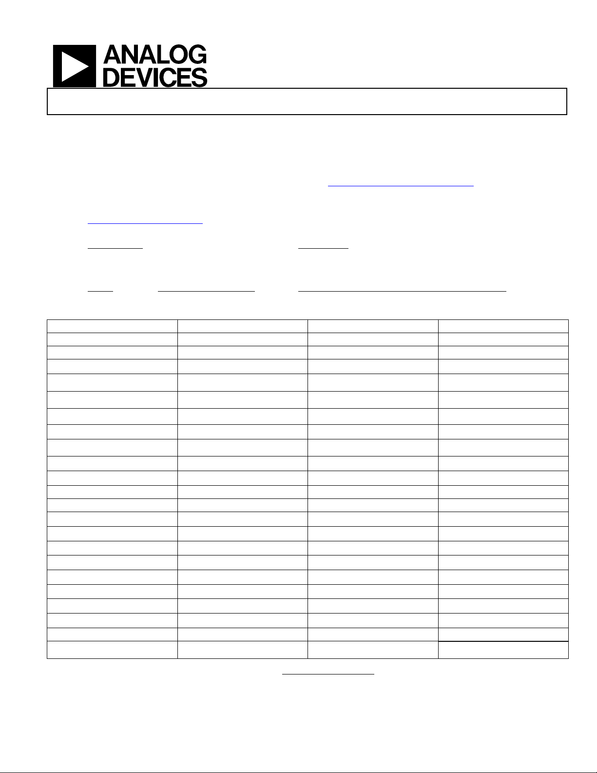
3.0 Terminal Connections:
Pin Number Mnemonic Pin Number Mnemonic
1 AIN 23 GND
2 GND 24 VDD
3 VDD 25
4
5
____________
DEMUX
____
DS
26
27
6 DS 28
7 ENCODE 29
8
_____________
ENCODE
30
9 VDD 31
10 GND 32
11 VDD 33 GND
12 GND 34 VDD
DA
DA
DA5
DA4
DA
DA
DA
DA0
7
6
35 GND
36 VDD
37 VDD
38 GND
3
2
1
39 VREF OUT
40 VREF IN
41 GND
42 VDD
13
14
15
16
17
18
19
20
21 VDD 43 GND
22 GND 44
Figure 1 - Terminal connections
.
DB0
DB
DB
DB3
DB4
DB
DB6
DB7
______
AIN
1
2
5
ASD0015375 Rev. D
Information furnished by Analog Devices is believed to be accurate and
reliable. However, no responsibility is assumed by Analog Devices for its use,
nor for any infringements of patents or other rights of third parties that may
result from its use. Specifications subject to change without notice. No license
is granted by implication or otherwise under any patent or patent rights of
Analog Devices. Trademarks and registered trademarks are the property of
their respective companies.
One Technology Way, P.O. Box 9106, Norwood, MA 02062-9106,
U.S.A.
Tel: 781.329.4700 www.analog.com
Fax: 781.326.8703 © 2008 Analog Devices, Inc. All rights reserved.
AD9054A
4.0 Absolute Maximum Ratings. (TA = 25°C, unless otherwise noted)
V
Analog Inputs.....................................................................................................V
Digital Inputs.....................................................................................................V
VREF IN, VREF OUT.......................................................................................V
…………....................................................................................................................6V
DD
to 0.0V
DD
to 0.0V
DD
to 0.0V
DD
Digital Output Current.................................................................................................20mA
Operating Temperature..............................................................................-55°C to +125°C
Storage Temperature..................................................................................-65°C to +150°C
Maximum Junction Temperature..............................................................................+150°C
Maximum Case Temperature ...................................................................................+150°C
NOTES
Absolute maximum ratings are limiting values to be applied individually, and beyond which the serviceability
of the circuit may be impaired. Functional operability is not necessarily implied. Exposure to absolute
maximum rating conditions for an extended period of time may affect device reliability.
4.1 Thermal Characteristics:
Thermal Resistance, 44-lead JLCC Package
Junction-to-Case (Θ
Junction-to-Ambient (Θ
) = 10°C/W Max
JC
) = 49°C/W Max
JA
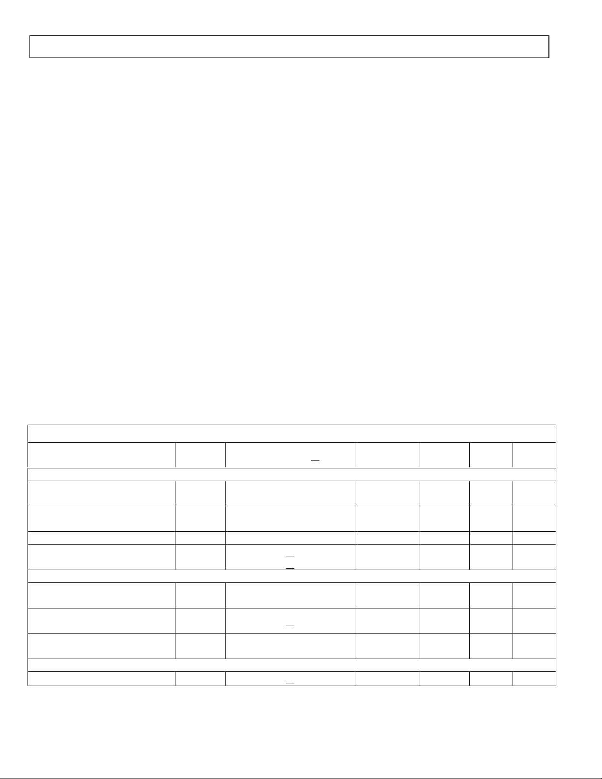
4.2 Electrical Table:
Table I
Parameter
See notes at end of table
Symbol Conditions 1/
Sub-
group
DC Accuracy
Differential Nonlinearity DNL
Integral Nonlinearity INL
1
2,3
1
2,3
No Missing Codes Guaranteed
Gain Error
A
e
8/
1
2,3
2/
Analog Input
Input Offset Voltage VOS
Input Resistance
Input Bias Current
R
in
I
b
8/
1
2,3
1
2,3
1
2,3
Reference Output
Output Voltage
V
REF
8/
1,2,3 2.4 2.6 V
Limit
Min
-1
-1
36
23
Limit
Max
+1.5
+2.0
±1.5
±2.0
±7.0
±9.0
±16
±23
kΩ
50
75
Units
LSB
LSB
%FS
mV
µA
ASD0015375 Rev. D | Page 2 of 5

Parameter
See notes at end of table
Switching Performance
Maximum Conversion Rate
Output Valid Time
Output Propagation Delay
Digital Inputs
HIGH Level Current
LOW Level Current
Digital Outputs
HIGH Output Voltage
LOW Output Voltage
Power Supply
V
Supply Current IDD
DD
Power Dissipation
Power Dissipation Sensitivity
Dynamic Performance
Signal-to-Noise Ratio
(Without Harmonics)
Signal-to-Noise Ratio
(With Harmonics)
Effective Number of Bits ENOB
2nd Harmonic Distortion 2HD
Symbol Conditions 1/
F
s
t
v
t
PD
I
IH
I
IL
V
OH
V
OL
P
D
P
SS
SNR
SINAD
Table I (Continued)
1,2,3 200 MSPS
3/
, 9/ 7 2.7 ns
3/
, 9/ 7 7.9 ns
4/
, 8/ 1,2,3 625 µA
4/
, 8/ 1,2,3 625 µA
9/
1,2,3 2.4 V
9/
1,2,3 0.4 V
8/
1,2,3 156 mA
5/
1 781 mW
6/
1 15 mV/V
= 49.7 MHZ
f
IN
f
= 70.1 MHZ
IN
= 49.7 MHZ
f
IN
f
= 70.1 MHZ
IN
= 49.7 MHZ
f
IN
f
= 70.1 MHZ
IN
= 49.7 MHZ
f
IN
f
= 70.1 MHZ
IN
Sub-
group
9
9
9
9
9
9
9
9
Limit
Min
42
42
40
39
6.35
6.18
54
49
AD9054A
Limit
Max
dB
dB
Bits
dBc
Units
= 49.7 MHZ
f
3rd Harmonic Distortion 3HD
TABLE I NOTES:
/ VDD = 5 V, external reference, fs = max unless otherwise noted.
1
/ Gain error and gain temperature coefficient are based on the ADC only (with a fixed 2.5 V external reference)
2
3/ t
outputs. The output ac load during test is 5 pF.
4
/ IIH and IIL are valid for differential input voltages of less than 1.5V. At higher differential voltages, the input current
will increase to a maximum of 1.5 mA at 25°C and 2.0 mA @ -55°C and 125°C
5
/ Power dissipation is measured under the following conditions: analog input is -1 dBFS at 19.7 MHz.
6
/ A change in input offset voltage with respect to a change in VDD.
/ SNR/harmonics based on an analog input voltage of -1.0 dBFS referenced to a 1.024 V full-scale input range.
7
8
/ 100% production tested at 25°C; guaranteed by design and characterization testing for full mil temperature range.
9
/ Go/No-Go parameter only, no read and record data available.
and tPD are measured from the threshold crossing of the ENCODE input to valid TTL levels of the digital
v
IN
f
= 70.1 MHZ
IN
ASD0015375 Rev. D | Page 3 of 5
9
9
48
43
dBc

AD9054A
4.3 Electrical Test Requirements:
Table II
Test Requirements Subgroups (in accordance with
MIL-PRF-38535, Table III)
Interim Electrical Parameters 1
Final Electrical Parameters 1, 2, 3, 7, 9 1/ 2/ 3/
Group A Test Requirements 1, 2, 3, 7, 9 3/
Group C end-point electrical parameters 1 2/
Group D end-point electrical parameters 1
1/ PDA applies to subgroup 1 only. Delta's excluded from PDA.
/ See Table III for delta parameters. See Table I for test conditions.
2
/ Table I parameters with Note 8/ are 100% production tested at 25°C; guaranteed by design and
3
characterization testing for full mil temperature range.
4.4 Table III - Life Test Endpoint and Delta Parameter (Product is tested in accordance with Table I
with the following exceptions)
Parameter Symbol
V
Supply Current
DD
I
DD
Input Offset Voltage VOS
Gain Error
A
Post Burn
Sub-
groups
1
1
e
1
in Limit
Max
156 - 171.6 ±15.6 mA
±23 ±7 ±30 ±7 mV
±9 ±2 ±13 ±4 %FS
Burn In
Delta
Post Life
Test Limit
Max
Life Test
Delta
Units
5.0 MIL-STD-38535 QMLV exceptions:
5.1 Full WLA per MIL-STD-883 TM 5007 is not available for this product fabricated in a
QMLQ wafer process facility. SEM Inspection only is available per MIL-STD-883,
TM2018.
ASD0015375 Rev. D | Page 4 of 5

Rev Description of Change Date
A Initiate 10/18/2004
B Typical values for Dynamic Performance for subgroup 10 & 11 deleted 06/15/2005
C
Clarify SEM vs. WLA availability for QMLQ fab process
11/12/2007
D Update header/footer and add to 1.0 Scope description. March 17, 2008
AD9054A
© 2008 Analog Devices, Inc. All rights reserved. Trademarks and
registered trademarks are the property of their respective
companies.
Printed in the U.S.A.
2/08
ASD0015375 Rev. D | Page 5 of 5
 Loading...