

查询AD9022供应商查询AD9022供应商
12-Bit 20 MSPS
a
FEATURES
Monolithic
12-Bit 20 MSPS A/D Converter
Low Power Dissipation: 1.4 Watts
On-Chip T/H and Reference
High Spurious-Free Dynamic Range
TTL Logic
APPLICATIONS
Radar Receivers
Digital Communications
Digital Instrumentation
Electro-Optics
PRODUCT DESCRIPTION
The AD9022 is a high speed, high performance, monolithic
12-bit analog-to-digital converter. All necessary functions, including track-and-hold (T/H) and reference, are included
on-chip to provide a complete conversion solution. It is a
companion unit to the AD9023; the primary difference between
the two is that all logic for the AD9022 is TTL-compatible,
while the AD9023 utilizes ECL logic for digital inputs and outputs. Pinouts for the two parts are nearly identical.
Operating from +5 V and –5.2 V supplies, the AD9022 provides excellent dynamic performance. Sampling at 20 MSPS
with A
typically 76 dB; with A
typically 65 dB.
The onboard T/H has a 110 MHz bandwidth and, more importantly, is designed to provide excellent dynamic performance for
analog input frequencies above Nyquist. This feature is necessary in many undersampling signal processing applications, such
as in direct IF-to-digital conversion.
To maintain dynamic performance at higher IFs, monolithic
RF track-and-holds (such as the AD9100 and AD9101
Samplifier™) can be used with the AD9022 to process signals
up to and beyond 70 MHz.
= 1 MHz, the spurious-free dynamic range (SFDR) is
IN
= 9.6 MHz, SFDR is 74 dB. SNR is
IN
Monolithic A/D Converter
AD9022
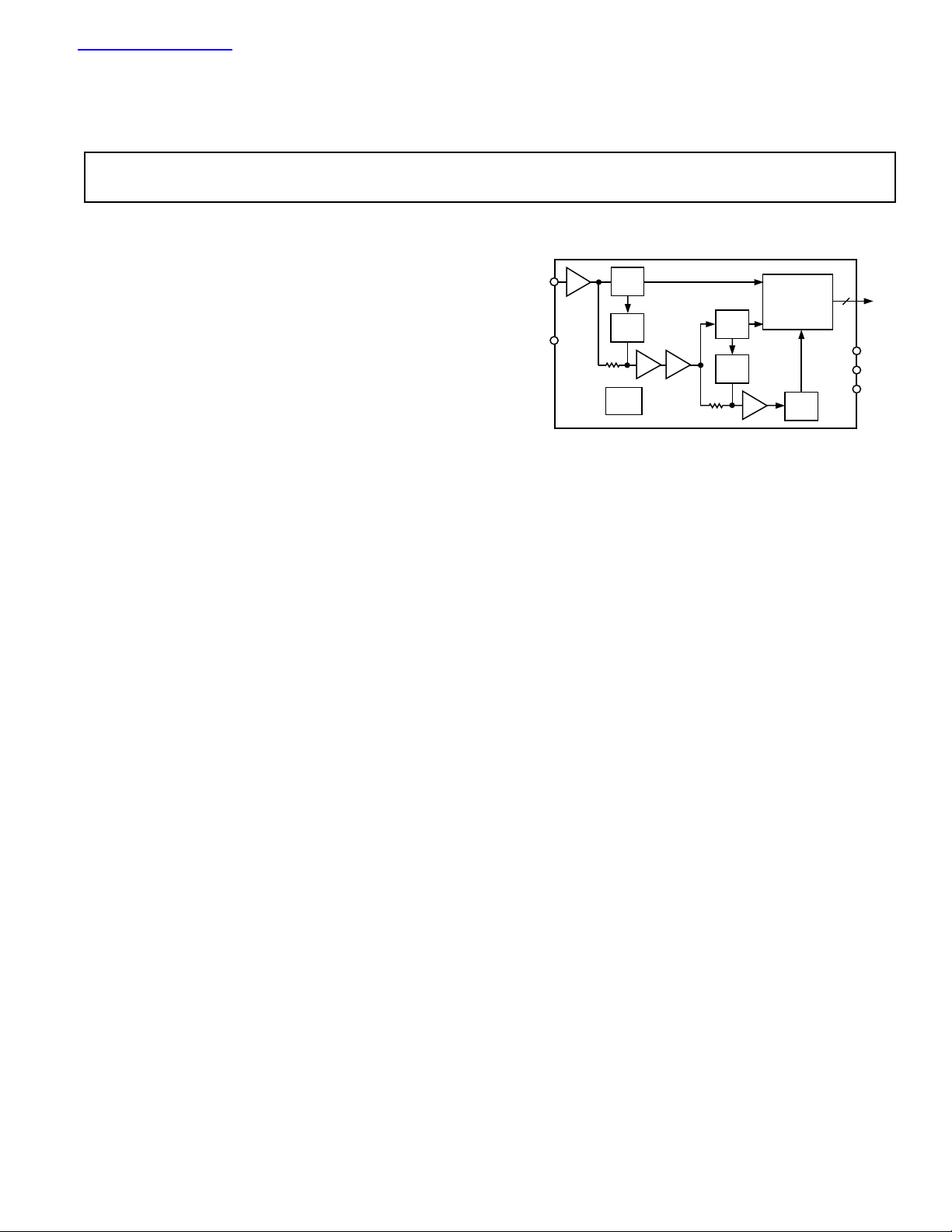
FUNCTIONAL BLOCK DIAGRAM
ANALOG
INPUT
ENCODE
With DNL typically less than 0.5 LSB and 20 ns transient response settling time, the AD9022 provides excellent results
when low-frequency analog inputs must be oversampled (such
as CCD digitization). The full scale analog input is ± 1 V with a
300 Ω input impedance. The analog input can be driven directly
from the signal source, or can be buffered by the AD96xx series
of low noise, low distortion buffer amplifiers.
All timing is internal to the AD9022; the clock signal initiates
the conversion cycle. For best results, the encode command
should contain as little jitter as possible. High speed layout
practices must be followed to ensure optimum A/D performance.
The AD9022 is built on a trench isolated bipolar process and
utilizes an innovative multipass architecture (see the block
diagram). The unit is packaged in 28-lead ceramic DIPs and
gullwing surface mount packages. The AD9022 is specified to
operate over the industrial (–25°C to +85°C) and military
(–55°C to +125°C) temperature ranges.
T/H
5-BIT
ADC
DAC
+2V
REF
T/H
AD9022
16
5-BIT
ADC
DAC
DIGITAL
ERROR
CORRECTION
8
4-BIT
ADC
12
TTL
+5V
–5.2V
GND
Samplifier is a trademark of Analog Devices, Inc.
REV. B
Information furnished by Analog Devices is believed to be accurate and
reliable. However, no responsibility is assumed by Analog Devices for its
use, nor for any infringements of patents or other rights of third parties
which may result from its use. No license is granted by implication or
otherwise under any patent or patent rights of Analog Devices.
One Technology Way, P.O. Box 9106, Norwood, MA 02062-9106, U.S.A.
Tel: 781/329-4700 World Wide Web Site: http://www.analog.com
Fax: 781/326-8703 © Analog Devices, Inc., 1998

AD9022–SPECIFICA TIONS
ELECTRICAL CHARACTERISTICS
Parameter (Conditions) Temp Level Min Typ Max Min Typ Max Min Typ Max Units
RESOLUTION 12 12 12 Bits
DC ACCURACY
Differential Nonlinearity +25°C I 0.6 0.75 0.4 0.5 0.6 0.75 LSB
Full VI 1.0 1.0 1.0 LSB
Integral Nonlinearity +25°C I 1.3 2.5 1.3 2.0 1.3 2.5 LSB
Full VI 1.6 3.0 1.6 3.0 1.6 3.0 LSB
No Missing Codes Full VI Guaranteed Guaranteed Guaranteed
Offset Error +25°CI 525 525 525 mV
Full VI 15 35 15 35 15 35 mV
Gain Error +25°C I 0.5 2.5 0.5 2.5 0.5 2.5 % FS
Full VI 0.6 3.5 0.6 3.5 0.6 3.5 % FS
Thermal Noise +25°C V 0.57 0.57 0.57 LSB, rms
ANALOG INPUT
Input Voltage Range ±1.024 ±1.024 ±1.024 V
Input Resistance Full IV 240 300 360 240 300 360 240 300 360 Ω
Input Capacitance +25°CV 5 5 5 pF
Analog Bandwidth +25°C V 110 110 110 MHz
SWITCHING PERFORMANCE
Minimum Conversion Rate +25°C IV 4 4 4 MSPS
Maximum Conversion Rate Full VI 20 20 20 MSPS
Aperture Delay (t
Aperture Uncertainty (Jitter) +25°C V 6 6 6 ps, rms
Output Delay (tOD) Full VI 15 27.5 15 27.5 15 27.5 ns
) +25°C IV 0.55 0.71 0.85 0.55 0.71 0.85 0.55 0.71 0.85 ns
A
1
(+VS = +5 V; –VS = –5.2 V; Encode = 20 MSPS, unless otherwise noted)
Test AD9022AQ/AZ AD9022BQ/BZ AD9022SQ/SZ
ENCODE INPUT
Logic Compatibility TTL TTL TTL
Logic “1” Voltage Full VI 2.0 2.0 2.0 V
Logic “0” Voltage Full VI 0.8 0.8 0.8 V
Logic “1” Current Full VI 8 20 8 20 8 20 µA
Logic “0” Current Full VI 8 20 8 20 8 20 µA
Input Capacitance +25°CV 6 6 6 pF
Pulsewidth (High) +25°C IV 22.5 125 22.5 125 22.5 125 ns
Pulsewidth (Low) +25°C IV 20 125 20 125 20 125 ns
DYNAMIC PERFORMANCE
Transient Response +25°C V 20 20 20 ns
Overvoltage Recovery Time +25°C V 20 20 20 ns
Harmonic Distortion
Analog Input @ 1.2 MHz +25°C I 65 73 70 75 65 73 dBc
@ 1.2 MHz Full V 70 72 70 dBc
@ 4.3 MHz +25°C V 73 75 73 dBc
@ 9.6 MHz +25°C I 63 72 69 74 63 72 dBc
@ 9.6 MHz Full V 68 72 68 dBc
Signal-to-Noise Ratio
Analog Input @ 1.2 MHz +25°C I 62 64 64 66 62 64 dB
Signal-to-Noise Ratio
(Without Harmonics)
Analog Input @ 1.2 MHz +25°C I 63 66 65 67 63 66 dB
2
@ 1.2 MHz Full V 63 65 63 dB
@ 4.3 MHz +25°C V 64 66 64 dB
@ 9.6 MHz +25°C I 61 63 63 65 61 63 dB
@ 9.6 MHz Full V 62 63 62 dB
2
@ 1.2 MHz Full V 64 66 64 dB
@ 4.3 MHz +25°C V 66 66 66 dB
@ 9.6 MHz +25°C I 62 65 64 66 62 65 dB
@ 9.6 MHz Full V 63 65 63 dB
–2–
REV. B
AD9022
Test AD9022AQ/AZ AD9022BQ/BZ AD9022SQ/SZ
Parameter (Conditions) Temp Level Min Typ Max Min Typ Max Min Typ Max Units
Two-Tone Intermodulation
Distortion Rejection
DIGITAL OUTPUTS
Logic Compatibility TTL TTL TTL
Logic “1” Voltage Full VI 2.4 2.4 2.4 V
Logic “0” Voltage Full VI 0.5 0.5 0.5 V
Output Coding Offset Binary Offset Binary Offset Binary
POWER SUPPLY
+V
Supply Voltage Full VI 4.75 5.0 5.25 4.75 5.0 5.25 4.75 5.0 5.25 mA
S
+VS Supply Current Full VI 100 120 100 120 100 120 mA
–V
Supply Voltage Full VI –5.45 –5.2 –4.95 –5.45 –5.2 –4.95 –5.45 –5.2 –4.95 mA
S
–VS Supply Current Full VI 180 220 180 220 180 220 mA
Power Dissipation Full VI 1.4 1.9 1.4 1.9 1.4 1.9 W
Power Supply
Rejection Ratio (PSRR)
NOTES
1
AD9022 load is a single LS latch.
2
RMS signal-to-rms noise with analog input signal 1 dB below full scale at specified frequency. Tested at 55% duty cycle.
3
Intermodulation measured with analog input frequencies of 8.9 MHz and 9.8 MHz at 7 dB below full scale.
4
PSRR is sensitivity of offset error to power supply variations within the 5% limits shown.
Specifications subject to change without notice.
3
1
4
+25°C V 74 74 74 dBc
Full V 32 32 32 mV/V
N
ANALOG
ENCODE
DATA
OUTPUT
IN
t
a
t
= 0.7 TYPICAL
a
t
OD
t
OD
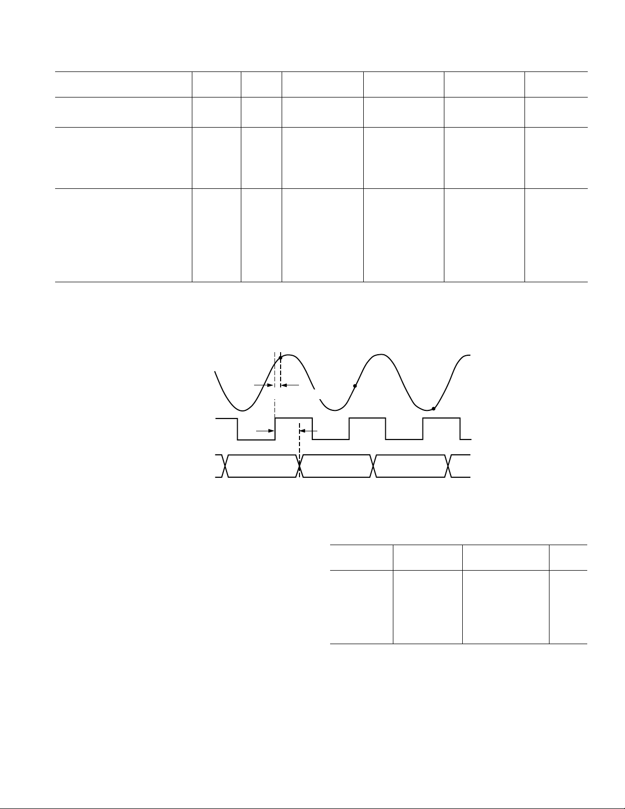
AD9022 Timing Diagram
ABSOLUTE MAXIMUM RATINGS
1
+VS . . . . . . . . . . . . . . . . . . . . . . . . . . . . . . . . . . . . . . . . . +6 V
–V
. . . . . . . . . . . . . . . . . . . . . . . . . . . . . . . . . . . . . . . . . .–6 V
S
Analog Input . . . . . . . . . . . . . . . . . . . . . . . . . –1.5 V to +1.5 V
Digital Inputs . . . . . . . . . . . . . . . . . . . . . . . . . . . . .+V
to 0 V
S
Digital Output Current . . . . . . . . . . . . . . . . . . . . . . . . . 20 mA
Operating Temperature Range
AD9022AQ/AZ/BQ/BZ . . . . . . . . . . . . . . . –25°C to +85°C
AD9022SQ/SZ . . . . . . . . . . . . . . . . . . . . . –55°C to +125°C
Maximum Junction Temperature
2
. . . . . . . . . . . . . . . . +175°C
Lead Temperature (Soldering, 10 sec) . . . . . . . . . . . . +300°C
Storage Temperature Range . . . . . . . . . . . . –65°C to +150°C
NOTES
1
Absolute maximum ratings are limiting values to be applied individually, and
beyond which the serviceability of the circuit may be impaired. Functional
operability is not necessarily implied. Exposure to absolute maximum rating
conditions for an extended period of time may affect device reliability.
2
Typical thermal impedances: “Q” Package (Ceramic DIP): θJC = 10°C/W; θJA =
35°C/W. “Z” Package (Gullwing Surface Mount): θJC = 13°C/W; θJA = 45°C/W.
N + 1
N + 2
= 15–27.5 TYPICAL
N – 2 N – 1
NN – 3
ORDERING GUIDE
Temperature Package Package
Model Range Description Option
AD9022AQ/BQ –25°C to +85°C 28-Lead Ceramic DIP Q-28
AD9022AZ/BZ –25°C to +85°C 28-Pin Ceramic Z-28
Leaded Chip Carrier
AD9022SQ –55°C to +125°C 28-Lead Ceramic DIP Q-28
AD9022SZ –55°C to +125°C 28-Pin Ceramic Z-28
Leaded Chip Carrier
REV. B
–3–

AD9022
EXPLANATION OF TEST LEVELS
Test Level
I – 100% production tested.
II – 100% production tested at +25°C, and sample tested at
specified temperatures. AC testing done on sample basis.
III – Sample tested only.
IV – Parameter is guaranteed by design and characterization
testing.
V – Parameter is a typical value only.
VI – All devices are 100% production tested at +25°C. 100%
production tested at temperature extremes for extended
temperature devices; guaranteed by design and character-
ization testing for industrial devices.
DIE LAYOUT AND MECHANICAL INFORMATION
Die Dimensions . . . . . . . . . . . . . . . . 205 × 228 × 21 (±1) mils
Pad Dimensions . . . . . . . . . . . . . . . . . . . . . . . . . . . . 4 × 4 mils
Metalization . . . . . . . . . . . . . . . . . . . . . . . . . . . . . . Aluminum
Backing . . . . . . . . . . . . . . . . . . . . . . . . . . . . . . . . . . . . . None
Substrate Potential . . . . . . . . . . . . . . . . . . . . . . . . . . . . . . –V
S
Transistor Count . . . . . . . . . . . . . . . . . . . . . . . . . . . . . . 4,080
Passivation . . . . . . . . . . . . . . . . . . . . . . . . . . . . . . . Oxynitride
Bond Wire . . . . . . . . . . . . . . . . . . . . . . . . . . . . . . . Aluminum
PIN FUNCTION DESCRIPTIONS
Pin No. Name Function
1–3 D3–D1 Digital output bits of ADC; TTL
compatible.
4 D0 (LSB) Least significant bit of ADC output;
TTL compatible.
5 NC No Connection Internally
6+V
S
+5 V Power Supply
7 GND Ground
8 ENCODE Encode clock input to ADC. Internal
T/H is placed in hold mode (ADC is
encoding) on rising edge of encode
signal.
9 GND Ground
10 +V
S
+5 V Power Supply
11 GND Ground
12 A
13 –V
14 +V
15 –V
IN
S
S
S
Noninverting input to T/H amplifier.
–5.2 V Power Supply
+5 V Power Supply
–5.2 V Power Supply
16 GND Ground
17 COMP Should be connected to –V
through
S
0.1 µF capacitor.
18 D11 (MSB) Most significant bit of ADC output;
TTL compatible.
19–25 D10–D4 Digital output bits of ADC; TTL
compatible.
26 +V
27 –V
S
S
+5 V Power Supply
–5.2 V Power Supply
28 GND Ground
–4–
PIN DESIGNATIONS
D3
1
2
D2
3
D1
D0 (LSB)
ENCODE
4
5
NC
6
+V
S
AD9022
7
GND
GND
GND
NC = NO CONNECT
COMPENSATION (PIN 17) SHOULD BE
CONNECTED TO –V
+V
A
IN
–V
+V
8
9
10
S
11
12
13
S
14
S
TOP VIEW
(Not to Scale)
S
GND
28
27
–V
S
26
+V
S
25
D4
24
D5
D6
23
22
D7
D8
21
D9
20
D10
19
D11(MSB)
18
COMP
17
GND
16
–V
15
S
THROUGH 0.01mF
REV. B

DEFINITIONS OF SPECIFICATIONS
p
Analog Bandwidth
The analog input frequency at which the spectral power of the
fundamental frequency (as determined by FFT analysis) is
reduced by 3 dB.
Aperture Delay
The delay between the rising edge of the ENCODE command
and the instant at which the analog input is sampled.
Aperture Uncertainty (Jitter)
The sample-to-sample variation in aperture delay.
Differential Nonlinearity
The deviation of any code from an ideal 1 LSB step.
Harmonic Distortion
The rms value of the fundamental divided by the rms value of
the worst harmonic component.
Integral Nonlinearity
The deviation of the transfer function from a reference line
measured in fractions of 1 LSB using a “best straight line” determined by a least square curve fit.
Minimum Conversion Rate
The encode rate at which the SNR of the lowest analog signal
frequency tested drops by no more than 3 dB below the guaranteed limit.
Maximum Conversion Rate
The encode rate at which parametric testing is performed.
Output Propagation Delay
The delay between the 50% point of the rising edge of the ENCODE command and the time when all output data bits are
within valid logic levels.
Overvoltage Recovery Time
The amount of time required for the converter to recover to
12-bit accuracy after an analog input signal 150% of full scale is
reduced to the full-scale range of the converter.
Power Supply Rejection Ratio (PSRR)
The ratio of a change in input offset voltage to a change in
power supply voltage.
Signal-to-Noise Ratio (SNR)
The ratio of the rms signal amplitude to the rms value of
“noise,” which is defined as the sum of all other spectral components, including harmonics but excluding dc, with an analog
input signal 1 dB below full scale.
Signal-to-Noise Ratio (Without Harmonics)
The ratio of the rms signal amplitude to the rms value of
“noise,” which is defined as the sum of all other spectral components, excluding the first five harmonics and dc, with an analog
input signal 1 dB below full scale.
Transient Response
The time required for the converter to achieve 12-bit accuracy
when a step function is applied to the analog input.
Two-Tone Intermodulation Distortion (IMD) Rejection
The ratio of the power of either of two input signals to the
power of the strongest third-order IMD signal.
+V
S
ANALOG
INPUT
180V
120V
–V
Analog Input
+V
100V
ENCODE
900V
–V
Encode Input
COMPENSATION
50V
20pF
–V
S
Compensation
+V
S
11kV 12kV
DIGITAL
OUTPUT
–V
S
Out
ut Stage
Figure 1. Equivalent Circuits
AD9022
+V
S
10pF
S
S
S
–V
S
REV. B
–5–

AD9022
–Typical Performance Characteristics
–76
–75
–74
–73
–72
–71
–70
–69
WORST CASE HARMONIC DISTORTION – dBc
–68
0101
23456789
ANALOG INPUT FREQUENCY – MHz
+258C
ROOM
–558C
+1258C
Figure 2. Harmonic Distortion vs. Analog Input
Frequency
85
AIN = 1.2MHz
80
75
70
65
HARMONICS AND SNR – dB
60
55
5.0
7.5 10.0 12.5 17.515.0 20.0 22.5 25.0
WORST HARMONICS
SNR
ENCODE RATE – MSPS
Figure 3. SNR and Harmonics vs. Encode Rate
70
65
60
55
50
SNR – dB
45
40
35
1.24
2.3
ANALOG INPUT FREQUENCY – MHz
+258C
–558C
+1258C
17.315.313.39.67.35.3 11.3
19.3
Figure 5. Signal-to-Noise Ratio vs. Analog Input
Frequency
90
AIN = 1.2MHz
80
ENCODE = 20MHz
70
60
50
40
30
SFDR AND SNR – dB
20
10
0
–45–50
SFDR
SNR
INPUT LEVEL – dB
–5–10–15–20–25–30–35–40
–1
Figure 6. SFDR and SNR vs. Analog Input Level
2.0
A
= 1.2MHz
1.5
1.0
0.5
0
–0.5
–1.0
–1.5
DIFFERENTIAL NONLINEARITY – LSBs
–2.0
1024
OUTPUT CODE
IN
= 20MSPS
F
S
30722048
4096
Figure 4. Differential Nonlinearity vs. Output Code
–6–
80
AIN = 9.6MHz
70
ENCODE = 20MHz
60
50
40
30
SFDR AND SNR – dB
20
10
0
–45–50
SFDR
INPUT LEVEL – dB
SNR
–1
–5–10–15–20–25–30–35–40
Figure 7. SFDR and SNR vs. Analog Input Level
REV. B

AD9022
0
–10
–20
–30
–40
–50
–60
FULL SCALE – dB
–70
–80
–90
–100
0
FREQUENCY – MHz
AIN = 1.2MHz
A
= –1.0dBFS
IN
SNR = 66.7dB
THD = 77.51dB
SFDR = 79.49dBFS
10
Figure 8. FFT Plot
0
AIN = 9.6MHz
–10
A
= –1.0dBFS
IN
SNR = 66.05dB
–20
THD = 74.28dB
SFDR = 75.32dBFS
–30
–40
–50
–60
FULL SCALE – dB
–70
–80
–90
–100
0
FREQUENCY – MHz
10
Figure 9. FFT Plot
0
A
= 8.9MHz
IN1
A
= 9.8MHz
IN2
20
A
= 7.0dBFS
IN1
A
= 7.0dBFS
IN2
SFDR = 80.62dBFS
40
60
FULL SCALE – dB
80
100
120
FREQUENCY – MHz
10.00.0 8.06.04.02.0
Figure 10. Two-Tone FFT
THEORY OF OPERATION
Refer to the block diagram.
The AD9022 employs a three-pass subranging architecture and
digital error correction. This combination of design techniques
ensures 12-bit accuracy at relatively low power.
Analog input signals are immediately attenuated through a
resistor divider and applied directly to the sampling bridge of
the track-and-hold (T/H). The T/H holds whatever analog value
is present when the unit is strobed with an ENCODE command. The conversion process begins on the rising edge of this
pulse, which should conform to the minimum and maximum
pulsewidth requirements shown in the specifications. Operation
below the recommended encode rate (4 MSPS) may result in
excessive droop in the internal T/H devices–leading to large dc
and ac errors.
The held analog value of the first track-and-hold is applied to a
5-bit flash converter and a second T/H. The 5-bit flash converter resolves the most significant bits (MSBs) of the held
analog voltage. These five bits are reconstructed via a 5-bit
DAC and subtracted from the original T/H output signal to
form a residue signal.
A second T/H holds the amplified residue signal while it is encoded with a second 5-bit flash ADC. Again the five bits are
reconstructed and subtracted from the second T/H output to
form a residue signal. This residue is amplified and encoded
with a 4-bit flash ADC to provide the three least significant bits
(LSBs) of the digital output and one bit of error correction.
Digital Error Correction logic aligns the data from the three
flash converters and presents the result as a 12-bit parallel digital word. The output stage of the AD9022 is TTL. Output data
may be strobed on the rising edge of the ENCODE command.
AD9022 IN RECEIVER APPLICATIONS
Advances in semiconductor processes have resulted in low cost
digital signal processing (DSP) and analog signal processing
which can help create cost effective alternative receiver designs.
Today, an all-digital receiver allows tuning, demodulation, and
detection of receiver signals in the digital domain. By digitizing
IF signals directly, and utilizing digital techniques, it becomes
possible to make significant improvements in receiver design.
For high frequency IFs, the ADC is the key to the receiver’s
performance. Unfortunately, the specifications frequently used
by receiver designers and analog-to-digital (ADC) manufacturers are often very different. Noise Figure and Intercept Point are
common measures of noise and linearity in analog RF system
design. ADCs are more frequently specified in terms of SNR
and harmonic distortion.
Noise
Noise figure (NF) is a measure of receiver sensitivity and is
defined as the degradation of signal-to-noise ratio (SNR) as a
signal passes through a device. In equation form:
NF = SNR (in) – SNR (out)
Noise figure is a bandwidth invariant parameter for reasonably
narrow bandwidths in most devices. The system noise figure for
a combination of amplifiers and mixers, for instance, can be
analyzed without regard to the information bandwidth.
Thermal noise contribution from the ADC behaves in a similar
fashion; however, the spectral density of quantization noise is a
function of the sample rate. In addition, the spectral density of
the quantization noise is flat only in an ADC with perfect linearity, i.e., perfect 1 LSB step sizes.
To analyze the system noise performance, ADC noise figure is
calculated by normalizing the SNR of the ADC output to a 1 Hz
bandwidth. This result is given by:
where F
SNR (/Hz) = SNR + 10 log
is the sample rate.
S
(FS/2)
10
REV. B
–7–

AD9022
This will be true only for converters in which perfect quantization noise dominates. There may be an upper sample rate,
above which the thermal noise of the converter is the dominant
source of noise. In this case, normalization would be based on
the noise bandwidth of the ADC. For an AD9022 with a typical
SNR of 64 dB and a sample rate of 20 MSPS, the normalized
SNR is equal to 134 dB (64 + 70). Both thermal and quantization noise contribute to this number.
The SNR of the input is assumed to be limited by the thermal
noise of the input resistance, or –174 dBm/Hz. The input signal
level is +10 dBm (2 V p-p into 50 Ω). Noise figure of the ADC
can be calculated by:
NF = SNR (in) – SNR (out) = [+10 – (174)] – 134 = 50 dB
Most ADCs detect input voltage levels, not power. Consequently, the input SNR can be determined more accurately by
determining the ratio of the signal voltage to the noise voltage of
the terminating resistor. However, both the input signal and
noise voltage delivered to the ADC are also a function of the
source impedance. The dependence of NF on sample rate,
linearity, source and terminating impedances, and the number
of assumptions required, highlight the weakness of using NF as
a figure of merit for an ADC. The rather large number that
results bolsters this belief by indicating the ADC is often the
weakest link in the signal processing path.
Linearity
The Third Order intercept point for a linear device (with some
nonlinearity) is a good way to predict 3rd order spurious signals
as a function of input signal level. For an ADC, however, this in
an invalid concept except with signals near full scale. As the
input signal is reduced, the performance burden shifts from the
input track-and-hold (T/H) to the encoder. This creates a nonlinear function, as contrasted with the third order intercept
behavior, which predicts an improvement in dynamic range as
the signal level is decreased.
For signals near full scale, the intercept point is calculated the
same as any device:
Intercept Point = [Harmonic Suppression/(N –1)] + Input Power
where N = the order of the IMD (3 in this case)
AD9022 Intercept Point = 80/2 + 3 dBm (7 dBm below full scale)
= 43 dBm
For signals below this level, the spurious free dynamic range
(SFDR) curves shown in the data sheet are a more accurate
predictor of dynamic range. The SFDR curve is generated by
measuring the ratio of the signal (either tone in the two-tone
measurement) to the worst spurious signal, which is observed as
the analog input signal amplitude is swept.
The worst spurious signal is usually the second harmonic or 3rd
order IMD. Actual results are shown on several plots. The
straightline with a slope of one is constructed at the point where
the worst SFDR touches the line. This line, extrapolated to full
scale, gives the SFDR of the ADC. This value can then be used
to predict the dynamic range by simply subtracting the input
level from the SFDR.
It should be noted that all SFDR lines are constructed to be
valid only below a certain level below full scale. Above these
points, the linearity of the device is dominated by the nonlinearities
of the front end and best predicted by the intercept point.
AD9022 NOISE PERFORMANCE
High speed, wide bandwidth ADCs such as the AD9022 are
optimized for dynamic performance over a wide range of analog
input frequencies. However, there are many applications (Imaging, Instrumentation, etc.) where dc precision is also important.
Due to the wide input bandwidth of the AD9022 for a given
input voltage, there will be a range of output codes which may
occur. This is caused by unavoidable circuit noise within the
wideband circuits in the ADC. If a dc signal is applied to the
ADC and several thousand outputs are recorded, a distribution
of codes such as that shown in the histogram below may result.
2.0
0
x–3
ONE STANDARD
DEVIATION = RMS
NOISE LEVEL
x–2 x–1 x x+1 x+2 x+3
OUTPUT CODE
1.5
1.0
0.5
–0.5
–1.0
–1.5
RELATIVE FREQUENCY OF OCCURRENCE
–2.0
Figure 11. ADC Equivalent Input Noise
The correct code appears most of the time, but adjacent codes
also appear with reduced probability. If a normal probability
density curve is fitted to this Gaussian distribution of codes, the
standard deviation will be equal to the equivalent input rms
noise of the ADC. The rms noise may also be approximated by
converting the SNR, as measured by a low frequency FFT, to
an equivalent input noise. This method is accurate only if the
SNR performance is dominated by random thermal noise (the
low frequency SNR without harmonics is the best measure).
Sixty-three dB equates to 1 LSB rms for a 2 V p-p (0.707 V
rms) input signal. The AD9022 has approximately 0.5 LSB of
rms noise or a noise limited SNR of 69 dB, indicating that noise
alone does not limit the SNR performance of the device (quantization noise and linearity are also major contributors).
This thermal noise may come from several sources. The drive
source impedance should be kept low to minimize resistor
thermal noise. Some of the internal ADC noise is generated in
the wideband T/H. Sampling ADCs generally have input bandwidths which exceed the Nyquist frequency of one-half the
sampling rate. (The AD9022 has an input bandwidth of over
100 MHz, even though the sampling rate is limited to 20 MSPS.)
Wide bandwidth is required to minimize gain and phase distortion and to permit adequate settling times in the internal amplifiers and T/Hs. But a certain amount of unavoidable noise is
generated in the T/H and other wideband circuits within the
ADC; this causes variation in output codes for dc inputs. Good
layout, grounding and decoupling techniques are essential to
prevent external noise from coupling into the ADC and further
corrupting performance.
–8–
REV. B

AD9022
USING THE AD9022
Layout Information
Preserving the accuracy and dynamic performance of the
AD9022 requires that designers pay special attention to the
layout of the printed circuit board.
Analog paths should be kept as short as possible and be properly
terminated to avoid reflections. The analog input connection
should be kept away from digital signal paths; this reduces the
amount of digital switching noise, which is capacitively coupled
into the analog section. Digital signal paths should also be kept
short, and run lengths should be matched to avoid propagation
delay mismatch. The AD9022 digital outputs should be buffered or latched close to the device (<2 cm). This prevents load
transients that may feed back into the device.
In high speed circuits, layout of the ground is critical. A single,
low impedance ground plane on the component side of the
board is recommended. Power supplies should be capacitively
coupled to the ground plane with high quality 0.1 µF chip ca-
pacitors to reduce noise in the circuit. All power pins of the
AD9022 should be bypassed individually. The compensation
pin (COMP Pin 17) should be bypassed directly to the –V
S
supply (Pin 15) as close to the part as possible using a 0.1 µF
chip capacitor.
Multilayer boards allow designers to lay out signal traces without interrupting the ground plane, and provide low impedance
ground planes. In systems with dedicated analog and digital
grounds, all grounds for the AD9022 should be connected to
the analog ground plane.
In systems using multilayer boards, dedicated power planes are
recommended to provide low impedance connections for device
power. Sockets limit dynamic performance and are not recommended for use with the AD9022.
Timing
Conversion by the AD9022 is initiated by the rising edge of the
ENCODE clock (Pin 8). All required timing is generated internal to the ADC. Care should be taken to ensure that the encode
clock to the AD9022 is free from jitter that can degrade dynamic performance. The clock driver should be compatible with
TTL LS logic series devices. Drivers with excessive slew rate or
overdrive will degrade the dynamic performance of the AD9022.
Pulsewidth of the ADC encode clock must be controlled to
ensure the best possible performance. Dynamic performance is
guaranteed with a clock pulse HIGH minimum of 25 ns. Operation with narrower pulses will degrade SNR and dynamic performance. From a system perspective, this is generally not a
problem, because a simple inverter can be used to generate a
suitable clock if the system clock is less than 25 ns wide.
The AD9022 provides latched data outputs. Data outputs are
available two pipeline delays and one propagation delay after the
rising edge of the encode clock (refer to the AD9022 Timing
Diagram). The length of the output data lines and the loads
placed on them should be minimized to reduce transients within
the AD9022; these transients can detract from the converter’s
dynamic performance.
Operation at encode rates less than 4 MSPS is not recommended. The internal track-and-hold saturates, causing erroneous conversions. This T/H saturation precludes clocking the
AD9022 in a burst mode.
The duty cycle of the encode clock for the AD9022 is critical for
obtaining rated performance of the ADC. Internal pulsewidths
within the track-and-hold are established by the encode command pulsewidth; to ensure rated performance, minimum and
maximum pulsewidth restrictions should be observed. Operation at
20 MSPS is optimized when the duty cycle is held at 55%.
Analog Input
The analog input (Pin 12) voltage range is nominally ±1.024
volts. The range is set with an internal voltage reference and
cannot be adjusted by the user. The input resistance is 300 Ω
and the analog bandwidth is 110 MHz, making the AD9022
useful in undersampling applications.
The AD9022 should be driven from a low impedance source.
The noise and distortion of the amplifier should be considered
to preserve the dynamic range of the AD9022.
Power Supplies
The power supplies of the AD9022 should be isolated from the
supplies used for noisy devices (digital logic especially) to reduce the amount of noise coupled into the ADC. For optimum
performance, linear supplies ensure that switching noise from
the supplies does not introduce distortion products during
the encoding process. If switching supplies must be used,
decoupling recommendations above are critically important.
The PSRR of the AD9022 is a function of the ripple frequency
present on the supplies. Clearly, power supplies with the lowest
possible frequency should be selected.
AD9022 EVALUATION BOARD
The evaluation board for the AD9022 (AD9022/PCB) provides
an easy and flexible method for evaluating the ADC’s performance without (or prior to) developing a user-specific printed
circuit board. The two-sided board includes a reconstruction
DAC and digital output interface, and uses the layout and applications suggestions outlined above. It is available at nominal
cost from Analog Devices, Inc.
Input/Output/Supply Information
Power supply, analog input, clock connections and reconstructed output (RC OUTPUT) are identified by labels on the
evaluation board.
Operation of the evaluation board will conform to the following
characteristics:
Parameter Typical Units
Supply Current
+5 V 150 mA
–5 V 300 mA
A
IN
Impedance 51 Ω
Voltage Range ± 1.024 V
CLOCK
Impedance 51 Ω
Frequency 20 MSPS
RC OUTPUT
Impedance 51 Ω
Voltage Range 0 to –1 V
REV. B
–9–

AD9022
Analog Input
Analog input signals can be directly fed into the device under
test input (A
). The AIN input is terminated at the device with
IN
a 62 Ω resistor to give a parallel equivalent of 51 Ω (62 Ωi300 Ω).
DAC Reconstruction
The AD9022 evaluation board provides an onboard AD9713B
reconstruction DAC for observing the digitized analog input
2
3
4
5
6
7
8
9
2
3
4
5
6
7
8
9
C12
0.1mF
C20
0.1mF
74LS574
1D
2D
3D
4D
5D
6D
7D
8D
CK
11 1
74LS574
1D
2D
3D
4D
5D
6D
7D
8D
CK
11
CLOCK
A
IN
BNC
J1
+5V
BNC
J2
+5V
–5.2V
R1
51V
R2
5.1kV
C1
0.1mF
CR1
AD589H
C2
10mF
20%
35V
C3
10mF
20%
35V
R7
62V
U2
AD9698R
5
6
E2 E1
AD9698R
4
3
16
1
2
C6
0.1mF
C14
0.1mF
9
U2
R21
100V
12
14
13
11
C7
0.1mF
C15
0.1mF
CLK
9
10
U6
74AS32
C8
0.1mFC90.1mF
C16
0.1mF
U1
AD9022Q
D9
D10
D11
D12 LSB
8
8
ENCODE
12
IN
A
C17
0.1mF
MSB D1
COMP
C10
0.1mF
C18
0.1mF
D8
D7
D6
D5
D4
D3
D2
0.1mF
25
24
23
22
21
20
19
18
17
C4
–5.2V
C11
0.1mF
C19
0.1mF
signal. The AD9713B is terminated into 51 Ω to provide a
1 V p-p signal at the output (RC Output).
Output Data
The output data bits are latched with two 74LS574 latches
which drive a 40-pin connector (AMP p/n 102153-09). The
data and clock signals are available at the connector per the pin
assignments shown on the schematic of the evaluation board.
Data is latched on the rising edge of the encode clock.
U3
19
1Q
18
2Q
17
3Q
16
4Q
15
U4
C13
0.1mF
C21
0.1mF
OE
OE
5Q
6Q
7Q
8Q
1Q
2Q
3Q
4Q
5Q
6Q
7Q
8Q
14
13
12
D10
D9
D8
D7
19
18
17
16
15
14
13
12
1
C22
0.1mF
D6
D12
R8
D11
D5
D4
D3
J5
–5.2V
J6
+5V
J7
GND
R9
R10
R11
R12
R14
R15
R16
R17
R18
D2
R19
R20
D1
U6
74AS32
1
2
U6
74AS32
4
5
U6
74AS32
12
13
2
3
4
5
6
7
8
9
10
11
14
28
26
3
6
11
U5
AD9713P
D12 (LSB)
D11
REFOUT
D10
D9
D8
D7
D6
D5
D4
D3
D2
D1 (MSB)
LE
RSET
CIN
COUT
REFIN
IOUT
IOUT
CLK
D1
D2
D3
D4
D5
D6
D7
D8
D9
D10
D11
D12
24
20
19
18
17
0.1mF
16
14
R6
51V
H40DMC
J3
1
2
3
4
5
6
7
8
9
10
11
12
13
14
15
16
17
18
19
20
R4
7.5kV
R3
20V
C5
BNC
40
39
38
37
36
35
34
33
32
31
30
29
28
27
26
25
24
23
22
21
–5.2V
R5
51V
J4
RC
OUT
Figure 12. AD9022/PCB Evaluation Board Schematic
–10–
REV. B

AD9022
Figure 13. Top of Board, Viewed From Top
REV. B
Figure 14. Center of Board, Viewed From Top
–11–

AD9022
C1964a–0–1/98
Figure 15. Bottom of Board, Viewed from Bottom
28-Lead Cerdip
(Q-28)
0.005 (0.13) MIN
28
114
PIN 1
0.225
(5.72)
MAX
0.200 (5.08)
0.125 (3.18)
1.490 (37.85) MAX
0.026 (0.66)
0.014 (0.36)
0.110 (2.79)
0.090 (2.29)
0.100 (2.54) MAX
15
0.610 (15.49)
0.500 (12.70)
0.015
(0.38)
MIN
0.070 (1.78)
0.030 (0.76)
0.150
(3.81)
MIN
SEATING
PLANE
OUTLINE DIMENSIONS
Dimensions shown in inches and (mm).
0.165 (4.191)
MAX
0.620 (15.75)
0.590 (14.99)
0.018 (0.46)
0.008 (0.20)
15
0
0.115 (2.921)
MAX
28-Pin Ceramic Leaded Chip Carrier
(Z-28)
0.012 (0.305)
0.009 (0.229)
0.025
(0.635)
MIN
0.765 (19.431)
0.745 (18.923)
0.060 (1.524)
0.040 (1.016)
28
114
0.73 (18.544)
0.71 (18.036)
0.050 (1.27)
TYP
TOP VIEW
0.015 (0.381)
MIN
15
0.51 (12.954)
0.49 (12.446)
–12–
PRINTED IN U.S.A.
REV. B
 Loading...