

10-Bit 20 MSPS 160 mW
A/D
D/A
A/D
D/A A/D D/A
A/D
CORRECTION LOGIC
AIN
REFTF
REFTS
REFBS
REFBF
STBY
THREE-
STATE
(MSB)
D9
D0
(LSB)
DRV
DD
DV
DD
AV
DD
CLK
DRV
SS
DV
SS
AV
SS
CML
AD876
SHA SHA SHAGAIN SHA GAINGAIN
OUTPUT BUFFERS
a
FEATURES
CMOS 10-Bit 20 MSPS Sampling A/D Converter
Pin-Compatible 8-Bit Option
Power Dissipation: 160 mW
+5 V Single Supply Operation
Differential Nonlinearity: 0.5 LSB
Guaranteed No Missing Codes
Power Down (Standby) Mode
Three-State Outputs
Digital I/Os Compatible with +5 V or +3.3 V Logic
Adjustable Reference Input
Small Size: 28-Lead SOIC, 28-Lead SSOP, or 48-Lead
Thin Quad Flatpack (TQFP)
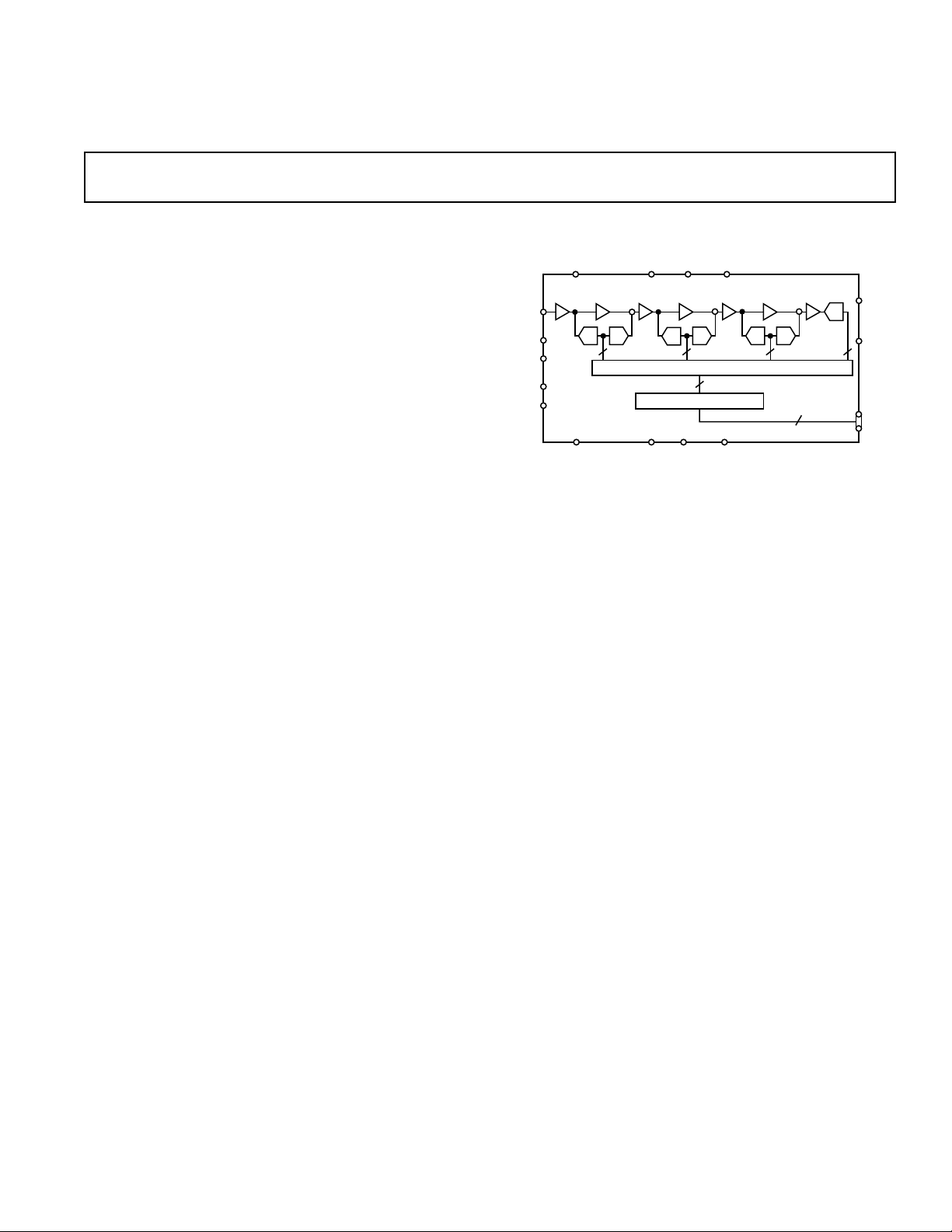
PRODUCT DESCRIPTION
The AD876 is a CMOS, 160 mW, 10-bit, 20 MSPS analog-todigital converter (ADC). The AD876 has an on-chip input
sample-and-hold amplifier. By implementing a multistage pipelined architecture with output error correction logic, the AD876
offers accurate performance and guarantees no missing codes
over the full operating temperature range. Force and sense connections to the reference inputs minimize external voltage drops.
The AD876 can be placed into a standby mode of operation
reducing the power below 50 mW. The AD876’s digital I/O
interfaces to either +5 V or +3.3 V logic. Digital output pins
can be placed in a high impedance state; the format of the output is straight binary coding.
The AD876’s speed, resolution and single-supply operation
ideally suit a variety of applications in video, multimedia, imaging, high speed data acquisition and communications. The
AD876’s low power and single-supply operation satisfy requirements for high speed portable applications. Its speed and resolution ideally suit charge coupled device (CCD) input systems
such as color scanners, digital copiers, electronic still cameras
and camcorders.
CMOS A/D Converter
AD876
FUNCTIONAL BLOCK DIAGRAM
The AD876 comes in a space saving 28-lead SOIC and 48-lead
thin quad flatpack (TQFP) and is specified over the commercial
(0°C to +70°C) temperature range.
PRODUCT HIGHLIGHTS
Low Power
The AD876 at 160 mW consumes a fraction of the power of
presently available 8- or 10-bit, video speed converters. Powerdown mode and single-supply operation further enhance its
desirability in low power, battery operated applications such
as electronic still cameras, camcorders and communication
systems.
Very Small Package
The AD876 comes in a 28-lead SOIC, 28-lead SSOP, and 48lead surface mount, thin quad flat package. The TQFP package
is ideal for very tight, low headroom designs.
Digital I/O Functionality
The AD876 offers three-state output control.
Pin Compatible Upgrade Path
The AD876 offers the option of laying out designs for eight
bits and migrating to 10-bit resolution if prototype results
warrant.
REV. B
Information furnished by Analog Devices is believed to be accurate and
reliable. However, no responsibility is assumed by Analog Devices for its
use, nor for any infringements of patents or other rights of third parties
which may result from its use. No license is granted by implication or
otherwise under any patent or patent rights of Analog Devices.
One Technology Way, P.O. Box 9106, Norwood, MA 02062-9106, U.S.A.
Tel: 781/329-4700 World Wide Web Site: http://www.analog.com
Fax: 781/326-8703 © Analog Devices, Inc., 1998

(T
to T
AD876–SPECIFICATIONS
MIN
+2.0 V, f
with AVDD = +5.0 V, DVDD = +5.0 V, DRVDD = +3.3 V, V
MAX
= 20 MSPS, unless otherwise noted)
CLOCK
= +4.0 V, V
REFB
REFB
=
AD876JR-8 AD876
Parameter Min Typ Max Min Typ Max Units
RESOLUTION 8 10 Bits
DC ACCURACY
Integral Nonlinearity (INL) ±0.3 ±1.0 ±1.0 LSB
Differential Nonlinearity (DNL) ±0.1 ±0.75 ±0.5 ±1 LSB
No Missing Codes GUARANTEED GUARANTEED
Offset Error 0.1 0.4 % FSR
Gain Error 0.1 0.2 % FSR
ANALOG INPUT
Input Range 2 2 V p-p
Input Capacitance 5.0 5.0 pF
REFERENCE INPUT
Reference Top Voltage 3.5 4.0 4.5 3.5 4.0 4.5 V
Reference Bottom Voltage 1.6 2.0 2.5 1.6 2.0 2.5 V
Reference Input Resistance 250 250 Ω
Reference Input Current 8.0 8.0 mA
Reference Top Offset 35 35 mV
Reference Bottom Offset 35 35 mV
DYNAMIC PERFORMANCE
Effective Number of Bits
fIN = 1 MHz 7.8 9.0 Bits
= 3.58 MHz 7.4 7.8 8.2 9.0 Bits
f
IN
= 10 MHz 7.5 8.2 Bits
f
IN
Signal-to-Noise and Distortion (S/N+D) Ratio
= 1 MHz 49 56 dB
f
IN
= 3.58 MHz 46 49 51 56 dB
f
IN
= 10 MHz 47 51 dB
f
IN
Total Harmonic Distortion (THD)
=1 MHz –62 –62 dB
f
IN
= 3.58 MHz –62 –56 –62 –56 dB
f
IN
=10 MHz –60 –60 dB
f
IN
Spurious Free Dynamic Range
2
–65 –65 dB
Full Power Bandwidth 150 150 MHz
Differential Phase 0.5 0.5 Degree
Differential Gain 1 1 %
POWER SUPPLIES
Operating Voltage
AV
DD
DV
DRV
DD
DD
1
1
+4.5 +5.25 +4.5 +5.25 Volts
+4.5 +5.25 +4.5 +5.25 Volts
+3.0 +5.25 +3.0 +5.25 Volts
Operating Current
IAV
DD
IDV
DD
IDRV
DD
20 25 20 25 mA
12 16 12 16 mA
0.1 1 0.1 1 mA
POWER CONSUMPTION 160 190 160 190 mW
TEMPERATURE RANGE
Specified 0 +70 0 +70 °C
NOTES
1
AVDD and DVDD must be within 0.5 V of each other to maintain specified performance levels.
2
3.58 MHz Input Frequency.
Specifications subject to change without notice. See Definition of Specifications for additional information.
REV. B–2–
(T
to T
DIGITAL SPECIFICATIONS
with AVDD = +5.0 V, DVDD = +5.0 V, DRVDD = +3.3 V, V
MAX
= 20 MSPS, CL = 20 pF unless otherwise noted)
f
CLOCK
MIN
= +4.0 V, V
REFT
AD876
Parameter Symbol DRV
Min Typ Max Units
DD
LOGIC INPUT
High Level Input Voltage V
IH
3.0 2.4 V
5.0 4.0 V
5.25 4.2 V
Low Level Input Voltage V
IL
3.0 0.6 V
5.0 1.0 V
5.25 1.05 V
High Level Input Current I
Low Level Input Current I
Low Level Input Current (CLK Only) I
Input Capacitance C
IH
IL
IL
IN
5.0 –10 +10 µA
5.0 –50 +50 µA
5.0 –10 +10 µA
5pF
LOGIC OUTPUTS
High Level Output Voltage V
OH
(IOH = 50 µA) 3.0 2.4 V
5.0 3.8 V
= 0.5 mA) 5.0 2.4 V
(I
OH
Low Level Output Voltage V
OL
(IOL = 50 µA) 3.6 0.7 V
5.25 1.05 V
= 0.6 mA) 5.25 0.4 V
(I
OL
Output Capacitance C
Output Leakage Current I
Specifications subject to change without notice.
OUT
OZ
–10 10 µA
5pF
AD876
= +2.0 V,
REFB
TIMING SPECIFICATIONS
Symbol Min Typ Max Units
Maximum Conversion Rate
Clock Period t
Clock High t
Clock Low t
Output Delay t
Pipeline Delay (Latency) 3.5 Clock Cycles
Aperture Delay Time 4 ns
Aperture Jitter 22 ps
NOTE
1
Conversion rate is operational down to 10 kHz without degradation in specified performance.
1
C
CH
CL
OD
SAMPLE N SAMPLE N+1 SAMPLE N+2
AIN
t
t
CL
CH
CLK
t
C
OUT DATA N-4 DATA N-3 DATA N-2 DATA N-1 DATA N
20 MHz
50 ns
23 25 ns
23 25 ns
10 20 ns
t
OD
REV. B
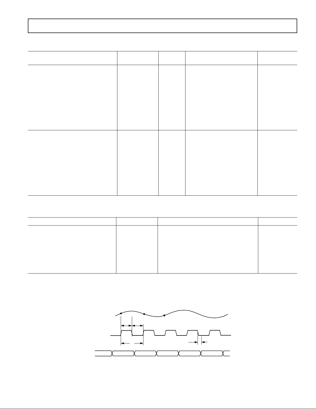
Figure 1. Timing Diagram
–3–
AD876
REFBS
REFTF
REFBF
D0
D1
D4
D5
D6
D2
D3
DV
SS
DV
DD
REFTS
D8
D9
D7
41
424347 4546
17 20191814 1615
36
35
32
31
30
34
33
44
1
2
5
6
7
3
4
373839
21 242322
40
28
27
26
29
9
10
11
8
48
13
25
12
TOP VIEW
(Not to Scale)
AD876
DRV
SSDVSS
CLK
THREE-STATE
STBY
DRV
DD
AVSSAV
DD
AIN
CML
DV
SS
PIN FUNCTION DESCRIPTIONS
SOIC TQFP
Symbol Pin No. Pin No. Type Name and Function
D0 (LSB) 3 1 DO Least Significant Bit.
D1–D4 4–7 2–5 DO Data Bits 1 through 4.
D5–D8 8–11 8–11 Data Bits 5 through 8.
D9 (MSB) 12 12 DO Most Significant Bit.
THREE- 16 23 DI
STATE
STBY 17 24 DI
CLK 15 22 DI Clock Input.
CML 26 38 AO Bypass Pin for an Internal Bias Point.
REFTF 22 30 AI Reference Top Force.
REFBF 24 34 AI Reference Bottom Force.
REFTS 21 29 AI Reference Top Sense.
REFBS 25 35 AI Reference Bottom Sense.
AIN 27 39 AI Analog Input.
AV
DD
AV
SS
DV
DD
DV
SS
DRV
DD
DRV
SS
Type: AI = Analog Input; AO = Analog Output; DI = Digital Input; DO = Digital Output; P = Power.
28 42 P +5 V Analog Supply.
1 44 P Analog Ground.
18 26 P +5 V Digital Supply.
14, 19, 20 17, 27, 28 P Digital Ground.
2 45 P +3.3 V/+5 V Digital Supply. Supply for digital
13 16 P +3.3 V/+5 V Digital Ground. Ground for digital
THREE-STATE = LOW THREE-STATE = HIGH
or N/C
Normal Operating Mode High Impedance Outputs
STBY = LOW or N/C STBY = HIGH
Normal Operating Mode Standby Mode
input and output buffers.
input and output buffers.
PIN CONFIGURATIONS
SOIC/SSOP TQFP
AV
1
SS
DRV
2
DD
3
*D0
4
*D1
5
D2
D3
6
D4
D5 REFTS
D6
D7
D8
D9 STBY
DRV
SS
DV
SS
*
PINS D0 AND D1 ARE LEFT OPEN
FOR THE AD876JR-8
AD876
7
TOP VIEW
8
(Not to Scale)
9
10
11
12
13
14
NC = NO CONNECT
28
AV
DD
AIN
27
26
CML
25
REFBS
REFBF
24
23
NC
REFTF
22
21
20
DV
SS
DV
19
SS
18
DV
DD
17
THREE-STATE
16
CLK
15
REV. B–4–
AD876
WARNING!
ESD SENSITIVE DEVICE
ABSOLUTE MAXIMUM RATINGS*
Parameter With Respect to Min Max Units
AV
DV
AV
DD
DD
SS
, DRV
DD
AV
DVSS, DRV
DVSS, DRV
AIN AV
SS
SS
–0.5 +6.5 Volts
–0.5 +6.5 Volts
SS
–0.5 +0.5 Volts
SS
–0.5 +6.5 Volts
REFTS, REFTF
REFBS, REFBF AV
Digital Inputs, CLK DV
SS
, DRV
SS
–0.5 +6.5 Volts
–0.5 +6.5 Volts
SS
Junction Temperature +150 °C
Storage Temperature –65 +150 °C
Lead Temperature
(10 sec) +300 °C
*Stresses above those listed under Absolute Maximum Ratings may cause perma-
nent damage to the device. This is a stress rating only; functional operation of the
device at these or any other conditions above those indicated in the operational
sections of this specification is not implied. Exposure to absolute maximum
ratings for extended periods may effect device reliability.
DV
DD
DRV
DV
DD
DV
SS
DRV
SS
SS
DV
DV
DD
SS
a) D0–D9 b) Three-State, Standby
ORDERING GUIDE
Temperature Package Package
Model Range Description Options
AD876JR 0°C to +70°C 28-Lead SOIC R-28
AD876JST-Reel 0°C to +70°C 48-Lead TQFP ST-48
(Tape and Reel 13")
AD876JR-8 0°C to +70°C 28-Lead SOIC R-28
AD876AR –40°C to +85°C 28-Lead SOIC R-28
AD876ARS –40°C to +85°C 28-Lead SSOP RS-28
AD876JRS 0°C to +70°C 28-Lead SSOP RS-28
AD876JRS-8 0°C to +70°C 28-Lead SSOP RS-28
DRV
DRV
DV
DD
DD
DV
SS
SS
DRV
DRV
DD
SS
c) CLK
AV
DD
REFTF
AV
AV
DD
AV
SS
d) AIN
AV
REFTS
AV
REFBS
AV
REFBF
SS
DD
INTERNAL
REFERENCE
AV
SS
DD
AV
SS
DD
AV
SS
VOLTAGE
INTERNAL
REFERENCE
VOLTAGE
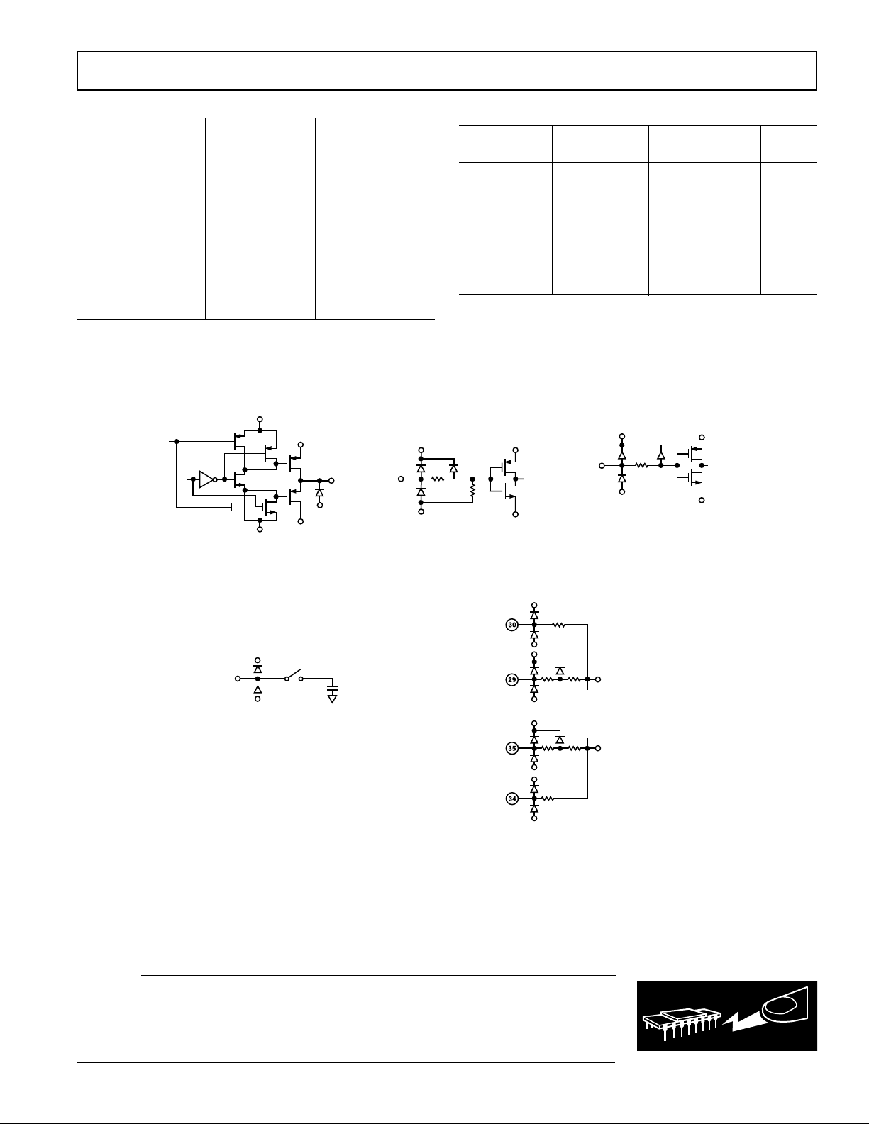
Figure 2. Equivalent Circuits
CAUTION
ESD (electrostatic discharge) sensitive device. Electrostatic charges as high as 4000 V readily
accumulate on the human body and test equipment and can discharge without detection.
Although the AD876 features proprietary ESD protection circuitry, permanent damage may
occur on devices subjected to high energy electrostatic discharges. Therefore, proper ESD
precautions are recommended to avoid performance degradation or loss of functionality.
REV. B
–5–

AD876
–Typical Perfor mance Characteristics
1
0.5
DNL – LSBs
–0.5
–1
0
2
0
–2
–4
GAIN – dB
–6
128 256 384 512 640 768 896096064 192 320 448 576 704 832
CODE OFFSET
Figure 3. AD876 Typical DNL
0
–10
–20
–30
–40
dB
–50
–60
–70
–80
–90
THD
2ND
3RD
1
FREQUENCY – MHz
10
Figure 6. THD vs. Input Frequency 2nd, 3rd Harmonics
60
55
50
45
dB
40
–8
–10
10 10001001
FREQUENCY – MHz
Figure 4. Full Power Bandwidth
60
55
50
45
dB
40
35
30
0
10
INPUT FREQUENCY – MHz
1
10
Figure 5. SINAD vs. Input Frequency
(f
= 20 MSPS, AIN = –0.5 dB)
CLK
35
30
53010 15 20 25
CLOCK FREQUENCY – MHz
Figure 7. SINAD vs. CLK Frequency (AIN = –0.5 dB)
180
170
160
150
140
mW
130
120
110
100
2
10
0255101520
CLOCK FREQUENCY – MHz
Figure 8. Power Consumption vs. Sample Rate
REV. B–6–

AD876
1
HARMONICS (dBc)
2ND –68.02
3RD –72.85
4TH –70.68
5TH –78.09
THD = –64.12
SNR = 48.73
SINAD = 48.61
SFDR = –68.02
3
6
6TH –77.74
7TH –75.62
8TH –75.98
9TH –81.20
8
5
9
2
4
7
Figure 9. AD876JR-8 Typical FFT (fIN = 3.58 MHz,
AIN = –0.5 dB, f
HARMONICS (dBc)
2ND –68.91
3RD –73.92
4TH –68.67
5TH –73.26
THD = –64.24
SNR = 55.71
SINAD = 55.14
SFDR = –68.67
3
6
= 20 MSPS)
CLOCK
6TH –80.55
7TH –82.02
8TH –81.02
9TH –88.94
8
9
1
2
5
4
7
Figure 10. AD876 Typical FFT (fIN = 3.58 MHz, AIN = –0.5 dB,
f
= 20 MSPS)
CLOCK
DEFINITIONS OF SPECIFICATIONS
INTEGRAL NONLINEARITY (INL)
Integral nonlinearity refers to the deviation of each individual
code from a line drawn from “zero” through “full scale”. The
point used as “zero” occurs 1/2 LSB before the first code transition. “Full scale” is defined as a level 1 1/2 LSB beyond the last
code transition. The deviation is measured from the center of
each particular code to the true straight line.
DIFFERENTIAL NONLINEARITY (DNL, NO MISSING
CODES)
An ideal ADC exhibits code transitions that are exactly 1 LSB
apart. DNL is the deviation from this ideal value. It is often
specified in terms of the resolution for which no missing codes
(NMC) are guaranteed.
OFFSET ERROR
The first transition should occur at a level 1/2 LSB above
“zero.” Offset is defined as the deviation of the actual first code
transition from that point.
GAIN ERROR
The first code transition should occur for an analog value 1/2 LSB
above nominal negative full scale. The last transition should
occur for an analog value 1 1/2 LSB below the nominal positive
full scale. Gain error is the deviation of the actual difference
between first and last code transitions and the ideal difference
between the first and last code transitions.
REV. B
–7–
PIPELINE DELAY (LATENCY)
The number of clock cycles between conversion initiation and
the associated output data being made available. New output
data is provided every clock cycle.
REFERENCE TOP/BOTTOM OFFSET
Resistance between the reference input and comparator input
tap points causes offset errors. These errors can be nulled out
by using the force-sense connection as shown in the Reference
Input section.
THEORY OF OPERATION
The AD876 implements a pipelined multistage architecture to
achieve high sample rate with low power. The AD876 distributes the conversion over several smaller A/D subblocks, refining
the conversion with progressively higher accuracy as it passes
the results from stage to stage. As a consequence of the distributed conversion, the AD876 requires a small fraction of the 1023
comparators used in a traditional flash type A/D. A sample-andhold function within each of the stages permits the first stage to
operate on a new input sample while the second and third stages
operate on the two preceding samples.
APPLYING THE AD876
DRIVING THE ANALOG INPUT
Figure 11 shows the equivalent analog input of the AD876, a
sample-and-hold amplifier (SHA). Bringing CLK to a logic low
level closes Switches 1 and 2 and opens Switch 3. The input
source connected to AIN must charge capacitor C
during this
H
time. When CLK transitions from logic “low” to logic “high,”
Switch 1 opens first, placing the SHA in hold mode. Switch 2
opens subsequently. Switch 3 then closes, connects the feedback loop around the op amp, and forces the output of the op
amp to equal the voltage stored on C
. When CLK transitions
H
from logic “high” to logic “low”, Switch 3 opens first. Switch 2
closes and reconnects the input to C
. Finally, Switch 1 closes
H
and places the SHA in track mode.
The structure of the input SHA places certain requirements on
the input drive source. The combination of the pin capacitance,
, and the hold capacitance, CH, is typically less than 5 pF.
C
P
The input source must be able to charge or discharge this capacitance to 10-bit accuracy in one half of a clock cycle. When
the SHA goes into track mode, the input source must charge or
discharge capacitor C
from the voltage already stored on C
H
H
(the previously captured sample) to the new voltage. In the
worst case, a full-scale voltage step on the input, the input
source must provide the charging current through the R
(50 Ω)
ON
of Switch 2 and quickly settle (within 1/2 CLK period). This
situation corresponds to driving a low input impedance. On the
other hand, when the source voltage equals the value previously
stored on C
, the hold capacitor requires no input current and
H
the equivalent input impedance is extremely high.
Adding series resistance between the output of the source and
the AIN pin reduces the drive requirements placed on the
source. Figure 12 shows this configuration. The bandwidth of
the particular application limits the size of this resistor. To
maintain the performance outlined in the data sheet specifications, the resistor should be limited to 200 Ω or less. For applications with signal bandwidths less than 10 MHz, the user may
increase the size of the series resistor proportionally. Alternatively, adding a shunt capacitance between the AIN pin and

AD876
analog ground can lower the ac source impedance. The value
of this capacitance will depend on the source resistance and the
required signal bandwidth.
The input span of the AD876 is a function of the reference
voltages. For more information regarding the input range, see
the DRIVING THE REFERENCE TERMINALS section of
the data sheet.
3
1
H
AIN
AD876
C
P
2
C
Figure 11. AD876 Equivalent Input Structure
V
S
< < 200V
AIN
Figure 12. Simple AD876 Drive Requirements
In many cases, particularly in single-supply operation, accoupling offers a convenient way of biasing the analog input
signal at the proper signal range. Figure 13 shows a typical
configuration for ac-coupling the analog input signal to the
AD876. Maintaining the specifications outlined in the data
sheet requires careful selection of the component values. The
most important concern is the f
high-pass corner that is a
-3 dB
function of R2, and the parallel combination of C1 and C2.
The f
point can be approximated by the equation
-3 dB
1
f
−3dB
=
[2×π×(R2) Ceq]
where Ceq is the parallel combination of C1 and C2. Note that
C1 is typically a large electrolytic or tantalum capacitor that
becomes inductive at high frequencies. Adding a small ceramic
or polystyrene capacitor on the order of 0.01 µF that does not
become inductive until negligibly higher frequencies maintains
a low impedance over a wide frequency range.
20 kHz. At a sample clock frequency of 20 MHz, the dc bias
current at 3 V dc is approximately 30 µA. If we choose R2 equal
to 1 kΩ and R1 equal to 50 Ω, the parallel capacitance should
be a minimum of 0.008 µF to avoid attenuating signals close to
20 kHz. Note that the bias current will cause a 31.5 mV offset
from the 3 V bias.
In systems that must use dc-coupling, use an op amp to levelshift a ground-referenced signal to comply with the input
requirements of the AD876. Figure 14 shows an AD817
configured in inverting mode with ac signal gain of –1. The dc
voltage at the noninverting input of the op amp controls the
amount of dc level shifting. A resistive voltage divider attenuates the REFBF signal. The op amp then multiplies the attenuated signal by 2. In the case where REFBF = 1.6 V, the dc
output level will be 2.6 V. The AD817 is a low cost, fast settling,
single supply op amp with a G = –1 bandwidth of 29 MHz. The
AD818 is similar to the AD817 but has a 50 MHz bandwidth.
Other appropriate op amps include the AD8011, AD812 (a dual),
and the AD8001.
Rf = 4.99kV
+V
CC
0.1mF
AD876
AIN
0Vdc
2V p-p
REFBF
RIN = 4.99kV
3kV
14.7kV
NC
AD817 OR
AD818
NC
Figure 14. Bipolar Level Shift
An integrated difference amplifier such as the AD830 is an
alternate means of providing dc level shifting. The AD830
provides a great deal of flexibility with control over offset and
gain. Figure 15 shows the AD830 precisely level-shifting a
unipolar, ground-referenced signal. The reference voltage,
REFBS, determines the amount of level-shifting. The ac gain
is 1. The AD830 offers the advantages of high CMRR, precise
gain, offset, and high-impedance inputs when compared with a
discrete implementation. For more information regarding the
AD830, see the AD830 data sheet.
AD876
V
C1
IN
C2
3V
R1
AIN
R2
I
B
V
BIAS
Figure 13. AC-Coupled Inputs
There are additional considerations when choosing the resistor
values. The ac-coupling capacitors integrate the switching
transients present at the input of the AD876 and cause a net dc
bias current, I
, to flow into the input. The magnitude of this
B
bias current increases with increasing dc signal level and also
increases with sample frequency. This bias current will result in
an offset error of (R1 + R2) × I
. If it is necessary to compen-
B
sate this error, consider making R2 negligibly small or modifying V
to account for the resultant offset.
BIAS
As an example, assume that the input to the AD876 must have
a dc bias of 3 V and the minimum expected signal frequency is
+12V
AD830
–12V
0.1
0.1
VB +2V
V
B
AD876
AIN
REFBS
2V
0
V
B
Figure 15. Level Shifting with the AD830
REFERENCE INPUT DRIVING THE REFERENCE
TERMINALS
The AD876 requires an external reference on pins REFTF and
REFBF. The AD876 provides reference sense pins, REFTS
and REFBS, to minimize voltage drops caused by external and
internal wiring resistance. A resistor ladder, nominally 250 Ω,
connects pins REFTF and REFBF.
REV. B–8–

AD876
+5V
AD876
10mF
10mF
0.1mF
10mF
0.1mF
250V (61%)
2V
NC
NC
4V
140V (61%)
250V
(615%)
REFTS
REFTF
REFBF
REFBS
NC = NO CONNECT
Figure 16 shows the equivalent input structure for the AD876
reference pins. There is approximately 5 Ω of resistance between
both the REFTF and REFBT pins and the reference ladder. If
the force-sense connections are not used, the voltage drop
across the 5 Ω resistors will result in a reduced voltage appearing across the ladder resistance. This reduces the input span of
the converter. Applying a slightly larger span between the REFTF
and REFBF pins compensates this error. Note that the temperature coefficients of the 5 Ω resistors are 1350 ppm. The
user should consider the effects of temperature when not using
a force-sense reference configuration.
REFTF
REFTS
REFBS
REFBF
5V
DACS
5V
AD876
V1
R
LADDER
250V
V2
CLK
C (VIN)
CLK
Figure 16. AD876 Equivalent Reference Structure
Do not connect the REFTS and REFBS pins in configurations
that do not use a force-sense reference. Connecting the force
and sense lines together allows current to flow in the sense lines.
Any current allowed to flow through these lines must be negligibly small. Current flow causes voltage drops across the resistance in the sense lines. Because the internal D/As of the
AD876 tap different points along the sense lines, each D/A
would receive a slightly different reference voltage if current
were flowing in these wires. To avoid this undesirable condition,
leave the sense lines unconnected. Any current allowed to flow
through these lines must be negligibly small (<100 µA).
The voltage drop across the internal resistor ladder determines
the input span of the AD876. The driving voltages required at
the V1 and V2 points are respectively +4 V and +2 V. Calculate
the full-scale input span from the equation
Input Span (V) = REFTS – REFBS
This results in a full-scale input span of approximately +2 V
when REFTS = +4 V and REFBS = +2 V In order to maintain
the requisite 2 V drop across the internal ladder, the external
reference must be capable of providing approximately 8.0 mA.
The user has flexibility in determining both the full-scale span of
the analog input and where to center this voltage. Figure 17
shows the range over which the AD876 can operate without
degrading the typical performance.
4.5
4.0
3.5
3.0
REFTF, REFTS
2.5
Figure 17. AD876 Reference Ranges
While the previous issues address the dc aspects of the AD876
reference, the user must also be aware of the dynamic imped-
(1.6, 4.5)
(1.6, 3.5)
1.0 1.5 2.0 2.5 3.0
REV. B
(2.5, 4.5)
(2.5, 3.5)
REFBF, REFBS
–9–
ance changes associated with the reference inputs. The simplified diagram of Figure 16 shows that the reference pins connect
to a capacitor for one-half of the clock period. The size of the
capacitor is a function of the analog input voltage.
The external reference must be able to maintain a low impedance over all frequencies of interest in order to provide the charge
required by the capacitance. By supplying the requisite charge,
the reference voltages will be relatively constant and performance will not degrade. For some reference configurations,
voltage transients will be present on the reference lines; this
is particularly true during the falling edge of CLK. It is important that the reference recovers from the transients and settles to
the desired level of accuracy prior to the rising edges of CLK.
There are several reference configurations suitable for the
AD876 depending on the application, desired level of accuracy,
and cost trade-offs. The simplest configuration, shown in Figure 18, utilizes a resistor string to generate the reference voltages from the converter’s analog power supply. The 0.1 µF
bypass capacitors effectively reduce high-frequency transients.
The 10 µF capacitors act to reduce the impedances at the
REFTF and REFBF pins at lower frequencies. As input frequencies approach dc, the capacitors become ineffective, and
small voltage deviations will appear across the biasing resistors.
This application can maintain 10-bit accuracy for input frequencies above approximately 200 Hz. 8-bit applications can use this
circuit for input frequencies above approximately 50 Hz.
Figure 18. Low Cost Reference Circuit
This reference configuration provides the lowest cost but has
several disadvantages. These disadvantages include poor dc
power supply rejection and poor accuracy due to the variability
of the internal and external resistors.
The AD876 offers force-sense reference connections to eliminate the voltage drops associated with the internal connections
to the reference ladder. Figure 19 shows a suggested circuit
using an AD826 dual, high speed op amp. This configuration
uses 3.6 V and 1.6 V reference voltages for REFT and REFB,
respectively. The connections shown in Figure 19 configure the
op amps as voltage followers.

AD876
C3
0.1mF
AD876
REFTS
REFTF
REFBS
REFBF
REFT
REFB
6
2
1/2
AD826
+5V
5
3
8
7
1/2
AD826
6
4
0.1mF
0.1mF
C4
C5
C1
0.1mF
0.1mF
C2
Figure 19. Kelvin Connected Reference Using the AD826
By connecting the op amp feedback through the sense connections of the AD876, the outputs of the op amps automatically
adjust to compensate for the voltage drops that occur within
the converter. The AD826 has the advantage of being able to
maintain stability while driving unlimited capacitive loads. As a
result, 0.1 µF capacitors C1, C2, and C3 can connect directly
to the outputs of the op amps. These decoupling capacitors
reduce high frequency transients. Capacitors C4 and C5 shunt
across the internal resistors of the force sense connections and
prevent instability.
This configuration provides excellent performance and a minimal number of components. The circuit also offers the advantage of operating from a single +5 V supply. While alternative
op amps may also be suitable, consider the stability of these op
amps while driving capacitive loads.
The circuit shown in Figure 20 allows a wider selection of op
amps when compared with the previous configuration. An
AD876
REFTS
REFTF
REFBS
REFBF
REFT
REFB
47nF
1/2
OP-295
47nF
1/2
OP-295
20kV
10V
10mF 0.1mF
20kV
10V
10mF
22mF
0.1mF
common ground, are effectively removed by the AD876’s high
common-mode rejection.
High frequency noise sources, V
and VN2, are shunted to
N1
ground by decoupling capacitors. Any voltage drops between
the analog input ground and the reference bypassing points will
be treated as input signals by the converter via the reference
inputs. Consequently, the reference decoupling capacitors
should be connected to the same analog ground point used to
define the analog input voltage. (For further suggestions, see
the “Grounding and Layout Rules” section of the data sheet.)
V
4V
N1
V
2V
N2
REFTF
REFBF
AD876
AIN
Figure 21. Recommended Bypassing for the Reference
Inputs
CLOCK INPUT
The AD876 clock input is buffered internally with an inverter
powered from the DRV
pin. This feature allows the AD876
DD
to accommodate either +5 V or +3.3 V CMOS logic input signal swings with the input threshold for the CLK pin nominally
at DRV
DD
/2.
The AD876’s pipelined architecture operates on both rising and
falling edges of the input clock. To minimize duty cycle variations the recommended logic family to drive the clock input is
high speed or advanced CMOS (HC/HCT, AC/ACT) logic.
CMOS logic provides both symmetrical voltage threshold levels
and sufficient rise and fall times to support 20 MSPS operation.
The AD876 is designed to support a conversion rate of 20 MSPS;
running the part at slightly faster clock rates may be possible,
although at reduced performance levels. Conversely, some
slight performance improvements might be realized by clocking
the AD876 at slower clock rates.
The power dissipated by the correction logic and output buffers
is largely proportional to the clock frequency; running at reduced
clock rates provides a reduction in power consumption. Figure
8 illustrates this trade-off.
Figure 20. Kelvin Connected Reference Using the OP295
OP295 dual, single-supply op amp provides stable 3.6 V and
1.6 V reference voltages. The AD822 dual op amp is also suitable for single-supply applications. Each half of the OP295 is
compensated to drive the 10 µF and 0.1 µF decoupling capaci-
tors at the REFTF and REFBF pins and maintain stability.
Like any high resolution converter, the layout and decoupling of
the reference is critical. The actual voltage digitized by the
AD876 is relative to the reference voltages. In Figure 21, for
example, the reference return and the bypass capacitors are
connected to the shield of the incoming analog signal. Disturbances in the ground of the analog input, that will be commonmode to the REFT, REFB, and AIN pins because of the
DIGITAL INPUTS AND OUTPUTS
Each of the AD876 digital control inputs, THREE-STATE and
STBY, has an input buffer powered from the DRV
pins. With DRV
set to +5 V, all digital inputs readily inter-
DD
supply
DD
face with +5 V CMOS logic. For interfacing with lower voltage
CMOS logic, DRV
can be set to 3.3 V, effectively lowering
DD
the nominal input threshold of all digital inputs to 3.3 V/2 =
1.65 V.
The format of the digital output is straight binary. Table I shows
the output format for the case where REFTS = 4 V and REFBS
= 2 V.
REV. B–10–

AD876
THREE-STATE
ACTIVE
HIGH IMPEDANCE
D0–D9
t
DD
t
HL
Table I. Output Data Format
Approx. THREE- DATA
AIN (V) STATE D9 D8 D7 D6 D5 D4 D3 D2 D1 D0
>4 0 1111111111
4 0 1111111111
3 0 1000000000
2 0 0000000000
<2 0 0000000000
X 1 ZZZZZZZZZZ
A low power mode feature is provided such that for STBY =
HIGH and the clock disabled, the static power of the AD876
will drop below 50 mW.
GROUNDING AND LAYOUT RULES
As is the case for any high performance device, proper grounding and layout techniques are essential in achieving optimal
performance. The analog and digital grounds on the AD876
have been separated to optimize the management of return
currents in a system. It is recommended that a printed circuit
board (PCB) of at least 4 layers employing a ground plane and
power planes be used with the AD876. The use of ground and
power planes offers distinct advantages:
1. The minimization of the loop area encompassed by a signal
and its return path.
2. The minimization of the impedance associated with ground
and power paths.
3. The inherent distributed capacitor formed by the power
plane, PCB insulation, and ground plane.
These characteristics result in both a reduction of electromagnetic interference (EMI) and an overall improvement in
performance.
It is important to design a layout which prevents noise from
coupling onto the input signal. Digital signals should not be run
in parallel with the input signal traces and should be routed
away from the input circuitry. Separate analog and digital
grounds should be joined together directly under the AD876. A
solid ground plane under the AD876 is also acceptable if the
power and ground return currents are managed carefully. A
general rule of thumb for mixed signal layouts dictates that the
return currents from digital circuitry should not pass through
critical analog circuitry. For further layout suggestions, see the
AD876 Evaluation Board data sheet.
For DRVDD = 5 V, the AD876 output signal swing is compatible with both high speed CMOS and TTL logic families. For
TTL, the AD876 on-chip, output drivers were designed to
support several of the high speed TTL families (F, AS, S). For
applications where the clock rate is below 20 MSPS, other TTL
families may be appropriate. For interfacing with lower voltage
CMOS logic, the AD876 sustains 20 MSPS operation with
DRV
= 3.3 V. In all cases, check your logic family data
DD
sheets for compatibility with the AD876 Digital Specification
table.
THREE-STATE OUTPUTS
The digital outputs of the AD876 can be placed in a high impedance state by setting the THREE-STATE pin to HIGH.
This feature is provided to facilitate in-circuit testing or
evaluation. Note that this function is not intended for enabling/
disabling the ADC outputs from a bus at 20 MSPS. Also, to
avoid corruption of the sampled analog signal during conversion
(3.5 clock cycles), it is highly recommended that the AD876
outputs be enabled on the bus prior to the first sampling. For
the purpose of budgetary timing, the maximum access and float
delay times (t
, tHL shown in Figure 15) for the AD876 are
DD
150 ns.
Figure 22. High-Impedance Output Timing Diagram
DIGITAL OUTPUTS
Each of the on-chip buffers for the AD876 output bits (D0–D9)
is powered from the DRV
. The output drivers are sized to handle a variety of logic
DV
DD
supply pins, separate from AVDD or
DD
families while minimizing the amount of glitch energy generated. In all cases, a fan-out of one is recommended to keep the
capacitive load on the output data bits below the specified 20 pF
level.
REV. B
–11–

AD876
REFTS
REFTF
REFBF
REFBS
+5VD
JP4
VP8
DC_IN
REFTF
VP1
C50
10mF
+
0.1mF
R14
100V
C62
R16
1kV
+5VD
REFTS
VP3
VP4
REFBS
10mF
+
REFBF
VP2
C4
R17
1.13kV
R18
1kV
JP1
JP2
STBY
VP6
3ST
VP5
TP3
C64
0.1mF
C56
0.1mF
C2
10mF
+
74F04
4
+5VA
U4
15
16
17
18
19
20
21
22
23
24
25
26
27
28
3
AD876
CLK
3_STATE
STBY
DV
DD
SUBST
NC
REFTS
REFTF
NC
REFBF
REFBS
CML
AIN
AV
DD
U1
DV
DRV
DRV
AV
1
DB9
DB8
DB7
DB6
DB5
DB4
DB3
DB2
DB1
DB0
U4
74F04
SS
SS
DD
SS
TP4
2
CLK_IN
TP1
R1
51V
U2
74ALS541
5
6
7
8
9
0
1
2
3
4
1
G1
19
G2
9
A7
8
A6
7
A5
6
A4
A3
5
A2
4
A1
3
A0
2
1
G1
19
G2
9
A7
8
A6
7
A5
A4
6
A3
5
A2
4
A1
3
A0
2
74ALS541
11
Y7
12
Y6
13
Y5
14
D5
Y4
15
D6
Y3
16
Y2
D7
Y1
17
D8
Y0
18
D9
U3
11
Y7
12
Y6
13
Y5
14
D0
Y4
15
Y3
D1
16
Y2
D2
Y1
17
D3
Y0
18
D4
14
13
9
12
11
8
10
7
6
9
8
5
4
7
6
3
5
2
4
1
3
0
2
1
J1
P1 1
*
*
*
R12*
P1 3
P1 5
P1 7
P1 9
P1 11
P1 13
P1 15
P1 17
P1 19
P1 21
P1 23
P1 25
P1 27
P1 29
P1 31
P1 33
P1 35
P1 37
P1 39
D9
R2
D8
R3*
D7
R4*
D6
R5*
D5
R6*
D4
R7*
D3
R8
D2
R9*
D1
R10*
D0
R11
P1 2
P1 4
P1 6
P1 8
P1 10
P1 12
P1 14
P1 16
P1 18
P1 20
P1 22
P1 24
P1 26
P1 28
P1 30
P1 32
P1 34
P1 36
P1 38
P1 40
+
+5VD
C49
10mF
C54
0.1mF
*R2–R12 = 20V
TP2
AIN
231INT_CM
EXT_CM
JP5
TP18
J2
R15
51V
C1
0.1mF
C3
47mF
+
Figure 23. AD876 Evaluation Board Schematic
REV. B–12–

AD876
Figure 24. Silkscreen Layer, Component Side PCXB Layout
REV. B
Figure 25. Silkscreen Layer, Circuit Side PCB Layout
–13–

AD876
Figure 26. Component Side PCB Layout
Figure 27. Circuit Side PCB Layout
REV. B–14–

AD876
Figure 28. Ground Layer PCB Layout
REV. B
Figure 29. Power Layer PCB Layout
–15–

AD876
OUTLINE DIMENSIONS
Dimensions shown in inches and (mm).
R-28
28-Lead Wide Body (SOIC)
0.7125 (18.10)
0.6969 (17.70)
28 15
141
0.2992 (7.60)
0.2914 (7.40)
0.4193 (10.65)
0.3937 (10.00)
PIN 1
0.0118 (0.30)
0.0040 (0.10)
28-Lead Plastic Thin Quad Flatpack (TQFP)
0.059 +0.008 –0.004
(1.50 +0.2 –0.1)
0.02 ± 0.008
(0.5 ± 0.2)
SEATING
PLANE
0.004 ± 0.002
(0.1 ± 0.05)
(3.5
° ± 3.5°)
0.005 +0.002 –0.0008
(0.127 +0.05 –0.02)
0.0500
(1.27)
BSC
0.0192 (0.49)
0.0138 (0.35)
0.055 ± 0.002
(1.40 ± 0.05)
0
° MIN
0.1043 (2.65)
0.0926 (2.35)
SEATING
PLANE
0.0125 (0.32)
0.0091 (0.23)
ST-48
0.354 ± 0.008 (9.00 ± 0.2) SQ
36
37
TOP VIEW
(PINS DOWN)
48
1
0.02 ± 0.003
(0.50 ± 0.08)
0.007 +0.003 –0.001
(0.18 +0.08 –0.03)
0.0291 (0.74)
0.0098 (0.25)
0.0500 (1.27)
8°
0°
0.0157 (0.40)
25
24
13
12
x 45°
0.039 (1.00)
REF
0.276 ± 0.004
(7.0 ± 0.1)
SQ
RS-28
28-Lead Shrink Small Outline Package (SSOP)
0.407 (10.34)
0.397 (10.08)
28 15
0.311 (7.9)
0.301 (7.64)
0.078 (1.98)
0.068 (1.73)
0.008 (0.203)
0.002 (0.050)
PIN 1
0.0256
(0.65)
BSC
0.015 (0.38)
0.010 (0.25)
SEATING
PLANE
0.212 (5.38)
141
0.07 (1.79)
0.066 (1.67)
0.009 (0.229)
0.005 (0.127)
0.205 (5.21)
8°
0°
PRINTED IN U.S.A. C1991a–0–1/98
0.03 (0.762)
0.022 (0.558)
REV. B–16–
 Loading...