

PRELIMINARY TECHNICAL DATA
Precision Very Low Noise
PPrreelliimmiinnaarry
y Technical Data
AD8671/AD8672/AD8674
FEATURES
Low Noise: 3nV/√Hz
Wide Bandwidth: 10MHz
Low Input Bias Current: 10nA max.
Low Offset Voltage: 75 µV max.
High open loop gain: 135dB
Low Supply Current: 3 mA/Amp
Dual supply operation: ±5V to ±15V
Unity Gain Stable
No Phase Reversal
APPLICATIONS
PLL filters
Instrumentation
Sensors and Controls
Professional quality audio
GENERAL DESCRIPTION
The AD8671, AD8672 and AD8674 are precision
single, dual and quad amplifiers featuring very low
noise, very low offset voltage and drift, low input bias
current, 10Mhz bandwidth and low power
consumption. Outputs are stable with capacitive loads
of over 100pF. Supply current is less than 3 mA per
amplifier at 30V.
Applications for these amplifiers include high quality
PLL filters, instrumentation--thermocouple, RTD,
strain-bridge and other sensor signal conditioning-precision filters and professional quality audio.
The AD8671, AD8672 and AD8674 are specified
over the extended industrial (-40° to +125°C)
temperature range. The AD8671, single, is available
in the 8-lead MSOP and 8-lead SOIC packages.
The AD8672, dual, is available in the 8-lead MSOP
and 8-lead SOIC packages. The AD8674, quad, is
Information furnished by Analog Devices is believed to be accurate and
reliable. However, no responsibility is assumed by Analog Devices for its
use, nor for any infringements of patents or other rights of third parties
which may result from its use. No license is granted by implication or
otherwise under any patent or patent rights of Analog Devices.
AD8671/AD8672/AD8674 Rev 0.2 2/21/02
available in 14-lead TSSOP and narrow 14-lead SO
packages. Surface mount devices in TSSOP and
MSOP packages are available in tape and reel only.
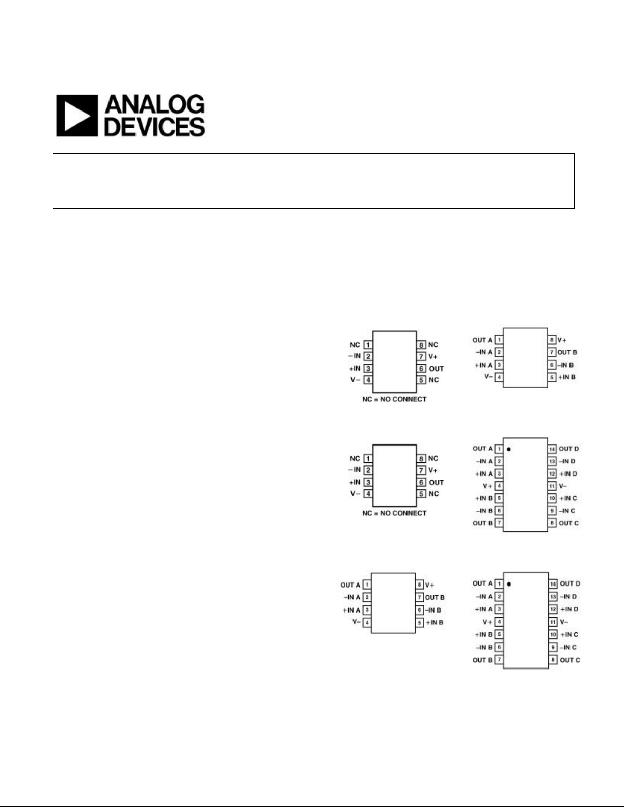
PIN CONFIGURATIONS
8-Lead MSOP
(RM-8)
AD8671
8-Lead SO
(R-8)
AD8672
8-Lead SO
(R-8)
AD8671
14-Lead TSSOP
(RU-14)
AD8674
8-Lead MSOP
(RM-8)
AD8672
One Technology Way, PO Box 9106, Norwood, MA 02062-9106,
USA
Tel: 781/329-4700 www.analog.com
Fax: 781/326-8703 © Analog Devices, Inc., 1997
14-Lead SO
(R-14)
AD8674

PRELIMINARY TECHNICAL DATA
Preliminary Technical Data AD8671/AD8672/AD8674
ELECTRICAL CHARACTERISTICS (@ V
Parameter Symbol Conditions Min Typ Max Units
INPUT CHARACTERISTICS
Offset Voltage VOS 75 µV
-40°< TA < +125°C 175 µV
Input Bias Current IB -10 10 nA
Input Offset Current IOS -10 10 nA
Input Voltage Range -2.5 2.5 V
Common-Mode Rejection Ratio CMRR VCM = -2V to 2V 100 130 dB
Large Signal Voltage Gain AVO RL = 2 kΩ , Vo= -3V to 3V 1000 6000 V/mV
Offset Voltage Drift ∆VOS/∆T -40°< TA < +125°C 0.3 1 µV/°C
OUTPUT CHARACTERISTICS
Output Voltage High VOH IL = 1 mA, -40°C to +125°C 3 3.8 V
Output Voltage Low VOL IL = 1 mA, -40°C to +125°C -3.9 -3 V
Output Current I
POWER SUPPLY
Power Supply Rejection Ratio PSRR VS = ±2.5 V to ±15 V 110 130 dB
Supply Current/Amplifier ISY VO = 0V 3000 3500 µA
-40°<TA < +125°C 4000 µA
DYNAMIC PERFORMANCE
Slew Rate SR RL =2 kΩ 4 V/µs
Gain Bandwidth Product GBP 10 MHz
NOISE PERFORMANCE
Voltage Noise e
Voltage Noise Density e
Current Noise Density i
±10 mA
OUT
n p-p 0.1 Hz to 10 Hz 0.08
n f = 1 kHz 3
n f = 1 kHz 0.2
= ±5.0V, VCM = 0V, TA=+25°C unless noted
S
µV p-p
nV/√Hz
pA/√Hz
AD8671/AD8672/AD8674 Rev0.2 2/21/02

PRELIMINARY TECHNICAL DATA
Preliminary Technical Data AD8671/AD8672/AD8674
ELECTRICAL CHARACTERISTICS (@ V
Parameter Symbol Conditions Min Typ Max Units
INPUT CHARACTERISTICS
Offset Voltage VOS 75 µV
-40°< TA < +125°C 175 µV
Input Bias Current IB -10 10 nA
Input Offset Current IOS -10 10 nA
Input Voltage Range -12.5 12.5 V
Common-Mode Rejection Ratio CMRR VCM = -12V to 12V 110 140 dB
Large Signal Voltage Gain AVO RL = 2 kΩ , Vo = -10V to 10V 1000 6000 V/mV
Offset Voltage Drift ∆VOS/∆T -40°< TA < +125°C 0.3 1 µV/°C
OUTPUT CHARACTERISTICS
Output Voltage High VOH IL = 10 mA, -40°C to +125°C -10 13.5 V
Output Voltage Low VOL IL = 10 mA, -40°C to +125°C -13.5 10 V
Output Current I
Short Circuit Current I
POWER SUPPLY
Power Supply Rejection Ratio PSRR VS = ±2.5 V to ±15 V 110 130 dB
Supply Current/Amplifier ISY VO = 0V 3000 3500 µA
-40°<TA < +125°C 4000 µA
DYNAMIC PERFORMANCE
Slew Rate SR RL =2 kΩ 4 V/µs
Gain Bandwidth Product GBP 10 MHz
NOISE PERFORMANCE
Voltage Noise e
Voltage Noise Density e
Current Noise Density i
±20 mA
OUT
SC
n p-p 0.1 Hz to 10 Hz 0.08
n f = 1 kHz 3
n f = 1 kHz 0.2
= ±15V, VCM = 0V, TA=+25°C unless noted)
S
±30 mA
µV p-p
nV/√Hz
pA/√Hz
AD8671/AD8672/AD8674 Rev0.2 2/21/02

PRELIMINARY TECHNICAL DATA
Preliminary Technical Data AD8671/AD8672/AD8674
ABSOLUTE MAXIMUM RATINGS
Supply voltage ............................................................................36V
Input Voltage....................................................................Vs- to Vs+
Differential Input Voltage .........................................................TBD
Output Short-Circuit Duration..........................................Indefinite
Storage Temperature Range
RM, R, RU Package.......................................-65°C to +150°C
Operating Temperature Range
AD8671/AD8672/AD8674............................-40°C to +125°C
Junction Temperature Range
RM, R, RU Package.......................................-65°C to +150°C
Lead Temperature Range (Soldering, 60 Sec)........................+300°C
Model Temperature Range Package Description Package Option
AD8671ARM -40°C to +125°C 8-Pin MSOP RM -8
AD8671AR -40°C to +125°C 8-Pin SOIC R-8
AD8672ARM -40°C to +125°C 8-Pin MSOP RM -8
AD8672AR -40°C to +125°C 8-Pin SOIC R-8
AD8674ARU -40°C to +125°C 14-Pin TSSOP RU-14
AD8674AR -40°C to +125°C 14-Pin SOIC R-14
1
Package Type θJA θ
8-pin MSOP (RM) 190 44 °C/W
8-Pin SOIC (R) 158 43 °C/W
14-Pin TSSOP (RU) 180 35 °C/W
14-Pin SOIC (R) 120 36 °C/W
NOTES
1
Absolute maximum ratings apply at 25°C, unless otherwise noted.
2
θJA is specified for the worst case conditions, i.e., θJAis specified for device soldered
in circuit board for surface mount packages.
JC Units
ORDERING GUIDE
AD8671/AD8672/AD8674 Rev0.2 2/21/02
 Loading...