

Precision, Very Low Noise, Low Input
–
+
–
+
FEATURES
Very low noise: 2.8 nV/√Hz, 77 nV p-p
Wide bandwidth: 10 MHz
Low input bias current: 12 nA max
Low offset voltage: 75 μV max
High open-loop gain: 120 dB min
Low supply current: 3 mA typ per amplifier
Dual-supply operation: ±5 V to ±15 V
Unity-gain stable
No phase reversal
APPLICATIONS
PLL filters
Filters for GPS
Instrumentation
Sensors and controls
Professional quality audio
GENERAL DESCRIPTION
The AD8671/AD8672/AD8674 are very high precision amplifiers
featuring very low noise, very low offset voltage and drift, low
input bias current, 10 MHz bandwidth, and low power
consumption. Outputs are stable with capacitive loads of over
1000 pF. Supply current is less than 3 mA per amplifier at 30 V.
The AD8671/AD8672/AD8674’s combination of ultralow noise,
high precision, speed, and stability is unmatched. The MSOP
version of the AD8671/AD8672 requires only half the board
space of comparable amplifiers.
Applications for these amplifiers include high quality PLL
filters, precision filters, medical and analytical instrumentation,
precision power supply controls, ATE, data acquisition, and
precision controls as well as professional quality audio.
The AD8671/AD8672 are specified over the extended industrial
temperature range (−40°C to +125°C), and the AD8674 is specified
over the industrial temperature range (−40°C to +85°C).
Bias Current Operational Amplifiers
AD8671/AD8672/AD8674
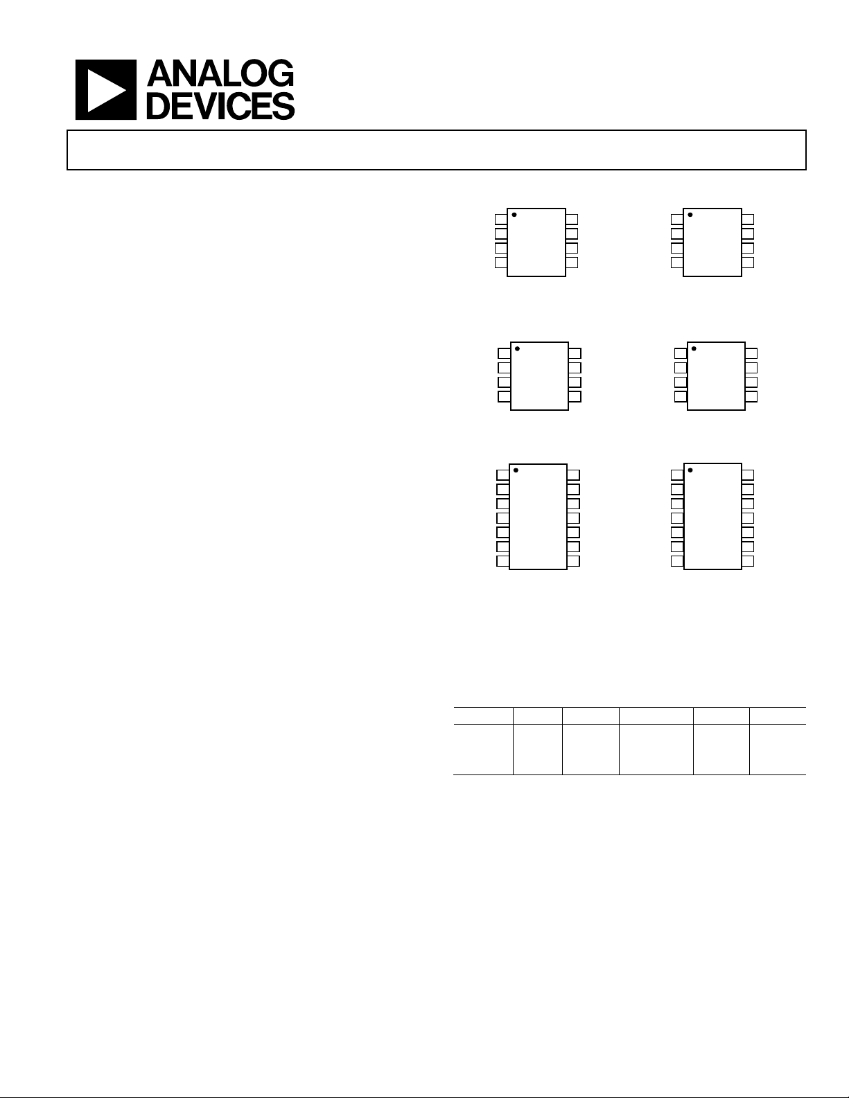
PIN CONFIGURATIONS
NC
1
AD8671
2
IN
TOP VIEW
IN
3
(Not to Scale)
V–
4
NC = NO CONNECT
Figure 1. 8-Lead SOIC_N (R-8)
OUT A
1
AD8672
2
–IN A
+IN A
V–
TOP VIEW
3
(Not to Scale)
4
Figure 3. 8-Lead SOIC-N (R-8)
OUT A
1
–IN A
2
3
+IN A
+IN B
–IN B
OUT B
V+
AD8674
4
TOP VIEW
(Not to Scale)
5
6
7
Figure 5. 14-Lead SOIC_N (R-14)
The AD8671, AD8672, and AD8674 are members of a growing
series of low noise op amps offered by Analog Devices, Inc.
Table 1. Voltage Noise
Package 0.9 nV 1.1 nV 1.8 nV 2.8 nV 3.8 nV
Single AD797 AD8597 ADA4004-1 AD8675 AD8671
Dual AD8599 ADA4004-2 AD8676 AD8672
Quad ADA4004-4 AD8674
NC
8
7
V+
OUT
6
NC
5
03718-B-001
NC
1
AD8671
2
IN
TOP VIEW
IN
3
(Not to Scale)
V–
4
NC = NO CONNECT
NC
8
7
V+
OUT
6
NC
5
03718-B-002
Figure 2. 8-Lead MSOP (RM-8)
8
7
6
5
V+
OUT B
–IN B
+IN B
1
V–
AD8672
2
TOP VIEW
3
(Not to Scale)
4
–IN A
+IN A
03718-B-003
8
7
6
5
V+
OUT B
–IN B
+IN B
03718-B-004
OUT A
Figure 4. 8-Lead MSOP (RM-8)
14
13
12
11
10
9
8
OUT D
–IN D
+IN D
V–
+IN C
–IN C
OUT C
1
–IN A
2
+IN A
3
AD8674
V+
4
TOP VIEW
(Not to Scale)
+IN B
5
–IN B
6
OUT B
03718-B-005
7
14
13
12
11
10
9
8
OUT D
–IN D
+IN D
V–
+IN C
–IN C
OUT C
03718-B-006
OUT A
Figure 6. 14-Lead TSSOP (RU-14)
The AD8671/AD8672 are available in the 8-lead SOIC and
8-lead MSOP packages. The AD8674 is available in 14-lead
SOIC and 14-lead TSSOP packages.
Surface-mount devices in MSOP packages are available in tape
and reel only.
Rev. E
Information furnished by Analog Devices is believed to be accurate and reliable.
However, no responsibility is assumed by Analog Devices for its use, nor for any
infringements of patents or other rights of third parties that may result from its use.
Specifications subject to change without notice. No license is granted by implication
or otherwise under any patent or patent rights of Analog Devices. Trademarks and
registered trademarks are the property of their respective owners.
One Technology Way, P.O. Box 9106, Norwood, MA 02062-9106, U.S.A.
Tel: 781.329.4700 www.analog.com
Fax: 781.461.3113 ©2004–2010 Analog Devices, Inc. All rights reserved.

AD8671/AD8672/AD8674
TABLE OF CONTENTS
Specifications ..................................................................................... 3
Output Phase Reversal ............................................................... 12
Electrical Characteristics, ±5.0 V ............................................... 3
Electrical Characteristics, ±15 V ................................................ 4
Absolute Maximum Ratings ............................................................ 5
ESD Caution .................................................................................. 5
Typical Performance Characteristics ............................................. 6
Applications ..................................................................................... 11
Power Dissipation Calculations ................................................ 11
Unity-Gain Follower Applications ........................................... 11
REVISION HISTORY
6/10—Rev. D to Rev. E
Added Table 1 and Preceding Sentence ..................................... 1
12/09—Rev. C to Rev. D
Changes to Features and General Description Sections .......... 1
Changes to Absolute Maximum Ratings Section, Table 3,
and Table 4 ................................................................................ 5
Added Power Dissipation Calculations Section ..................... 11
Updated Outline Dimensions ................................................... 15
Changes to Ordering Guide ...................................................... 17
6/05—Rev. B to Rev. C
Total Noise vs. Source Resistance ............................................. 12
Total Harmonic Distortion (THD) and Noise ....................... 13
Driving Capacitive Loads .......................................................... 13
GPS Receiver ............................................................................... 14
Band-Pass Filter .......................................................................... 14
PLL Synthesizers and Loop Filters ........................................... 14
Outline Dimensions ....................................................................... 15
Ordering Guide .......................................................................... 17
4/04—Rev. A to Rev. B
Changes to Figure 32 .................................................................. 11
Changes to Figures 36, 37, and 38 ............................................ 12
1/04—Rev. 0 to Rev. A
Added AD8672 and AD8674 parts .............................. Universal
Changes to Specifications ............................................................. 3
Deleted Figure 3 ............................................................................. 6
Changes to Figures 7, 8, and 9 ..................................................... 6
Changes to Figure 37 .................................................................. 12
Added new Figure 32 ................................................................. 10
Changes to Figure 6 ...................................................................... 1
Updated Outline Dimensions ................................................... 14
Changes to Ordering Guide ...................................................... 16
Rev. E | Page 2 of 20

AD8671/AD8672/AD8674
SPECIFICATIONS
ELECTRICAL CHARACTERISTICS, ±5.0 V
VS = ±5.0 V, VCM = 0 V, TA = 25°C, unless otherwise noted.
Table 2.
Parameter Symbol Conditions Min Typ Max Unit
INPUT CHARACTERISTICS
Offset Voltage VOS 20 75 μV
–40°C < TA < +125°C 30 125 μV
Offset Voltage Drift ∆VOS/∆T –40°C < TA < +125°C
AD8671 0.3 0.5 μV/°C
AD8672/AD8674 0.3 0.8 μV/°C
Input Bias Current IB –12 +3 +12 nA
+25°C < TA < +125°C –20 +5 +20 nA
–40°C < TA < +125°C –40 +8 +40 nA
Input Offset Current IOS –12 +6 +12 nA
+25°C < TA < +125°C –20 +6 +20 nA
–40°C < TA < +125°C –40 +8 +40 nA
Input Voltage Range –2.5 +2.5 V
Common-Mode Rejection Ratio CMRR VCM = –2.5 V to +2.5 V 100 120 dB
Large Signal Voltage Gain AVO R
Input Capacitance, Common Mode C
Input Capacitance, Differential Mode C
6.25 pF
INCM
7.5 pF
INDM
Input Resistance, Common Mode RIN 3.5 GΩ
Input Resistance, Differential Mode R
15 MΩ
INDM
OUTPUT CHARACTERISTICS
Output Voltage High VOH R
Output Voltage Low VOL R
Output Voltage High VOH R
Output Voltage Low VOL R
Output Current I
±10 mA
OUT
POWER SUPPLY
Power Supply Rejection Ratio PSRR VS = ±4 V to ±18 V
AD8671/AD8672 110 130 dB
AD8674 106 115 dB
Supply Current/Amplifier ISY V
–40°C < TA < +125°C 4.2 mA
DYNAMIC PERFORMANCE
Slew Rate SR RL = 2 kΩ 4 V/μs
Settling Time tS To 0.1% (4 V step, G = 1) 1.4 μs
To 0.01% (4 V step, G = 1) 5.1 μs
Gain Bandwidth Product GBP 10 MHz
NOISE PERFORMANCE
Peak-to-Peak Noise e
0.1 Hz to 10 Hz 77 100 nV p-p
n p-p
Voltage Noise Density en f = 1 kHz 2.8 3.8 nV/√Hz
Current Noise Density in f = 1 kHz 0.3 pA/√Hz
Channel Separation
AD8672/AD8674 CS f = 1 kHz –130 dB
f = 10 kHz –105 dB
= 2 kΩ, VO = –3 V to +3 V 1000 6000 V/mV
L
= 2 kΩ, –40°C to +125°C +3.8 +4.0 V
L
= 2 kΩ, –40°C to +125°C –3.9 –3.8 V
L
= 600 Ω +3.7 +3.9 V
L
= 600 Ω –3.8 –3.7 V
L
= 0 V 3 3.5 mA
O
Rev. E | Page 3 of 20

AD8671/AD8672/AD8674
ELECTRICAL CHARACTERISTICS, ±15 V
VS = ±15 V, VCM = 0 V, TA = 25°C, unless otherwise noted.
Table 3.
Parameter Symbol Conditions Min Typ Max Unit
INPUT CHARACTERISTICS
Offset Voltage VOS 20 75 μV
–40°C < TA < +125°C 30 125 μV
Offset Voltage Drift ∆VOS/∆T –40°C < TA < +125°C
AD8671 0.3 0.5 μV/°C
AD8672/AD8674 0.3 0.8 μV/°C
Input Bias Current IB –12 +3 +12 nA
+25°C < TA < +125°C –20 +5 +20 nA
–40°C < TA < +125°C –40 +8 +40 nA
Input Offset Current IOS –12 +6 +12 nA
+25°C < TA < +125°C –20 +6 +20 nA
–40°C < TA < +125°C –40 +8 +40 nA
Input Voltage Range –12 +12 V
Common-Mode Rejection Ratio CMRR VCM = –12 V to +12 V 100 120 dB
Large Signal Voltage Gain AVO R
Input Capacitance, Common Mode C
Input Capacitance, Differential Mode C
6.25 pF
INCM
7.5 pF
INDM
Input Resistance, Common Mode RIN 3.5 GΩ
Input Resistance, Differential Mode R
15 MΩ
INDM
OUTPUT CHARACTERISTICS
Output Voltage High VOH R
Output Voltage Low VOL R
Output Voltage High VOH R
Output Voltage Low VOL R
Output Current I
±20 mA
OUT
Short Circuit Current ISC ±30 mA
POWER SUPPLY
Power Supply Rejection Ratio PSRR VS = ±4 V to ±18 V
AD8671/AD8672 110 130 dB
AD8674 106 115 dB
Supply Current/Amplifier ISY V
–40°C <TA < +125°C 4.2 mA
DYNAMIC PERFORMANCE
Slew Rate SR RL = 2 kΩ 4 V/μs
Settling Time tS To 0.1% (10 V step, G = 1) 2.2 μs
To 0.01% (10 V step, G = 1) 6.3 μs
Gain Bandwidth Product GBP 10 MHz
NOISE PERFORMANCE
Peak-to-Peak Noise e
0.1 Hz to 10 Hz 77 100 nV p-p
n p-p
Voltage Noise Density en f = 1 kHz 2.8 3.8 nV/√Hz
Current Noise Density in f = 1 kHz 0.3 pA/√Hz
Channel Separation
AD8672/AD8674 CS f = 1 kHz –130 dB
f = 10 kHz –105 dB
= 2 kΩ, VO = –10 V to +10 V 1000 6000 V/mV
L
= 2 kΩ, –40°C to +125°C +13.2 +13.8 V
L
= 2 kΩ, –40°C to +125°C –13.8 –13.2 V
L
= 600 Ω +11 +12.3 V
L
= 600 Ω –12.4 –11 V
L
= 0 V 3 3.5 mA
O
Rev. E | Page 4 of 20
AD8671/AD8672/AD8674
ABSOLUTE MAXIMUM RATINGS
Table 4.1
Parameter Rating
Supply Voltage 36 V
Input Voltage VS– to VS+
Differential Input Voltage ±0.7 V
Output Short-Circuit Duration Indefinite
Storage Temperature Range
All Packages –65°C to +150°C
Operating Temperature Range
8-Lead Packages –40°C to +125°C
14-Lead Packages –40°C to +85°C
Junction Temperature Range
All Packages –65°C to +150°C
Lead Temperature Range (Soldering, 60 sec) 300°C
1
Absolute maximum ratings apply at 25°C, unless otherwise noted.
Stresses above those listed under Absolute Maximum Ratings
may cause permanent damage to the device. This is a stress
rating only; functional operation of the device at these or any
other conditions above those indicated in the operational
section of this specification is not implied. Exposure to absolute
maximum rating conditions for extended periods may affect
device reliability.
See the Applications section for a related discussion on power.
Table 5. Package Characteristics
Package Type θ
1
θ
JA
Unit
JC
8-Lead MSOP (RM) 142 44 °C/W
8-Lead SOIC_N (R) 120 43 °C/W
14-Lead SOIC_N (R) 90 36 °C/W
14-Lead TSSOP (RU) 112 35 °C/W
1
θJA is specified for the worst-case conditions, that is., θJA is specified for the
device soldered on a 4-layer circuit board for surface-mount packages.
ESD CAUTION
ESD (electrostatic discharge) sensitive device. Electrostatic charges as high as 4000 V readily accumulate on
the human body and test equipment and can discharge without detection. Although this product features
proprietary ESD protection circuitry, permanent damage may occur on devices subjected to high energy
electrostatic discharges. Therefore, proper ESD precautions are recommended to avoid performance
degradation or loss of functionality.
Rev. E | Page 5 of 20
AD8671/AD8672/AD8674
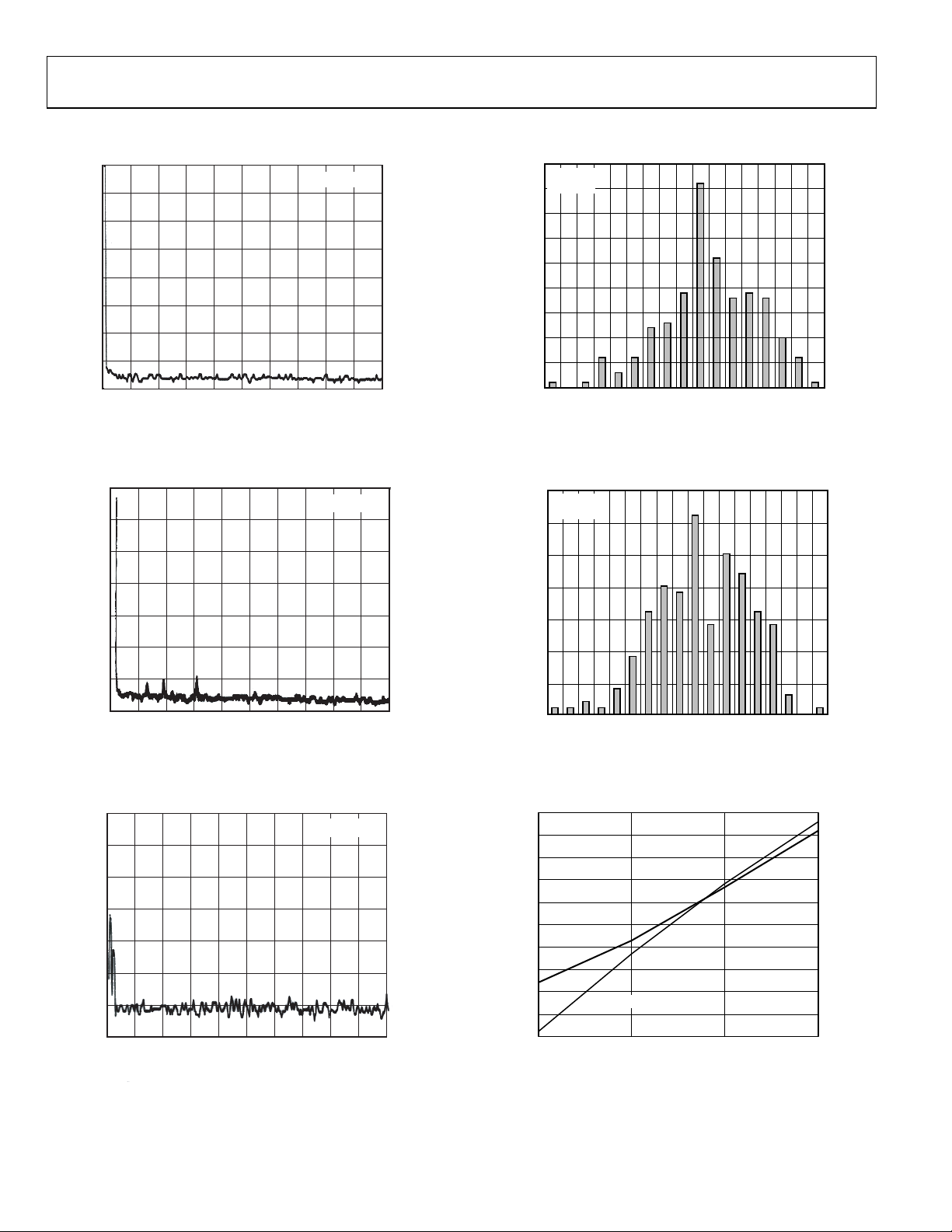
TYPICAL PERFORMANCE CHARACTERISTICS
32
28
24
20
16
12
8
VOLTAGE NOISE DENSITY (nV/√Hz)
4
0
0 102030405060708090100
FREQUENCY (Hz)
Figure 7. Voltage Noise Density vs. Frequency
VS = ±15V
03718-B-007
NUMBER OF AMPLIFIERS
45
VS = ±5V
T
= 25°C
A
40
35
30
25
20
15
10
5
0
–25 –5–15 0 45–30 –20 –10 5 10 15 20 25 30 35 40
–35
V
OS
Figure 10. Input Offset Voltage Distribution
(μV)
03718-B-010
31.5
27.0
22.5
18.0
13.5
9.0
VOLTAGE NOISE DENSITY (nV/√Hz)
4.5
0
0 0.1 0.2 0.3 0.4 0.5 0.6 0.7 0.8 0.9 1.0
FREQUENCY (kHz)
VS = ±15V
Figure 8. Voltage Noise Density vs. Frequency
VOLTAGE NOISE DENSITY (nV/√Hz)
17.5
15.0
12.5
10.0
7.5
5.0
2.5
0
110234567890
FREQUENCY (kHz)
VS = ±15V
Figure 9. Voltage Noise Density vs. Frequency
35
VS = ±15V
= 25°C
T
A
30
25
20
15
10
NUMBER OF AMPL IFIERS
5
0
–25 –5–15 0 50–30 –20 –10 5 10 15 20 25 30 35 40
–35
03718-B-008
(μV)
V
OS
45
03718-B-011
Figure 11. Input Offset Voltage Distribution
16
15
14
13
V)
μ
12
(
OS
V
11
10
V
= ±5V
S
9
8
7
6
–40 8525 125
03718-B-009
VS = ±15V
TEMPERATURE (°C)
03718-B-012
Figure 12. Input Offset Voltage vs. Temperature
Rev. E | Page 6 of 20

AD8671/AD8672/AD8674
5.0
4.5
4.0
3.5
3.0
2.5
(nA)
B
I
2.0
–I
B
1.5
1.0
0.5
0
–40 8525 125
+I
B
TEMPERATURE (°C)
Figure 13. Input Bias Current vs. Temperature
2.5
2.0
–I
1.5
B
VS=±5V
VS= ±15V
03718-B-013
14.5
14.0
13.5
13.0
12.5
12.0
11.5
OUTPUT VOLTAGE (V)
11.0
10.5
10.0
–40 8525 125
RL= 2k
Ω
RL= 600
Ω
TEMPERATURE (°C)
VS= ±15V
Figure 16. Output Voltage High vs. Temperature
–11.0
–11.5
–12.0
03718-B-016
VS= ±15V
1.0
(nA)
B
I
0.5
+I
B
0
–0.5
–1.0
–40 8525 125
TEMPERATURE (°C)
Figure 14. Input Bias Current vs. Temperature
4.0
3.8
3.6
3.4
(mA)
3.2
SY
I
3.0
VS = ±15V
2.8
2.6
VS=±5V
2.4
–40 8525 125
TEMPERATURE (°C)
–12.5
–13.0
OUTPUT VOLTAGE (V)
–13.5
–14.0
–14.5
–40 8525 125
03718-B-014
RL = 2k
RL= 600
Ω
Ω
TEMPERATURE (°C)
03718-B-017
Figure 17. Output Voltage Low vs. Temperature
60
50
GAIN
40
30
20
10
0
–10
OPEN-LOOP GAIN (dB)
–20
–30
–40
100k
03718-B-015
1M
FREQUENCY (Hz)
10M
VSY = ±15V
= 10kΩ
R
L
= 20pF
C
L
Φ
M
= 59°
PHASE
270
225
180
135
90
45
0
–45
–90
–135
–180
OPEN-LOOP PHASE (dB)
03718-B-018
Figure 15. Supply Current vs. Temperature
Figure 18. Open-Loop Gain and Phase Shift vs. Frequency
Rev. E | Page 7 of 20

AD8671/AD8672/AD8674
30000
±5V
25000
20000
15000
(V/mV)
VO
A
±15V
10000
5000
VSY = ±15V
V
= 4V
IN
R
= 2k
Ω
L
VOLTAGE (1V/DIV)
0
–40 8525 125
TEMPERATURE (°C)
Figure 19. Open-Loop Gain vs. Temperature
CLOSED-LOOP GAIN (dB)
50
40
30
20
10
0
–10
–20
–30
–40
–50
AV = 100
A
= 10
V
A
= 1
V
1k 1M
100k10k
FREQUENCY (Hz)
VSY = ±15V
V
IN
R
= ∞
L
C
= 20pF
L
10M
Figure 20. Closed-Loop Gain vs. Frequency
100
90
80
70
60
50
40
IMPEDANCE (Ω)
30
20
10
0
100
AVO = 100
1k 10M
FREQUENCY (Hz)
AVO = 10
AVO = 1
100k10k 100M
1M
Figure 21. Output Impedance vs. Frequency
= 10mV
100M
TIME (100μs/DIV)
03718-B-019
03718-B-022
Figure 22. Large Signal Transient Response
VSY = ±15V
V
= 200mV p-p
IN
R
= 2kΩ
L
VOLTAGE (50mV/DIV)
TIME (10μs/DIV)
03718-B-020
03718-B-023
Figure 23. Small Signal Transient Response
60
50
–OS
40
30
20
SMALL SIGNAL OVERSHOOT (%)
10
+OS
0
100
03718-B-021
1k
CAPACITANCE (pF)
VS =±15
10k
03718-B-024
Figure 24. Small Signal Overshoot vs. Load Capacitance
Rev. E | Page 8 of 20

AD8671/AD8672/AD8674
VOLTAGE (200mV/DIV)
VS = ±15V
= 200mV p-p
V
IN
= –100
A
V
= 10kΩ
R
L
V
IN
V
OUT
TIME (4μs/DIV)
Figure 25. Positive Overdrive Recovery
V
IN
VSY = ±15V
V
= 200mV p-p
IN
A
= –100
V
R
= 10kΩ
L
160
140
PSRR (dB)
120
100
–20
–40
80
60
40
20
0
10
100
1k 1M
FREQUENCY (Hz)
+PSRR
100k10k 10M
0V
0V
03718-B-025
Figure 28. PSRR v s. Frequency
135
134
133
0V
132
VS= ±2.5V TO ±18V
–PSRR
VSY = ±15V
03718-B-028
131
0V
VOLTAGE (200mV/DIV)
V
OUT
TIME (4μs/DIV)
03718-B-026
Figure 26. Negative Overdrive Recovery
CMRR (dB)
160
140
120
100
–20
–40
80
60
40
20
0
1k 1M
100
10
100k10k
FREQUENCY (Hz)
VSY = ±15V
10M
100M
03718-B-027
PSRR (dB)
130
129
128
127
–40 8525 125
TEMPERATURE (°C)
Figure 29. PSRR vs. Temperature
VS = ±15V
VOLTAGE NOISE (50nV/DIV)
TIME (1μs/DIV)
03718-B-029
03718-B-030
Figure 27. CMRR vs. Frequen cy
Figure 30. 0.1 Hz to 10 Hz Input Voltage Noise
Rev. E | Page 9 of 20

AD8671/AD8672/AD8674
0
–20
–40
–60
–80
–100
CHANNEL SEPARATION (dB)
–120
–140
100
1k 10k 100k 1M
FREQUENCY (Hz)
Figure 31. Channel Separation
VS = ±15V, ±5V
10M 100M
03718-B-031
Rev. E | Page 10 of 20

AD8671/AD8672/AD8674
APPLICATIONS
POWER DISSIPATION CALCULATIONS
To achieve low voltage noise in a bipolar op amp, the current
must be increased. The emitter-base theoretical voltage noise is
approximately
2
9
10
kTe =
n
qI
C
HznV/
Therefore, the rise above ambient temperature is
504 mW × 112°C/W = 56°C
With an ambient temperature of 50°C, the junction temperature
is 106°C. This is less than the specified absolute maximum junction
temperature, but for systems with long product lifetimes (years),
this should be considered carefully.
To achieve the low voltage noise of 2.8 nV/√Hz, the input stage
current is higher than most op amps with an equivalent gain
bandwidth product. The thermal noise of a 1 k resistor is
4 nV/√Hz, which is higher than the voltage noise of AD8671
family. Low voltage noise requires using low values of resistors,
so low voltage noise op amps should have good drive capability,
such as a 600 load. This means that the second stage and
output stage are also biased at higher currents. As a result, the
supply current of a single op amp is 3.5 mA maximum at room
temperature.
Junction temperature has a direct affect on reliability. For more
information, visit the following Analog Devices, Inc., website:
http://www.analog.com/en/quality-and-reliability/reliabilitydata/content/index.html
MTTF and FIT calculations can be done based on the junction
temperature and IC process. Use the following equation to
determine the junction temperature:
T
= TA + PD × θJA
J
For the AD8671 single in the 8-lead MSOP package, the thermal
resistance, θ
, is 142°C/W. If the ambient temperature is 30°C
JA
and the supply voltages are ±12 V, the power dissipation is
24 V × 3.5 mA = 84 mW
Therefore, the rise above ambient temperature is
84 mW × 142°C/W = 12°C
If the ambient temperature is 30°C, the junction temperature is
42°C. The previously mentioned website that details the effect
of the junction temperature on reliability has a calculator that
requires only the part number and the junction temperature to
determine the process technology.
Note that these calculations do not include the additional
dissipation caused by the load current on each op amp. Possible
solutions to reduce junction temperature include system level
considerations such as fans, Peltier thermoelectric coolers, and
heat pipes. Board considerations include operation on lower
voltages, such as ±12 V or ±5 V, and using two dual op amps
instead of one quad op amp. If the extremely low voltage noise
and high gain bandwidth is not required, using other quad op
amps, such as ADA4091-4, OP4177, ADA4004-4, OP497, or
AD704 can be considered.
UNITY-GAIN FOLLOWER APPLICATIONS
When large transient pulses (>1 V) are applied at the positive
terminal of amplifiers (such as the OP27, LT1007, OPA227, and
AD8671) with back-to-back diodes at the input stage, the use of
a resistor in the feedback loop is recommended to avoid having
the amplifier load the signal generator. The feedback resistor,
R
, should be at least 500 Ω. However, if large values must be
F
used for R
with R
capacitance and R
Figure 32 shows the uncompensated output response with a
10 kΩ resistor in the feedback and the compensated response
with C
, a small capacitor, CF, should be inserted in parallel
F
to compensate for the pole introduced by the input
F
.
F
= 15 pF.
F
OUTPUT UNCOMP E NSAT ED
OUTPUT
COMPENSATED
REF1 +OVER
23.23%
CH2 +OVER
7.885%
VOLTAGE (1V/ DI V)
For the AD8674 single in the 14-Lead TSSOP package, the thermal
resistance, θ
, is 112°C/W. Although θJA is lower than it is for the
JA
8-lead package, the four op amps are powered simultaneously. If
the ambient temperature is 50°C and the supply voltages are ±15 V,
the power dissipation is
30 V × 4.2 mA × four op amps = 504 mW
Rev. E | Page 11 of 20
TIME (100n s/ DIV)
Figure 32. Transient Output Response
03718-B-032

AD8671/AD8672/AD8674
OUTPUT PHASE REVERSAL
Phase reversal is a change of polarity in the amplifier transfer
function that occurs when the input voltage exceeds the supply
voltage. The AD8671/AD8672/AD8674 do not exhibit phase
reversal even when the input voltage is 1 V beyond the supplies.
VSY = ±15V
V
IN
V
VOLTAGE (1V/DIV)
OUT
TOTAL NOISE VS. SOURCE RESISTANCE
The low input voltage noise of the AD8671/AD8672/AD8674
makes them a great choice for applications with low source
resistance. However, because they have low input current noise,
they can also be used in circuits with substantial source
resistance.
Figure 34 shows the voltage noise, current noise, thermal noise,
and total rms noise of the AD8671 as a function of the source
resistance.
For R
< 475 Ω, the input voltage noise, en, dominates.
S
For 475 Ω < R
For R
> 412 kΩ, the input current noise dominates.
S
1000
< 412 kΩ, thermal noise dominates.
S
TIME (10μs/DIV)
Figure 33. Output Phase Reversal
100k
C
i
n
e
n
1M
03718-B-034
Hz)
100
03718-B-033
√
10
TOTAL NOISE (nV/
1
10
100 10k
e
n_t
(4kRST)
A
1k
SOURCE RESISTANCE (Ω)
1/2
B
Figure 34. Noise vs. Source Resistance
Rev. E | Page 12 of 20

AD8671/AD8672/AD8674
TOTAL HARMONIC DISTORTION (THD) AND NOISE
The AD8671/AD8672/AD8674 exhibit low total harmonic
distortion (THD) over the entire audio frequency range. This
makes them suitable for applications with high closed-loop
gains, including audio applications. Figure 35 shows
approximately 0.0006% of THD + N in a positive unity gain, the
worst-case configuration for distortion.
0.1000
0.0500
0.0200
0.0100
0.0050
0.0020
PERCENTAGE
0.0010
0.0005
0.0002
0.0001
100 1k 10k
5020 500200
LT1007
Hz
Figure 35. Total Harmonic Distortion and Noise
VS = ±5V
V
= 2.5V
IN
R
= 600Ω
L
AD8671
2k
5k
20k
03718-B-035
DRIVING CAPACITIVE LOADS
The AD8671/AD8672/AD8674 can drive large capacitive loads
without causing instability. However, when configured in unity
gain, driving very large loads can cause unwanted ringing or
instability.
Figure 36 shows the output of the AD8671 with a capacitive
load of 1 nF. If heavier loads are used in low closed-loop gain or
unity-gain configurations, it is recommended to use external
compensation as shown in the circuit in Figure 37. This
technique reduces the overshoot and prevents the op amp from
oscillation. The trade-off of this circuit is a reduction in output
swing. However, a great added benefit stems from the fact that
the input signal and the op amp’s noise are filtered, and thus the
overall output noise is kept to a minimum.
The output response of the circuit is shown in Figure 38.
VOLTAGE (500mV/DIV)
TIME (10μs/DIV)
Figure 36. AD8671 Capacitive Load Drive
V
R
500Ω
C
220pF
V
IN
F
G
CC
V
EE
Figure 37. Recommended Capacitive Load Circuit
VOLTAGE (100mV/DIV)
TIME (10μs/DIV)
Figure 38. Compensated Load Drive
R
500Ω
F
VSY = ±15V
R
= 2kΩ
L
C
= 1nF
L
V
IN
A
= +1
V
R
S
10Ω
VSY = ±15V
R
C
C
V
IN
A
= 100mV
C
1nF
= 2kΩ
L
= 1nF
L
= 220pF
F
= 100mV
= +2
V
L
CH2 +OVER
39.80%
CH2 –OVER
39.80%
R
L
2kΩ
CH2 +OVER
5.051%
CH2 –OVER
6.061%
03718-B-038
03718-B-037
03718-B-036
Rev. E | Page 13 of 20

AD8671/AD8672/AD8674
C
K
LOW NOISE OP AMP
BAND-PASS FILTER
AD8671
AD8671
GPS RECEIVER
GPS receivers require low noise to minimize RF effects. The
precision of the AD8671 makes it an excellent choice for such
applications. Its very low noise and wide bandwidth make it
suitable for band-pass and low-pass filters without the penalty
of high power consumption.
MIXER
AD831
Figure 39. Simplified Block Diagram of a GPS Receiver
DEMODULATOR
AD630
CODE GENERATOR
The band-pass response is shown in Figure 41.
LOW-PASS FILTER
AD8610
VS = ±15V
VGA
AD8369
ADC
AD10200
03718-B-039
Figure 39 shows a simplified block diagram of a GPS receiver.
The next section details the design equations.
BAND-PASS FILTER
Filters are useful in many applications; for example, band-pass
filters are used in GPS systems, as discussed in the previous
section. Figure 40 shows a second-order band-pass KRC filter.
R3
2.25kΩ
V
CC
R1
2.25kΩ
V
IN
The equal component topology yields a center frequency
2
foπ=
and
2
Q−=
R
2
4
where:
C2
1nF
1nF
C2
R2
2.25kΩ
V
EE
Figure 40. Band-Pass KRC Filter
18kΩ
R
B
R
10kΩ
A
03718-B-040
V/DIV
μ
200
100k1k100 10k 1M
Hz
10M
03718-B-041
Figure 41. Band-Pass Response
PLL SYNTHESIZERS AND LOOP FILTERS
Phase-lock loop filters are used in AM/FM modulation.
Loop filters in PLL design require accuracy and care in their
implementation. The AD8671/AD8672/AD8674 are ideal
candidates for such filter design; the low offset voltage and low
input bias current minimize the output error. In addition to the
excellent dc specifications, the AD8671/AD8672/AD8674 have
a unique performance at high frequencies; the high open-loop
gain and wide bandwidth allow the user to design a filter with a
high closed-loop gain if desirable. To optimize the filter design,
it is recommended to use small value resistors to minimize the
thermal noise. A simple example is shown in Figure 42.
C1
R1
10kΩ
1nF
V
CC
PHASE
DETECTOR
CHARGE
PUMP
VCO
K +=1
R
B
R
A
Figure 42. PLL Filter Simplified Block Diagram
D
V
EE
IN
03718-B-042
Rev. E | Page 14 of 20

AD8671/AD8672/AD8674
OUTLINE DIMENSIONS
5.00(0.1968)
4.80(0.1890)
4.00 (0.1574)
3.80 (0.1497)
0.25 (0.0098)
0.10 (0.0040)
COPLANARITY
0.10
CONTROLLING DIMENSIONS ARE IN MILLIMETERS; INCH DIMENSIONS
(IN PARENTHESES)ARE ROUNDED-OFF MILLIMETER EQUIVALENTS FOR
REFERENCE ONLYAND ARE NOT APPROPRIATE FOR USE IN DESIGN.
85
1
1.27 (0.0500)
SEATING
PLANE
COMPLIANT TO JEDEC STANDARDS MS-012-AA
BSC
6.20 (0.2441)
5.80 (0.2284)
4
1.75 (0.0688)
1.35 (0.0532)
0.51 (0.0201)
0.31 (0.0122)
8°
0°
0.25 (0.0098)
0.17 (0.0067)
0.50 (0.0196)
0.25 (0.0099)
1.27 (0.0500)
0.40 (0.0157)
45°
012407-A
Figure 43. 8-Lead Standard Small Outline Package [SOIC_N]
Narrow Body
(R-8)
Dimensions shown in millimeters and (inches)
3.20
3.00
2.80
8
5
3.20
3.00
2.80
PIN 1
IDENTIFIER
0.95
0.85
0.75
0.15
0.05
COPLANARITY
1
0.65 BSC
0.10
COMPLIANT TO JEDEC STANDARDS MO-187-AA
Figure 44. 8-Lead Mini Small Outline Package [MSOP]
5.15
4.90
4.65
4
15° MAX
6°
0°
0.23
0.09
0.40
0.25
1.10 MAX
(RM-8)
Dimensions shown in millimeters
0.80
0.55
0.40
100709-B
Rev. E | Page 15 of 20

AD8671/AD8672/AD8674
4.00 (0.1575)
3.80 (0.1496)
0.25 (0.0098)
0.10 (0.0039)
COPLANARITY
0.10
CONTROLLING DIMENSIONSARE IN MILLIMETERS; INCH DIMENSIONS
(IN PARENTHESES) ARE ROUNDED-OFF MILLI M E TER EQUIVALENTS FOR
REFERENCE ONLYAND ARE NOT AP PROPRIATE FOR USE IN DESIGN.
8.75 (0.3445)
8.55 (0.3366)
BSC
8
6.20 (0.2441)
5.80 (0.2283)
7
1.75 (0.0689)
1.35 (0.0531)
SEATING
PLANE
0.25 (0.0098)
0.17 (0.0067)
14
1
1.27 (0.0500)
0.51 (0.0201)
0.31 (0.0122)
COMPLIANT TO JEDEC STANDARDS MS-012-AB
0.50 (0.0197)
0.25 (0.0098)
8°
0°
1.27 (0.0500)
0.40 (0.0157)
45°
060606-A
Figure 45. 14-Lead Standard Small Outline Package [SOIC_N]
Narrow Body
(R-14)
Dimensions shown in millimeters and (inches)
5.10
5.00
4.90
4.50
4.40
4.30
PIN 1
1.05
1.00
0.80
0.15
0.05
COPLANARITY
0.10
14
1
0.65 BSC
0.30
0.19
COMPLIANT TO JEDEC S TANDARDS MO-153-AB-1
Figure 46. 14-Lead Thin Shrink Small Outline Package [TSSOP]
8
6.40
BSC
7
1.20
0.20
MAX
0.09
SEATING
PLANE
8°
0°
(RU-14)
Dimensions shown in millimeters
0.75
0.60
0.45
061908-A
Rev. E | Page 16 of 20

AD8671/AD8672/AD8674
ORDERING GUIDE
Model1 Temperature Range Package Description Package Option Branding
AD8671AR –40°C to +125°C 8-Lead SOIC_N R-8
AD8671AR-REEL –40°C to +125°C 8-Lead SOIC_N R-8
AD8671AR-REEL7 –40°C to +125°C 8-Lead SOIC_N R-8
AD8671ARZ –40°C to +125°C 8-Lead SOIC_N R-8
AD8671ARZ-REEL –40°C to +125°C 8-Lead SOIC_N R-8
AD8671ARZ-REEL7 –40°C to +125°C 8-Lead SOIC_N R-8
AD8671ARMZ –40°C to +125°C 8-Lead MSOP RM-8 A0V
AD8671ARMZ-REEL –40°C to +125°C 8-Lead MSOP RM-8 A0V
AD8672AR –40°C to +125°C 8-Lead SOIC_N R-8
AD8672AR-REEL –40°C to +125°C 8-Lead SOIC_N R-8
AD8672AR-REEL7 –40°C to +125°C 8-Lead SOIC_N R-8
AD8672ARZ –40°C to +125°C 8-Lead SOIC_N R-8
AD8672ARZ-REEL –40°C to +125°C 8-Lead SOIC_N R-8
AD8672ARZ-REEL7 –40°C to +125°C 8-Lead SOIC_N R-8
AD8672ARMZ –40°C to +125°C 8-Lead MSOP RM-8 A0W
AD8672ARMZ-REEL –40°C to +125°C 8-Lead MSOP RM-8 A0W
AD8674AR –40°C to +85°C 14-Lead SOIC_N R-14
AD8674ARZ –40°C to +85°C 14-Lead SOIC_N R-14
AD8674ARZ-REEL –40°C to +85°C 14-Lead SOIC_N R-14
AD8674ARZ-REEL7 –40°C to +85°C 14-Lead SOIC_N R-14
AD8674ARU –40°C to +85°C 14-Lead TSSOP RU-14
AD8674ARUZ –40°C to +85°C 14-Lead TSSOP RU-14
AD8674ARUZ-REEL –40°C to +85°C 14-Lead TSSOP RU-14
1
Z = RoHS Compliant Part.
Rev. E | Page 17 of 20

AD8671/AD8672/AD8674
NOTES
Rev. E | Page 18 of 20

AD8671/AD8672/AD8674
NOTES
Rev. E | Page 19 of 20

AD8671/AD8672/AD8674
NOTES
©2004–2010 Analog Devices, Inc. All rights reserved. Trademarks and
registered trademarks are the property of their respective owners.
D03718–0–6/10(E)
Rev. E | Page 20 of 20
 Loading...