

Precision, Very Low Noise, Low Input
–
+
–
+
FEATURES
Very low noise: 2.8 nV/√Hz, 77 nV p-p
Wide bandwidth: 10 MHz
Low input bias current: 12 nA max
Low offset voltage: 75 µV max
High open-loop gain: 120 dB min
Low supply current: 3 mA per amplifier
Dual-supply operation: ±5 V to ±15 V
Unity gain stable
No phase reversal
APPLICATIONS
PLL filters
Filters for GPS
Instrumentation
Sensors and controls
Professional quality audio
GENERAL DESCRIPTION
The AD8671/AD8672/AD8674 are very high precision
amplifiers featuring very low noise, very low offset voltage and
drift, low input bias current, 10 MHz bandwidth, and low power
consumption. Outputs are stable with capacitive loads of over
1000 pF. Supply current is less than 3 mA per amplifier at 30 V.
The AD8671’s combination of ultralow noise, high precision,
speed, and stability is unmatched, while the MSOP version
requires only half the board space of comparable amplifiers.
Applications for these amplifiers include high quality PLL
filters, precision filters, medical and analytical instrumentation,
precision power supply controls, ATE, data acquisition, and
precision controls as well as professional quality audio.
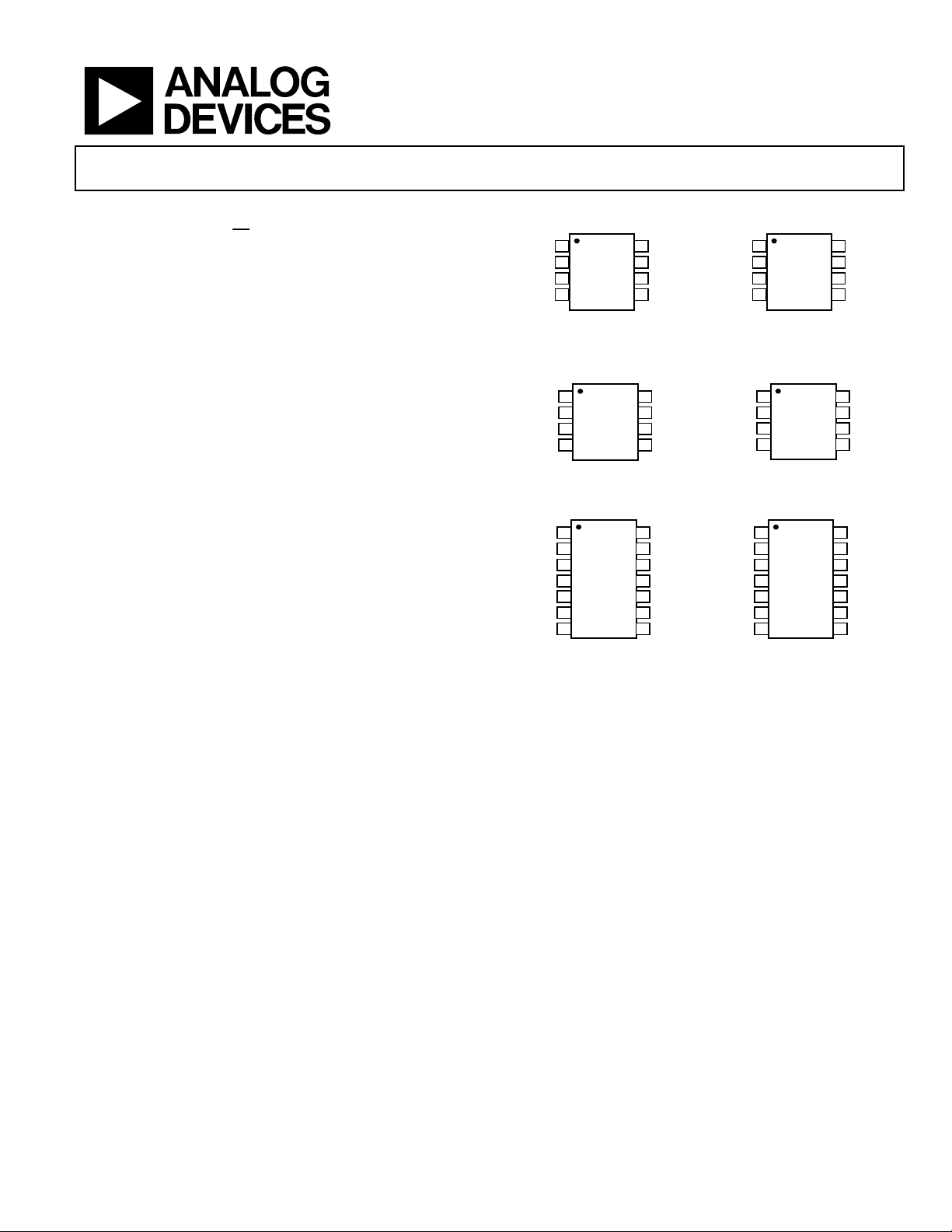
Bias Current
NC
1
AD8671
2
IN
TOP VIEW
IN
3
(Not to Scale)
V–
4
NC = NO CONNECT
Figure 1. 8-Lead SOIC (R Suffix)
1
OUT A
–IN A
+IN A
Figure 3. 8-Lead SOIC (R Suffix)
OUT A
–IN A
+IN A
+IN B
–IN B
OUT B
Figure 5. 14-Lead SOIC (R Suffix) Figure 6. 14-Lead TSSOP (RU Suffix)
V–
V+
AD8672
2
TOP VIEW
3
(Not to Scale)
4
1
2
3
AD8674
4
TOP VIEW
(Not to Scale)
5
6
7
Operational Amplifiers
AD8671/AD8672/AD8674
PIN CONFIGURATIONS
NC
8
7
6
5
14
13
12
11
10
9
8
8
7
6
5
V+
OUT
NC
V+
OUT B
–IN B
+IN B
OUT D
–IN D
+IN D
V–
+IN C
–IN C
OUT C
03718-B-001
NC
1
AD8671
2
IN
TOP VIEW
IN
3
(Not to Scale)
V–
4
NC = NO CONNECT
Figure 2. 8-Lead MSOP (RM Suffix)
OUT A
1
V–
AD8672
2
TOP VIEW
3
(Not to Scale)
4
–IN A
+IN A
03718-B-003
Figure 4. 8-Lead MSOP (RM Suffix)
OUT A
1
2
–IN A
+IN A
3
AD8674
V+
4
TOP VIEW
(Not to Scale)
–IN B
5
6
+IN B
OUT B
03718-B-005
7
8
7
6
5
14
13
12
11
10
9
8
8
7
6
5
NC
V+
OUT
NC
03718-B-002
V+
OUT B
–IN B
+IN B
OUT D
–IN D
+IN D
V–
+IN C
–IN C
OUT C
03718-B-004
03718-B-006
The AD8671/AD8672/AD8674 are specified over the extended
industrial (–40°C to +125°C) temperature range.
The AD8671/AD8672 are available in the 8-lead SOIC and
8-lead MSOP packages. The AD8674 is available in 14-lead
SOIC and 14-lead TSSOP packages.
Surface-mount devices in MSOP packages are available in tape
and reel only.
Rev. B
Information furnished by Analog Devices is believed to be accurate and reliable.
However, no responsibility is assumed by Analog Devices for its use, nor for any
infringements of patents or other rights of third parties that may result from its use.
Specifications subject to change without notice. No license is granted by implication
or otherwise under any patent or patent rights of Analog Devices. Trademarks and
registered trademarks are the property of their respective owners.
One Technology Way, P.O. Box 9106, Norwood, MA 02062-9106, U.S.A.
Tel: 781.329.4700
Fax: 781.326.8703 © 2004 Analog Devices, Inc. All rights reserved.
www.analog.com

AD8671/AD8672/AD8674
TABLE OF CONTENTS
Specifications..................................................................................... 3
Tot a l N o is e v s . So u rc e Re si s ta nc e ............................................. 11
Electrical Characteristics, ±5.0 V................................................ 3
Electrical Characteristics, ±15 V................................................. 4
Absolute Maximum Ratings............................................................ 5
Typical Performance Characteristics............................................. 6
Applications..................................................................................... 11
Unity Gain Follower Applications............................................ 11
Output Phase Reversal............................................................... 11
REVISION HISTORY
4/04—Data Sheet Changed from Rev. A to Rev. B
Changes to Figure 32.................................................................. 11
Changes to Figures 36, 37, and 38............................................. 12
1/04—Data Sheet Changed from Rev. 0 to Rev. A
Added AD8672 and AD8674 parts ..............................Universal
Changes to Specifications............................................................ 3
Deleted Figure 3............................................................................ 6
Changes to Figures 7, 8, and 9..................................................... 6
Changes to Figure 37.................................................................. 12
Added new Figure 32 ................................................................. 10
THD + Noise............................................................................... 12
Driving Capacitive Loads.......................................................... 12
GPS Receiver............................................................................... 13
Band-Pass Filter.......................................................................... 13
PLL Synthesizers and Loop Filters........................................... 13
Outline Dimensions....................................................................... 14
Ordering Guide............................................................................... 16
Rev. B | Page 2 of 16

AD8671/AD8672/AD8674
SPECIFICATIONS
ELECTRICAL CHARACTERISTICS, ±5.0 V
Table 1. VS = ±5.0 V, VCM = 0 V, TA = 25°C, unless otherwise noted
Parameter Symbol Conditions Min Typ Max Unit
INPUT CHARACTERISTICS
Offset Voltage V
OS
–40°C < TA < +125°C 30 125 µV
Offset Voltage Drift ∆VOS/∆T –40°C < TA < +125°C
AD8671 0.3 0.5 µV/°C
AD8672/AD8674 0.3 0.8 µV/°C
Input Bias Current I
B
+25°C < TA < +125°C –20 +5 +20 nA
–40°C < TA < +125°C –40 +8 +40 nA
Input Offset Current I
OS
+25°C < TA < +125°C –20 +6 +20 nA
–40°C < TA < +125°C –40 +8 +40 nA
Input Voltage Range –2.5 +2.5 V
Common-Mode Rejection Ratio CMRR VCM = –2.5 V to +2.5 V 100 120 dB
Large Signal Voltage Gain A
Input Capacitance, Common Mode C
Input Capacitance, Differential Mode C
Input Resistance, Common Mode R
Input Resistance, Differential Mode R
VO
INCM
INDM
IN
INDM
OUTPUT CHARACTERISTICS
Output Voltage High V
Output Voltage Low V
Output Voltage High V
Output Voltage Low V
Output Current I
OH
OL
OH
OL
OUT
POWER SUPPLY
Power Supply Rejection Ratio PSRR VS = ±4 V to ±18 V
AD8671/AD8672 110 130 dB
AD8674 106 115 dB
Supply Current/Amplifier I
SY
–40°C <TA < +125°C 4.2 mA
DYNAMIC PERFORMANCE
Slew Rate SR RL = 2 kΩ 4 V/µs
Settling Time t
S
To 0.01% (4 V Step, G = 1) 5.1 µs
Gain Bandwidth Product GBP 10 MHz
NOISE PERFORMANCE
Peak-to-Peak Noise e
Voltage Noise Density e
Current Noise Density i
n p-p
n
n
Channel Separation
AD8672/AD8674 Cs f = 1 kHz –130 dB
f = 10 kHz –105 dB
20 75 µV
–12 +3 +12 nA
–12 +6 +12 nA
RL = 2 kΩ, VO = –3 V to +3 V 1000 6000 V/mV
6.25 pF
7.5 pF
3.5 GΩ
15 MΩ
RL = 2 kΩ, –40°C to +125°C +3.8 +4.0 V
RL = 2 kΩ, –40°C to +125°C –3.9 –3.8 V
RL = 600 Ω +3.7 +3.9 V
RL = 600 Ω –3.8 –3.7 V
±10 mA
VO = 0 V 3 3.5 mA
To 0.1% (4 V Step, G = 1) 1.4 µs
0.1 Hz to 10 Hz 77 100 nV p-p
f = 1 kHz 2.8 3.8
f = 1 kHz 0.3
nV/√
pA/√
Hz
Hz
Rev. B | Page 3 of 16

AD8671/AD8672/AD8674
ELECTRICAL CHARACTERISTICS, ±15 V
Table 2. VS = ±15 V, VCM = 0 V, TA = 25°C, unless otherwise noted
Parameter Symbol Conditions Min Typ Max Unit
INPUT CHARACTERISTICS
Offset Voltage V
OS
–40°C < TA < +125°C 30 125 µV
Offset Voltage Drift ∆VOS/∆T –40°C < TA < +125°C
AD8671 0.3 0.5 µV/°C
AD8672/AD8674 0.3 0.8 µV/°C
Input Bias Current I
B
+25°C < TA < +125°C –20 +5 +20 nA
–40°C < TA < +125°C –40 +8 +40 nA
Input Offset Current I
OS
+25°C < TA < +125°C –20 +6 +20 nA
–40°C < TA < +125°C –40 +8 +40 nA
Input Voltage Range –12 +12 V
Common-Mode Rejection Ratio CMRR VCM = –12 V to +12 V 100 120 dB
Large Signal Voltage Gain A
Input Capacitance, Common Mode C
Input Capacitance, Differential Mode C
Input Resistance, Common Mode R
Input Resistance, Differential Mode R
VO
INCM
INDM
IN
INDM
OUTPUT CHARACTERISTICS
Output Voltage High V
Output Voltage Low V
Output Voltage High V
Output Voltage Low V
Output Current I
Short Circuit Current I
OH
OL
OH
OL
OUT
SC
POWER SUPPLY
Power Supply Rejection Ratio PSRR VS = ±4 V to ±18 V
AD8671/AD8672 110 130 dB
AD8674 106 115 dB
Supply Current/Amplifier I
SY
–40°C <TA < +125°C 4.2 mA
DYNAMIC PERFORMANCE
Slew Rate SR RL = 2 kΩ 4 V/µs
Settling Time t
S
To 0.01% (10 V Step, G = 1) 6.3 µs
Gain Bandwidth Product GBP 10 MHz
NOISE PERFORMANCE
Peak-to-Peak Noise e
Voltage Noise Density e
Current Noise Density i
n p-p
n
n
Channel Separation
AD8672/AD8674 Cs f = 1 kHz –130 dB
f = 10 kHz –105 dB
20 75 µV
–12 +3 +12 nA
–12 +6 +12 nA
RL = 2 kΩ, VO = –10 V to +10 V 1000 6000 V/mV
6.25 pF
7.5 pF
3.5 GΩ
15 MΩ
RL = 2 kΩ, –40°C to +125°C +13.2 +13.8 V
RL = 2 kΩ, –40°C to +125°C –13.8 –13.2 V
RL = 600 Ω +11 +12.3 V
RL = 600 Ω –12.4 –11 V
±20 mA
±30 mA
VO = 0 V 3 3.5 mA
To 0.1% (10 V Step, G = 1) 2.2 µs
0.1 Hz to 10 Hz 77 100 nV p-p
f = 1 kHz 2.8 3.8
f = 1 kHz 0.3
nV/√
pA/√
Hz
Hz
Rev. B | Page 4 of 16
AD8671/AD8672/AD8674
ABSOLUTE MAXIMUM RATINGS
Table 3. AD8671/AD8672/AD8674 Stress Ratings
Parameter Rating
Supply Voltage 36 V
Input Voltage VS– to VS+
Differential Input Voltage ±0.7 V
Output Short-Circuit Duration Indefinite
Storage Temperature Range
All Packages –65°C to +150°C
Operating Temperature Range
All Packages –40°C to +125°C
Junction Temperature Range
All Packages –65°C to +150°C
Lead Temperature Range (Soldering, 60 sec) 300°C
Stresses above those listed under Absolute Maximum Ratings
may cause permanent damage to the device. This is a stress
rating only; functional operation of the device at these or any
other conditions above those indicated in the operational
section of this specification is not implied. Exposure to absolute
maximum rating conditions for extended periods may affect
device reliability.
1
Absolute maximum ratings apply at 25°C, unless otherwise noted.
ESD CAUTION
ESD (electrostatic discharge) sensitive device. Electrostatic charges as high as 4000 V readily accumulate on
the human body and test equipment and can discharge without detection. Although this product features
proprietary ESD protection circuitry, permanent damage may occur on devices subjected to high energy
electrostatic discharges. Therefore, proper ESD precautions are recommended to avoid performance
degradation or loss of functionality.
1
Table 4. Package Characteristics
Package Type θ
2
JA
8-Lead MSOP (RM) 190 44 °C/W
8-Lead SOIC (R) 158 43 °C/W
14-Lead SOIC (R) 120 36 °C/W
14-Lead TSSOP (RU) 180 35 °C/W
2
θJA is specified for the worst-case conditions, i.e., θJA is specified for device
soldered in circuit board for surface-mount packages.
θ
JC
Unit
Rev. B | Page 5 of 16

AD8671/AD8672/AD8674
TYPICAL PERFORMANCE CHARACTERISTICS
32
28
24
20
16
12
8
VOLTAGE NOISE DENSITY (nV/ Hz)
4
0
0 102030405060708090100
FREQUENCY (Hz)
Figure 7. Voltage Noise Density vs. Frequency
31.5
27.0
VS = ±15V
VS = ±15V
03718-B-007
45
VS = ±5V
= 25°C
T
A
40
35
30
25
20
15
NUMBER OF AMPLIFIERS
10
5
0
–35
–25 –5–15 0 45–30 –20 –10 5 10 15 20 25 30 35 40
V
(µV)
OS
03718-B-010
Figure 10. Input Offset Voltage Distribution
35
VS = ±15V
= 25°C
T
A
30
22.5
18.0
13.5
9.0
VOLTAGE NOISE DENSITY (nV/ Hz)
4.5
0
0 0.1 0.2 0.3 0.4 0.5 0.6 0.7 0.8 0.9 1.0
FREQUENCY (kHz)
Figure 8. Voltage Noise Density vs. Frequency
17.5
15.0
12.5
10.0
7.5
5.0
2.5
VOLTAGE NOISE DENSITY (nV/ Hz)
0
110234567890
FREQUENCY (kHz)
VS = ±15V
Figure 9. Voltage Noise Density vs. Frequency
25
20
15
10
NUMBER OF AMPLIFIERS
5
0
–35
–25 –5–15 0 50–30 –20 –10 5 10 15 20 25 30 35 40
03718-B-008
V
(µV)
OS
45
03718-B-011
Figure 11. Input Offset Voltage Distribution
16
15
14
13
12
(µV)
OS
V
11
10
V
= ±5V
S
9
8
7
6
–40 8525 125
03718-B-009
VS = ±15V
TEMPERATURE (°C)
Figure 12. Input Offset Voltage vs. Temperature
03718-B-012
Rev. B | Page 6 of 16

AD8671/AD8672/AD8674
5.0
4.5
4.0
3.5
3.0
2.5
(nA)
B
I
2.0
–I
B
1.5
1.0
0.5
0
–40 8525 125
+I
B
TEMPERATURE (°C)
Figure 13. Input Bias Current vs. Temperature
2.5
2.0
–I
1.5
B
VS=±5V
VS= ±15V
03718-B-013
14.5
14.0
13.5
13.0
12.5
12.0
11.5
OUTPUT VOLTAGE (V)
11.0
10.5
10.0
–40 8525 125
RL= 2k
Ω
RL= 600
Ω
TEMPERATURE (°C)
VS= ±15V
Figure 16. Output Voltage High vs. Temperature
–11.0
–11.5
–12.0
03718-B-016
VS= ±15V
1.0
(nA)
B
I
0.5
+I
B
0
–0.5
–1.0
–40 8525 125
TEMPERATURE (°C)
Figure 14. Input Bias Current vs. Temperature
4.0
3.8
3.6
3.4
(mA)
3.2
SY
I
3.0
VS = ±15V
2.8
2.6
VS=±5V
2.4
–40 8525 125
TEMPERATURE (°C)
–12.5
–13.0
OUTPUT VOLTAGE (V)
–13.5
–14.0
–14.5
–40 8525 125
03718-B-014
RL = 2k
RL= 600
Ω
Ω
TEMPERATURE (°C)
03718-B-017
Figure 17. Output Voltage Low vs. Temperature
60
50
GAIN
40
30
20
10
0
–10
OPEN-LOOP GAIN (dB)
–20
–30
–40
100k
03718-B-015
1M
FREQUENCY (Hz)
10M
VSY = ±15V
= 10kΩ
R
L
= 20pF
C
L
Φ
M
= 59°
PHASE
270
225
180
135
90
45
0
–45
–90
–135
–180
OPEN-LOOP PHASE (dB)
03718-B-018
Figure 15. Supply Current vs. Temperature
Figure 18. Open-Loop Gain and Phase Shift vs. Frequency
Rev. B | Page 7 of 16

AD8671/AD8672/AD8674
30000
±5V
25000
20000
15000
(V/mV)
VO
A
±15V
10000
5000
VSY = ±15V
V
= 4V
IN
R
= 2kΩ
L
VOLTAGE (1V/DIV)
0
–40 8525 125
TEMPERATURE (°C)
Figure 19. Open-Loop Gain vs. Temperature
CLOSED-LOOP GAIN (dB)
50
40
30
20
10
0
–10
–20
–30
–40
–50
AV = 100
A
= 10
V
A
= 1
V
1k 1M
100k10k
FREQUENCY (Hz)
VSY = ±15V
V
IN
R
L
C
L
10M
= ∞
= 20pF
Figure 20. Closed-Loop Gain vs. Frequency
100
90
80
70
60
50
40
IMPEDANCE ( Ω )
30
20
10
0
100
AVO = 100
1k 10M
FREQUENCY (Hz)
AVO = 10
AVO = 1
100k10k 100M
1M
Figure 21. Output Impedance vs. Frequency
= 10mV
100M
TIME (100µs/DIV)
03718-B-019
03718-B-022
Figure 22. Large Signal Transient Response
VSY = ±15V
VIN = 200mV p-p
RL = 2kΩ
VOLTAGE (50mV/DIV)
TIME (10µs/DIV)
03718-B-020
03718-B-023
Figure 23. Small Signal Transient Response
60
50
–OS
40
30
20
SMALL SIGNAL OVERSHOOT (%)
10
+OS
0
100
03718-B-021
1k
CAPACITANCE (pF)
VS =±15
10k
03718-B-024
Figure 24. Small Signal Overshoot vs. Load Capacitance
Rev. B | Page 8 of 16

AD8671/AD8672/AD8674
VOLTAGE (200mV/DIV)
VS = ±15V
= 200mV p-p
V
IN
= –100
A
V
= 10kΩ
R
L
V
IN
V
OUT
TIME (4µs/DIV)
Figure 25. Positive Overdrive Recovery
V
IN
VSY = ±15V
= 200mV p-p
V
IN
A
= –100
V
RL = 10kΩ
160
140
PSRR (dB)
120
100
–20
–40
80
60
40
20
0
100
10
1k 1M
FREQUENCY (Hz)
+PSRR
100k10k 10M
0V
0V
03718-B-025
Figure 28. PSRR v s. Frequency
135
134
133
VS= ±2.5V TO ±18V
–PSRR
VSY = ±15V
03718-B-028
0V
0V
VOLTAGE (200mV/DIV)
V
OUT
TIME (4µs/DIV)
03718-B-026
Figure 26. Negative Overdrive Recovery
CMRR (dB)
160
140
120
100
–20
–40
80
60
40
20
0
1k 1M
100
10
100k10k
FREQUENCY (Hz)
VSY = ±15V
10M
100M
03718-B-027
132
131
PSRR (dB)
130
129
128
127
–40 8525 125
TEMPERATURE (°C)
Figure 29. PSRR vs. Temperature
VS = ±15V
VOLTAGE NOISE (50nV/DIV)
TIME (1µs/DIV)
03718-B-029
03718-B-030
Figure 27. CMRR vs. Fre quency
Figure 30. 0.1 Hz to 10 Hz Input Voltage Noise
Rev. B | Page 9 of 16

AD8671/AD8672/AD8674
0
–20
–40
–60
–80
–100
CHANNEL SEPARATION (dB)
–120
–140
100
1k 10k 100k
FREQUENCY (Hz)
Figure 31. Channel Separation
VS = ±15V, ±5V
1M
10M 100M
03718-B-031
Rev. B | Page 10 of 16

AD8671/AD8672/AD8674
APPLICATIONS
UNITY GAIN FOLLOWER APPLICATIONS
When large transient pulses (>1 V) are applied at the positive
terminal of amplifiers (such as the OP27, LT1007, OPA227, and
AD8671) with back-to-back diodes at the input stage, the use of
a resistor in the feedback loop is recommended to avoid having
the amplifier load the signal generator. The feedback resistor, R
should be at least 500 Ω. However, if large values must be used
, a small capacitor, CF, should be inserted in parallel with
for R
F
to compensate for the pole introduced by the input
R
F
capacitance and R
Figure 32 shows the uncompensated output response with a
10 kΩ resistor in the feedback and the compensated response
= 15 pF.
with C
F
.
F
V
IN
,
F
VOLTAGE (1V/DIV)
TIME (10µs/DIV)
Figure 33. Output Phase Reversal
V
OUT
VSY = ±15V
03718-B-033
OUTPUT UNCO M P ENSATED
OUTPUT
COMPENSATED
REF1 +OVER
23.23%
CH2 +OVER
7.885%
VOLTAGE (1V/DIV)
TIME (100ns/DIV)
03718-B-032
Figure 32. Transient Output Response
OUTPUT PHASE REVERSAL
Phase reversal is a change of polarity in the amplifier transfer
function that occurs when the input voltage exceeds the supply
voltage. The AD8671/AD8672/AD8674 do not exhibit phase
reversal even when the input voltage is 1 V beyond the supplies.
TOTAL NOISE VS. SOURCE RESISTANCE
The low input voltage noise of the AD8671 makes it a great
choice for applications with low source resistance. However,
because the AD8671 has low input current noise, it can also be
used in circuits with substantial source resistance.
Figure 34 shows the voltage noise, current noise, thermal noise,
and total rms noise of the AD8671 as a function of the source
resistance.
< 475 Ω, the input voltage noise, en, dominates.
For R
S
For 475 Ω < R
> 412 kΩ, the input current noise dominates.
For R
S
1000
100
10
TOTAL NOISE (nV/ Hz)
< 412 kΩ, thermal noise dominates.
S
e
n_t
1
10
100 10k
(4kRST)
A
1k
SOURCE RESISTANCE (Ω)
Figure 34. Noise vs. Source Resistance
C
i
n
1/2
B
100k
e
n
1M
03718-B-034
Rev. B | Page 11 of 16

AD8671/AD8672/AD8674
THD + NOISE
The AD8671/AD8672/AD8674 exhibit low total harmonic
distortion over the entire audio frequency range. This makes
them suitable for applications with high closed-loop gains,
including audio applications. Figure 35 shows approximately
0.0006% of THD + N in a positive unity gain, the worst-case
configuration for distortion.
0.1000
0.0500
0.0200
0.0100
0.0050
0.0020
PERCENTAGE
0.0010
0.0005
0.0002
0.0001
100 1k 10k
5020 500200
LT1007
Hz
Figure 35. Total Harmonic Noise and Distortion
DRIVING CAPACITIVE LOADS
The AD8671/AD8672/AD8674 can drive large capacitive loads
without causing instability. However, when configured in unity
gain, driving very large loads can cause unwanted ringing or
instability.
Figure 36 shows the output of the AD8671 with a capacitive
load of 1 nF. If heavier loads are to be used in low closed-loop
gain or unity gain configurations, it is recommended to use
external compensation as shown in the circuit in Figure 37. This
technique reduces the overshoot and prevents the op amp from
oscillation. The trade-off of this circuit is a reduction in output
swing. However, a great added benefit stems from the fact that
the input signal and the op amp’s noise are filtered, and thus the
overall output noise is kept to a minimum.
The output response of the circuit is shown in Figure 38.
VS = ±5V
= 2.5V
V
IN
R
= 600Ω
L
AD8671
2k
5k
20k
03718-B-035
VSY = ±15V
R
= 2kΩ
L
C
= 1nF
L
V
= 100mV
IN
A
= +1
V
VOLTAGE (500mV/DIV)
TIME (10µs/DIV)
CH2 +OVER
39.80%
CH2 –OVER
39.80%
03718-B-036
Figure 36. Capacitive Load Drive
R
F
500Ω
V
R
500Ω
C
G
F
220pF
V
IN
CC
R
S
10Ω
V
EE
C
1nF
L
R
L
2kΩ
03718-B-037
Figure 37. Recommended Capacitive Load Circuit
VSY = ±15V
= 2kΩ
R
L
= 1nF
C
L
= 220pF
C
F
= 100mV
V
IN
AV = +2
VOLTAGE (100mV/DI V )
TIME (10µs/DIV)
CH2 +OVER
5.051%
CH2 –OVER
6.061%
03718-B-038
Figure 38. Compensated Load Drive
Rev. B | Page 12 of 16

AD8671/AD8672/AD8674
R1
10kΩ
CC
ADC
AD10200
C1
1nF
03718-B-039
VCO
10M
03718-B-041
BAND-PASS FILTER
AD8671
LOW NOISE OP AMP
AD8671
MIXER
AD831
CODE GENERATOR
Figure 39. Simplified Block Diagram of a GPS Receiver
GPS RECEIVER
GPS receivers require low noise to minimize RF effects. The
precision of the AD8671 makes it an excellent choice for such
applications. Its very low noise and wide bandwidth make it
suitable for band-pass and low-pass filters without the penalty
of high power consumption.
Figure 39 shows a simplified block diagram of a GPS receiver.
The next section details the design equations.
BAND-PASS FILTER
Filters are useful in many applications; for example, band-pass
filters are used in GPS systems, as discussed in the previous
section. Figure 40 shows a second-order band-pass KRC filter.
R3
2.25kΩ
V
CC
R1
2.25kΩ
V
IN
The equal component topology yields a center frequency
2
RCfoπ=2
and
2
KQ−=4
where:
C2
1nF
1nF
C2
2.25kΩ
R2
V
EE
Figure 40. Band-Pass KRC Filter
18kΩ
R
B
R
10kΩ
A
03718-B-040
DEMODULATOR
AD630
The band-pass response is shown in Figure 41.
PLL SYNTHESIZERS AND LOOP FILTERS
Phase-lock loop filters are used in AM/FM modulation.
Loop filters in PLL design require accuracy and care in their
implementation. The AD8671/AD8672/AD8674 are ideal
candidates for such filter design; the low offset voltage and low
input bias current minimize the output error. In addition to the
excellent dc specifications, the AD8671/AD8672/AD8674 have
a unique performance at high frequencies; the high open-loop
gain and wide bandwidth allow the user to design a filter with a
high closed-loop gain if desirable. To optimize the filter design,
it is recommended to use small value resistors to minimize the
thermal noise. A simple example is shown in Figure 42.
LOW-PASS FILTER
AD8610
VS = ±15V
200µV/DIV
PHASE
DETECTOR
VGA
AD8369
100k1k100 10k 1M
Hz
Figure 41. Band-Pass Response
V
CHARGE
PUMP
R
K += 1
B
R
A
Figure 42. PLL Filter Simplified Block Diagram
D
V
EE
IN
03718-B-042
Rev. B | Page 13 of 16

AD8671/AD8672/AD8674
Y
OUTLINE DIMENSIONS
4.00 (0.1574)
3.80 (0.1497)
5.00 (0.1968)
4.80 (0.1890)
85
6.20 (0.2440)
5.80 (0.2284)
41
1.27 (0.0500)
BSC
0.25 (0.0098)
0.10 (0.0040)
COPLANARIT
0.10
CONTROLLING DIMENSIONS ARE IN MILLIMETERS; INCH DIMENSIONS
(IN PARENTHESES) ARE ROUNDED-OFF MILLIMETER EQUIVALENTS FOR
REFERENCE ONLY AND ARE NOT APPROPRIATE FOR USE IN DESIGN
SEATING
PLANE
COMPLIANT TO JEDEC STANDARDS MS-012AA
1.75 (0.0688)
1.35 (0.0532)
0.51 (0.0201)
0.31 (0.0122)
0.25 (0.0098)
0.17 (0.0067)
0.50 (0.0196)
0.25 (0.0099)
8°
1.27 (0.0500)
0°
0.40 (0.0157)
× 45°
Figure 43. 8-Lead Standard Small Outline Package [SOIC]
(R-8)
Dimensions shown in millimeters and (inches)
3.00
BSC
85
3.00
BSC
PIN 1
0.65 BSC
0.15
0.00
0.38
0.22
COPLANARITY
0.10
COMPLIANT TO JEDEC STANDARDS MO-187AA
Figure 44. 8-Lead Micro Small Outline Package [MSOP]
4.90
BSC
4
1.10 MAX
8°
0°
SEATING
PLANE
0.23
0.08
(RM-8)
Dimensions shown in millimeters
0.80
0.60
0.40
Rev. B | Page 14 of 16

AD8671/AD8672/AD8674
8.75 (0.3445)
8.55 (0.3366)
4.00 (0.1575)
3.80 (0.1496)
0.25 (0.0098)
0.10 (0.0039)
COPLANARITY
0.10
CONTROLLING DIMENSIONS ARE IN MILLIMETERS; INCH DIMENSIONS
(IN PARENTHESES) ARE ROUNDED-OFF MILLIMETER EQUIVALENTS FOR
REFERENCE ONLY AND ARE NOT APPROPRIATE FOR USE IN DESIGN
14
1
1.27 (0.0500)
BSC
0.51 (0.0201)
0.31 (0.0122)
COMPLIANT TO JEDEC STANDARDS MS-012AB
8
6.20 (0.2441)
7
5.80 (0.2283)
SEATING
PLANE
1.75 (0.0689)
1.35 (0.0531)
0.25 (0.0098)
0.17 (0.0067)
0.50 (0.0197)
0.25 (0.0098)
8°
0°
1.27 (0.0500)
0.40 (0.0157)
× 45°
Figure 45. 14-Lead Standard Small Outline Package [SOIC]
(R-14)
Dimensions shown in millimeters and (inches)
5.10
5.00
4.90
14
4.50
4.40
4.30
PIN 1
1.05
1.00
0.80
0.65
BSC
0.15
0.05
COMPLIANT TO JEDEC STANDARDS MO-153AB-1
Figure 46. 14-Lead Thin Shrink Small Outline Package [TSSOP]
8
6.40
BSC
71
0.20
1.20
0.09
MAX
0.30
SEATING
0.19
PLANE
COPLANARITY
0.10
(RU-14)
Dimensions shown in millimeters
8°
0°
0.75
0.60
0.45
Rev. B | Page 15 of 16

AD8671/AD8672/AD8674
ORDERING GUIDE
Model Temperature Range Package Description Package Option Branding
AD8671AR –40°C to +125°C 8-Lead SOIC R-8
AD8671AR-REEL –40°C to +125°C 8-Lead SOIC R-8
AD8671AR-REEL7 –40°C to +125°C 8-Lead SOIC R-8
AD8671ARM-R2 –40°C to +125°C 8-Lead MSOP RM-8 BGA
AD8671ARM-REEL –40°C to +125°C 8-Lead MSOP RM-8 BGA
AD8672AR –40°C to +125°C 8-Lead SOIC R-8
AD8672AR-REEL –40°C to +125°C 8-Lead SOIC R-8
AD8672AR-REEL7 –40°C to +125°C 8-Lead SOIC R-8
AD8672ARM-R2 –40°C to +125°C 8-Lead MSOP RM-8 BHA
AD8672ARM-REEL –40°C to +125°C 8-Lead MSOP RM-8 BHA
AD8674AR –40°C to +125°C 14-Lead SOIC R-14
AD8674AR-REEL –40°C to +125°C 14-Lead SOIC R-14
AD8674AR-REEL7 –40°C to +125°C 14-Lead SOIC R-14
AD8674ARU –40°C to +125°C 14-Lead TSSOP RU-14
AR8674ARU-REEL –40°C to +125°C 14-Lead TSSOP RU-14
© 2004 Analog Devices, Inc. All rights reserved. Trademarks and
registered trademarks are the property of their respective owners.
D03718–0–4/04(B)
Rev. B | Page 16 of 16
 Loading...