

18V CMOS RRIO Op Amp
AD8659
Rev. PrA
Trademarks and registered trademarks are the property of their respective owners.
Fax: 781.461.3113 ©2010 Analog Devices, Inc. All rights reserved.
AD8603
AD8506
Quad
AD8504
AD8669
OP495
Preliminary Technical Data
FEATURES
Micropower at high voltage (18 V): 18 μA typical
Low offset voltage: 350 µV maximum
Single-supply operation: 2.7 V to 18 V
Dual-supply operation: ±1.35 V to ±9 V
Low input bias current: 20 pA
Gain bandwidth: 200 kHz
Unity-gain stable
Excellent electromagnetic interference immunity
APPLICATIONS
Portable operating systems
Current monitors
4 mA to 20 mA loop drivers
Buffer/level shifting
Multipole filters
Remote/wireless sensors
Low power transimpedance amplifiers
Precision, Micropower
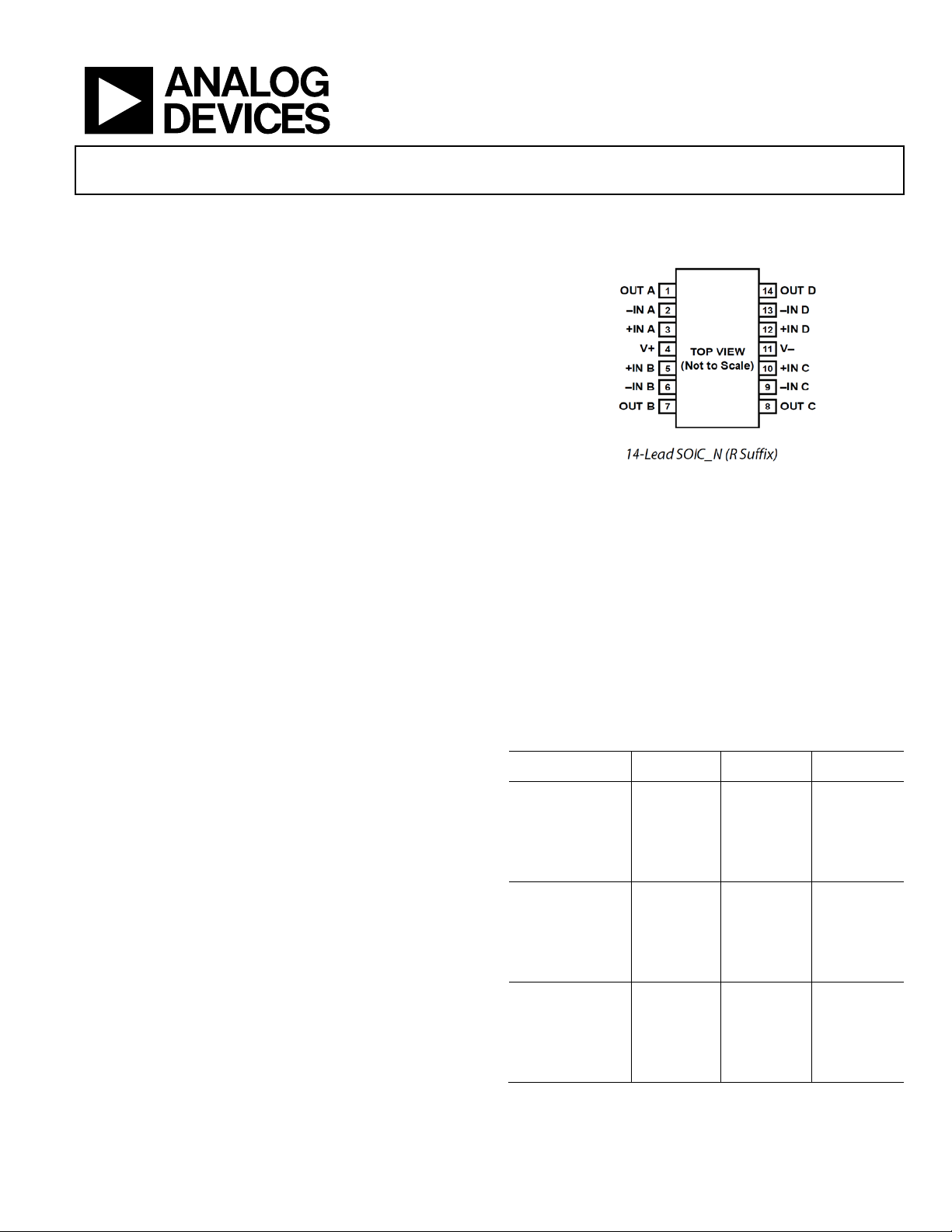
PIN CONFIGURATION
GENERAL DESCRIPTION
The AD8659 is a Quad, micropower, precision, rail-to-rail
input/output amplifier optimized for low power and wide
operating supply voltage range applications.
The AD8659 operates from 2.7 V up to 18 V with a typical
quiescent supply current of 18 μA. It uses Analog Devices, Inc.,
patented DigiTrim® trimming technique, which achieves low
offset voltage. The AD8659 also has high immunity to
electromagnetic interference.
The combination of low supply current, low offset voltage, very
low input bias current, wide supply range, and rail-to-rail input
and output make the AD8659 ideal for current monitoring and
current loops in process and motor control applications. The
combination of precision specifications makes this device ideal
for dc gain and buffering of sensor front ends or high impedance
input sources in wireless or remote sensors or transmitters.
Table 1. Micropower Op Amps
Supply Voltage 5 V 12 V to 16 V 36 V
Single AD8500 AD8663
ADA4505-1
AD8505
AD8541
Dual AD8502 AD8667 OP295
ADA4505-2 OP281 ADA4062-2
AD8542
AD8607
ADA4505-4 OP481 ADA4062-4
AD8508
AD8544
AD8609
Information furnished by Analog Devices is believed to be accurate and reliable. However, no
responsibility is assumed by Analog Devices for its use, nor for any infringements of patents or other
rights of third parties that may result from its use. Specifications subject to change without notice. No
license is granted by implication or otherwise under any patent or patent rights of Analog Devices.
One Technology Way, P.O. Box 9106, Norwood, MA 02062-9106, U.S.A.
Tel: 781.329.4700
www.analog.com

AD8659 Preliminary Technical Data
Rev. PrA | Page 2 of 8

Preliminary Technical Data AD8659
TABLE OF CONTENTS
Features ............................................................................................... 1
Applications ....................................................................................... 1
Pin Configuration ............................................................................. 1
General Description .......................................................................... 1
Revision History ........................... Error! Bookmark not defined.
Specifications ..................................................................................... 4
Electrical Characteristics—2.7 V Operation ............................. 4
Electrical Characteristics—10 V Operation .............................. 5
Electrical Characteristics—18 V Operation .............................. 6
Absolute Maximum Ratings ............................................................ 7
Thermal Resistance ....................................................................... 7
ESD Caution .................................................................................. 7
Typical Performance Characteristics .........
Applications Information ............
Input Stage ................................
Output Stage .............................
Rail to rail ..................................
Resistive load ............................
Comparator Operation............
EMI Rejection ratio .................
mA to 20 mA Process Control Current Loop Transmitter
4
....................................................
O
utline Dimensions .....................
Ordering Guide ...............................................................................
Rev. PrA | Page 3 of 8

AD8659 Preliminary Technical Data
Parameter
Symbol
Test Conditions/Comments
Min
Typ
Max
Unit
−40°C ≤ TA ≤ +125°C
500
pA
Input Resistance
RIN
10 GΩ
INDM
INCM
OUT
Supply Current per Amplifier
ISY
IO = 0 mA
18
22
µA
EMI Rejection Ratio of IN+
EMIRR
VIN = 100 mV
; f = 400 MHz, 900 MHz,
1800 MHz, 2400 MHz
90 dB
Voltage Noise
en p-p
f = 0.1 Hz to 10 Hz
6
µV p-p
SPECIFICATIONS
ELECTRICAL CHARACTERISTICS—2.7 V OPERATION
VSY = 2.7 V, VCM = V
Table 2.
INPUT CHARACTERISTICS
Offset Voltage VOS VCM = 0 V to 2.7 V 350 µV
VCM = 0.3 V to 2.4 V; −40°C ≤ TA ≤ +85°C 1 mV
VCM = 0 V to 2.7 V; −40°C ≤ TA ≤ +85°C 2.2 mV
VCM = 0.3 V to 2.4 V; −40°C ≤ TA ≤ +125°C 2.5 mV
VCM = 0 V to 2.7 V; −40°C ≤ TA ≤ +125°C 4 mV
Input Bias Current IB 1 10 pA
−40°C ≤ TA ≤ +125°C 2.6 nA
Input Offset Current IOS 20 pA
Input Voltage Range 0 2.7 V
Common-Mode Rejection Ratio CMRR VCM = 0 V to 2.7 V 79 95 dB
VCM = 0.3 V to 2.4 V; −40°C ≤ TA ≤ +85°C 70 dB
VCM = 0 V to 2.7 V; −40°C ≤ TA ≤ +85°C 64 dB
VCM = 0.3 V to 2.4 V; −40°C ≤ TA ≤ +125°C 63 dB
VCM = 0 V to 2.7 V; −40°C ≤ TA ≤ +125°C 60 dB
Large Signal Voltage Gain AVO RL = 100 kΩ, VO = 0.5 V to 2.2 V 94 105 dB
−40°C ≤ TA ≤ +85°C 75 dB
−40°C ≤ TA ≤ +125°C 65 dB
Offset Voltage Drift ΔVOS/ΔT 2 μV/°C
/2 V, T
SY
= 25°C, unless otherwise specified.
A
Input Capacitance, Differential Mode C
Input Capacitance, Common Mode C
3.5 pF
3.5 pF
OUTPUT CHARACTERISTICS
Output Voltage High VOH RL = 100 kΩ to VCM; −40°C ≤ TA ≤ +125°C 2.69 V
Output Voltage Low VOL RL = 100 kΩ to VCM; −40°C ≤ TA ≤ +125°C 10 mV
Short-Circuit Current ISC ±4 mA
Closed-Loop Output Impedance Z
f = 1 kHz, AV = 1 20 Ω
POWER SUPPLY
Power Supply Rejection Ratio PSRR VSY = 2.7 V to 18 V 105 125 dB
−40°C ≤ TA ≤ +125°C 70 dB
−40°C ≤ TA ≤ +125°C 33 µA
DYNAMIC PERFORMANCE
Slew Rate SR RL = 1 MΩ, CL = 10 p F, AV = 1 38 V/ms
Settling Time to 0.1% ts VIN = 1 V step, RL = 100 kΩ, CL = 10 pF 14 µs
Gain Bandwidth Product GBP RL = 1 MΩ, CL = 10 p F, AV = 1 170 kHz
Phase Margin ΦM RL = 1 MΩ, CL = 10 p F, AV = 1 69 Degrees
Channel Separation CS f = 10 kHz, RL = 1 MΩ 105 dB
PEAK
NOISE PERFORMANCE
Voltage Noise Density en f = 1 kHz 60 nV/√Hz
f = 10 kHz 56 nV/√Hz
Rev. PrA | Page 4 of 8

Preliminary Technical Data AD8659
Parameter
Symbol
Test Conditions/Comments
Min
Typ
Max
Unit
Input Bias Current
IB 2 15
pA
Offset Voltage Drift
ΔVOS/ΔT
2 μV/°C
INDM
INCM
Short-Circuit Current
ISC
±11 mA
OUT
−40°C ≤ TA ≤ +125°C
70
dB
DYNAMIC PERFORMANCE
Channel Separation
CS
f = 10 kHz, RL = 1 MΩ
105 dB
;
1800 MHz, 2400 MHz
NOISE PERFORMANCE
Current Noise Density in f = 1 kHz 0.1 pA/√Hz
ELECTRICAL CHARACTERISTICS—10 V OPERATION
VSY = 10 V, VCM = V
Table 3.
Parameter Symbol Test Conditions/Comments Min Typ Max Unit
INPUT CHARACTERISTICS
Offset Voltage VOS VCM = 0 V to 10 V 350 µV
VCM = 0 V to 10 V; −40°C ≤ TA ≤ +85°C 2.7 mV
VCM = 0 V to 10 V; −40°C ≤ TA ≤ +125°C 9 mV
−40°C ≤ TA ≤ +125°C 2.6 nA
Input Offset Current IOS 30 pA
−40°C ≤ TA ≤ +125°C 500 pA
Input Voltage Range 0 10 V
Common-Mode Rejection Ratio CMRR VCM = 0 V to 10 V 90 105 dB
VCM = 0 V to 10 V; −40°C ≤ TA ≤ +85°C 72 dB
VCM = 0 V to 10 V; −40°C ≤ TA ≤ +125°C 64 dB
Large Signal Voltage Gain AVO RL = 100 kΩ, VO = 0.5 V to 9.5 V 105 120 dB
−40°C ≤ TA ≤ +85°C 95 dB
−40°C ≤ TA ≤ +125°C 67 dB
/2 V, T
SY
= 25°C, unless otherwise specified.
A
Input Resistance RIN 10 GΩ
Input Capacitance, Differential Mode C
Input Capacitance, Common Mode C
3.5 pF
3.5 pF
OUTPUT CHARACTERISTICS
Output Voltage High VOH RL = 100 kΩ to VCM; −40°C ≤ TA ≤ +125°C 9.98 V
Output Voltage Low VOL RL = 100 kΩ to VCM; −40°C ≤ TA ≤ +125°C 20 mV
Closed-Loop Output Impedance Z
f = 1 kHz, AV = 1 15 Ω
POWER SUPPLY
Power Supply Rejection Ratio PSRR VSY = 2.7 V to 18 V 105 125 dB
Supply Current per Amplifier ISY IO = 0 mA 18 22 µA
−40°C ≤ TA ≤ +125°C 33 µA
Slew Rate SR RL = 1 MΩ, CL = 10 p F, AV = 1 60 V/ms
Settling Time to 0.1% ts VIN = 1 V step, RL = 100 kΩ, CL = 10 pF 13 µs
Gain Bandwidth Product GBP RL = 1 MΩ, CL = 10 pF, AV = 1 200 kHz
Phase Margin ΦM RL = 1 MΩ, CL = 10 pF, AV = 1 60 Degrees
EMI Rejection Ratio of IN+ EMIRR
VIN = 100 mV
f = 400 MHz, 900 MHz,
PEAK
90 dB
Voltage Noise en p-p f = 0.1 Hz to 10 Hz 5 µV p-p
Voltage Noise Density en f = 1 kHz 50 nV/√Hz
f = 10 kHz 45 nV/√Hz
Current Noise Density in f = 1 kHz 0.1 pA/√Hz
Rev. PrA | Page 5 of 8

AD8659 Preliminary Technical Data
Offset Voltage
VOS
VCM = 0 V to 18 V
350
µV
VCM = 0.3 V to 17.7 V; −40°C ≤ TA ≤ +85°C
83
dB
INDM
INCM
Short-Circuit Current
ISC
±12 mA
OUT
Power Supply Rejection Ratio
PSRR
VSY = 2.7 V to 18 V
105
125 dB
Phase Margin
ΦM
RL = 1 MΩ, CL = 10 p F, AV = 1
60 Degrees
;
1800 MHz, 2400 MHz
Current Noise Density
in
f = 1 kHz
0.1 pA/√Hz
ELECTRICAL CHARACTERISTICS—18 V OPERATION
VSY = 18 V, VCM = V
Table 4.
Parameter Symbol Test Conditions/Comments Min Typ Max Unit
INPUT CHARACTERISTICS
VCM = 0.3 V to 17.7 V; −40°C ≤ TA ≤ +85°C 1.2 mV
VCM = 0 V to 18 V; −40°C ≤ TA ≤ +85°C 4 mV
VCM = 0.3 V to 17.7 V; −40°C ≤ TA ≤ +125°C 2 mV
VCM = 0 V to 18 V; −40°C ≤ TA ≤ +125°C 11 mV
Input Bias Current IB 5 20 pA
−40°C ≤ TA ≤ +125°C 2.9 nA
Input Offset Current IOS 40 pA
−40°C ≤ TA ≤ +125°C 500 pA
Input Voltage Range 0 18 V
Common-Mode Rejection Ratio CMRR VCM = 0 V to 18 V 95 110 dB
VCM = 0 V to 18 V; −40°C ≤ TA ≤ +85°C 74 dB
VCM = 0.3 V to 17.7 V; −40°C ≤ TA ≤ +125°C 80 dB
VCM = 0 V to 18 V; −40°C ≤ TA ≤ +125°C 67 dB
Large Signal Voltage Gain AVO RL = 100 kΩ, VO = 0.5 V to 17.5 V 110 120 dB
−40°C ≤ TA ≤ +85°C 105 dB
−40°C ≤ TA ≤ +125°C 73 dB
Offset Voltage Drift ΔVOS/ΔT 2 μV/°C
Input Resistance RIN 10 GΩ
Input Capacitance, Differential Mode C
Input Capacitance, Common Mode C
OUTPUT CHARACTERISTICS
Output Voltage High VOH RL = 100 kΩ to VCM; −40°C ≤ TA ≤ +125°C 17.97 V
Output Voltage Low VOL RL = 100 kΩ to VCM; −40°C ≤ TA ≤ +125°C 30 mV
/2 V, T
SY
= 25°C, unless otherwise specified.
A
3.5 pF
10.5 pF
Closed-Loop Output Impedance Z
POWER SUPPLY
−40°C ≤ TA ≤ +125°C 70 dB
Supply Current per Amplifier ISY IO = 0 mA 18 22 µA
−40°C ≤ TA ≤ +125°C 33 µA
DYNAMIC PERFORMANCE
Slew Rate SR RL = 1 MΩ, CL = 10 p F, AV = 1 70 V/ms
Settling Time to 0.1% ts VIN = 1 V step, RL = 100 kΩ, CL = 10 pF 12 µs
Gain Bandwidth Product GBP RL = 1 MΩ, CL = 10 p F, AV = 1 200 kHz
Channel Separation CS f = 10 kHz, RL = 1 MΩ 105 dB
EMI Rejection Ratio of IN+ EMIRR
NOISE PERFORMANCE
Voltage Noise en p-p f = 0.1 Hz to 10 Hz 5 µV p-p
Voltage Noise Density en f = 1 kHz 50 nV/√Hz
f = 10 kHz 45 nV/√Hz
f = 1 kHz, AV = 1 15 Ω
VIN = 100 mV
Rev. PrA | Page 6 of 8
f = 400 MHz, 900 MHz,
PEAK
90 dB

Preliminary Technical Data AD8659
Input Voltage
(V−) − 300 mV to (V+) + 300 mV
ABSOLUTE MAXIMUM RATINGS
Table 4.
Parameter Rating
Supply Voltage 20.5 V
Input Current1 ±10 mA
Differential Input Voltage ±VSY
Output Short-Circuit
Duration to GND
Temperature Range
Storage −65°C to +150°C
Operating −40°C to +125°C
Junction −65°C to +150°C
Lead Temperature
(Soldering, 60 sec)
1
The input pins have clamp diodes to the power supply pins. Limit the input
current to 10 mA or less whenever input signals exceed the power supply
rail by 0.3 V.
Indefinite
300°C
Stresses above those listed under Absolute Maximum Ratings
may cause permanent damage to the device. This is a stress
rating only; functional operation of the device at these or any
other conditions above those indicated in the operational
section of this specification is not implied. Exposure to absolute
maximum rating conditions for extended periods may affect
device reliability.Thermal Resistance
is specified for the worst-case conditions, that is, a device
θ
JA
soldered in a circuit board for surface-mount packages using a
standard 4-layer board.
Table 5. Thermal Resistance
Package Type θJA θJC Unit
14-Lead SOIC (R-14) 142 45 °C/W
ESD CAUTION
Rev. PrA | Page 7 of 8

AD8659 Preliminary Technical Data
©2011 Analog Devices, Inc. All rights reserved. Trademarks and
registered trademarks are the property of their respective owners.
PR09870-0-8/11(PrA)
Rev. PrA | Page 8 of 8
 Loading...