ANALOG DEVICES AD8656 Service Manual

Low Noise,
–
A
Data Sheet
FEATURES
Low noise: 2.7 nV/√Hz @ f = 10 kHz
Low offset voltage: 250 μV max over V
Offset voltage drift: 0.4 μV/°C typ and 2.3 μV/°C max
Bandwidth: 28 MHz
Rail-to-rail input/output
Unity gain stable
2.7 V to 5.5 V operation
−40°C to +125°C operation
Qualified for automotive applications (AD8656)
APPLICATIONS
ADC and DAC buffers
Audio
Industrial controls
Precision filters
Digital scales
Automotive collision avoidance
PLL filters
GENERAL DESCRIPTION
CM
1
NC
IN
2
+IN
3
(Not to Scale)
V–
4
NC = NO CONNECT
Figure 1. AD8655
8-Lead MSOP (RM-8)
NC
1
–IN
2
3
+IN
(Not to Scale)
4
V–
NC = NO CONNECT
Figure 3. AD8655
8-Lead SOIC (R-8)
Precision CMOS Amplifier
AD8655/AD8656
PIN CONFIGURATIONS
8
AD8655
TOP VIEW
AD8655
TOP VIEW
NC
V+
7
OUT
6
NC
5
05304-048
NC
8
V+
7
6
OUT
5
NC
05304-049
1
OUT
–IN A
2
+IN A
3
V–
4
Figure 2. AD8656
8-Lead MSOP (RM-8)
OUT A
1
2
–IN A
+IN A
3
V–
4
Figure 4. AD8656
8-Lead SOIC (R-8)
AD8656
TOP VIEW
(Not to Scale)
AD8656
TOP VIEW
(Not to Scale)
8
7
6
5
8
7
6
5
V+
OUT B
–IN B
+IN B
V+
OUT B
–IN B
+IN B
05304-059
05304-060
The AD8655/AD8656 are the industry’s lowest noise, precision
CMOS amplifiers. They leverage the Analog Devices DigiTrim®
technology to achieve high dc accuracy.
The AD8655/AD8656 provide low noise (2.7 nV/√Hz @ 10 kHz),
low THD + N (0.0007%), and high precision performance
(250 μV max over V
) to low voltage applications. The ability
CM
to swing rail-to-rail at the input and output enables designers
to buffer analog-to-digital converters (ADCs) and other wide
dynamic range devices in single-supply systems.
The high precision performance of the AD8655/AD8656
improves the resolution and dynamic range in low voltage
applications. Audio applications, such as microphone pre-amps
and audio mixing consoles, benefit from the low noise, low
distortion, and high output current capability of the AD8655/
AD8656 to reduce system level noise performance and maintain
audio fidelity. The high precision and rail-to-rail input and
output of the AD8655/AD8656 benefit data acquisition, process
controls, and PLL filter applications.
The AD8655/AD8656 are fully specified over the −40°C to
+125°C temperature range. The AD8655/AD8656 are available
in Pb-free, 8-lead MSOP and SOIC packages.
Rev. B
Information furnished by Analog Devices is believed to be accurate and reliable. However, no
responsibility is assumed by Analog Devi ces for its use, nor for any infringements of patents or other
rights of third parties that may result from its use. Specifications subject to change without notice. No
license is granted by implication or otherwise under any patent or patent rights of Analog Devices.
Trademarks and registered trademarks are the property of their respective owners.
One Technology Way, P.O. Box 9106, Norwood, MA 02062-9106, U.S.A.
Tel: 781.329.4700 www.analog.com
Fax: 781.461.3113 ©2005–2011 Analog Devices, Inc. All rights reserved.

AD8655/AD8656
TABLE OF CONTENTS
Specifications..................................................................................... 3
Data Sheet
Driving Capacitive Loads.......................................................... 16
Absolute Maximum Ratings............................................................ 5
ESD Caution.................................................................................. 5
Typical Performance Characteristics............................................. 6
Theory of Operation ...................................................................... 15
Applications..................................................................................... 16
Input Overvoltage Protection................................................... 16
Input Capacitance....................................................................... 16
REVISION HISTORY
9/11—Rev. A to Rev. B
Changes to Features Section............................................................ 1
Updated Outline Dimensions....................................................... 19
Changes to Ordering Guide.......................................................... 19
Added Automotive Products Section .......................................... 19
6/05—Rev. 0 to Rev. A
Added AD8656 ...................................................................Universal
Added Figure 2 and Figure 4........................................................... 1
Changes to Specifications................................................................ 3
Changed Caption of Figure 12 and Added Figure 13.................. 7
Replaced Figure 16 ...........................................................................7
Changed Caption of Figure 37 and Added Figure 38................ 11
Replaced Figure 47 .........................................................................13
Added Figure 55.............................................................................. 14
Changes to Ordering Guide.......................................................... 18
Layout, Grounding, and Bypassing Considerations.................. 18
Power Supply Bypassing............................................................ 18
Grounding................................................................................... 18
Leakage Currents........................................................................ 18
Outline Dimensions .......................................................................19
Ordering Guide .......................................................................... 19
Automotive Products ................................................................. 19
4/05—Revision 0: Initial Version
Rev. B | Page 2 of 20

Data Sheet
AD8655/AD8656
SPECIFICATIONS
VS = 5.0 V, VCM = VS/2, TA = 25°C, unless otherwise specified.
Table 1.
Parameter Symbol Conditions Min Typ Max Unit
INPUT CHARACTERISTICS
Offset Voltage VOS V
−40°C ≤ TA ≤ +125°C 550 μV
Offset Voltage Drift
ΔV
OS
/ΔT
Input Bias Current IB 1 10 pA
−40°C ≤ TA ≤ +125°C 500 pA
Input Offset Current IOS 10 pA
−40°C ≤ TA≤ +125°C 500 pA
Input Voltage Range 0 5 V
Common-Mode Rejection Ratio CMRR VCM = 0 V to 5 V 85 100 dB
Large Signal Voltage Gain AVO V
−40°C ≤ TA ≤ +125°C 95 dB
OUTPUT CHARACTERISTICS
Output Voltage High VOH I
Output Voltage Low VOL I
Output Current I
V
OUT
POWER SUPPLY
Power Supply Rejection Ratio PSRR VS = 2.7 V to 5.0 V 88 105 dB
Supply Current/Amplifier ISY V
−40°C ≤ TA ≤ +125°C 5.3 mA
INPUT CAPACITANCE CIN
Differential 9.3 pF
Common-Mode 16.7 pF
NOISE PERFORMANCE
Input Voltage Noise Density en f = 1 kHz 4
f = 10 kHz 2.7
Total Harmonic Distortion + Noise THD + N G = 1, RL = 1 kΩ, f = 1 kHz, VIN = 2 V p-p 0.0007 %
FREQUENCY RESPONSE
Gain Bandwidth Product GBP 28 MHz
Slew Rate SR RL = 10 kΩ 11 V/μs
Settling Time ts To 0.1%, VIN = 0 V to 2 V step, G = +1 370 ns
Phase Margin CL = 0 pF 69 degrees
= 0 V to 5 V 50 250 μV
CM
−40°C ≤ T
= 0.2 V to 4.8 V, RL = 10 kΩ, VCM = 0 V 100 110 dB
O
= 1 mA; −40°C ≤ TA ≤ +125°C 4.97 4.991 V
L
= 1 mA; −40°C ≤ TA ≤ +125°C 8 30 mV
L
OUT
= 0 V 3.7 4.5 mA
O
≤ +125°C 0.4 2.3 μV/°C
A
= ±0.5 V ±220 mA
nV/√Hz
nV/√Hz
Rev. B | Page 3 of 20

AD8655/AD8656
Data Sheet
VS = 2.7 V, VCM = VS/2, TA = 25°C, unless otherwise specified.
Table 2.
Parameter Symbol Conditions Min Typ Max Unit
INPUT CHARACTERISTICS
Offset Voltage VOS V
= 0 V to 2.7 V 44 250 μV
CM
−40°C ≤ TA ≤ +125°C 550 μV
Offset Voltage Drift
ΔV
OS
/ΔT
−40°C ≤ T
≤ +125°C 0.4 2.0 μV/°C
A
Input Bias Current IB 1 10 pA
−40°C ≤ TA ≤ +125°C 500 pA
Input Offset Current IOS 10 pA
−40°C ≤ TA ≤ +125°C 500 pA
Input Voltage Range 0 2.7 V
Common-Mode Rejection Ratio CMRR VCM = 0 V to 2.7 V 80 98 dB
Large Signal Voltage Gain AVO V
= 0.2 V to 2.5 V, RL = 10 kΩ, VCM = 0 V 98 dB
O
−40°C ≤ TA ≤ +125°C 90 dB
OUTPUT CHARACTERISTICS
Output Voltage High VOH I
Output Voltage Low VOL I
Output Current I
V
OUT
= 1 mA; −40°C ≤ TA ≤ +125°C 2.67 2.688 V
L
= 1 mA; −40°C ≤ TA ≤ +125°C 10 30 mV
L
= ±0.5 V ±75 mA
OUT
POWER SUPPLY
Power Supply Rejection Ratio PSRR VS = 2.7 V to 5.0 V 88 105 dB
Supply Current/Amplifier ISY V
= 0 V 3.7 4.5 mA
O
−40°C ≤ TA ≤ +125°C 5.3 mA
INPUT CAPACITANCE CIN
Differential 9.3 pF
Common-Mode 16.7 pF
NOISE PERFORMANCE
Input Voltage Noise Density en f = 1 kHz 4.0
f = 10 kHz 2.7
nV/√Hz
nV/√Hz
Total Harmonic Distortion + Noise THD + N G = 1, RL = 1kΩ, f = 1 kHz, VIN = 2 V p-p 0.0007 %
FREQUENCY RESPONSE
Gain Bandwidth Product GBP 27 MHz
Slew Rate SR RL = 10 kΩ 8.5 V/μs
Settling Time ts To 0.1%, VIN = 0 to 1 V step, G = +1 370 ns
Phase Margin CL = 0 pF 54 degrees
Rev. B | Page 4 of 20

Data Sheet
ABSOLUTE MAXIMUM RATINGS
Table 3.
Parameter Rating
Supply Voltage 6 V
Input Voltage VSS − 0.3 V to VDD + 0.3 V
Differential Input Voltage ±6 V
Output Short-Circuit Duration
to GND
Electrostatic Discharge (HBM) 3.0 kV
Storage Temperature Range
R, RM Packages
Junction Temperature Range
R, RM Packages
Lead Temperature
(Soldering, 10 sec)
Indefinite
−65°C to +150°C
−65°C to +150°C
260°C
AD8655/AD8656
Stresses above those listed under Absolute Maximum Ratings
may cause permanent damage to the device. This is a stress
rating only; functional operation of the device at these or any
other conditions above those indicated in the operational
section of this specification is not implied. Exposure to absolute
maximum rating conditions for extended periods may affect
device reliability.
Table 4.
Package Type θ
8-Lead MSOP (RM) 210 45 °C/W
8-Lead SOIC (R) 158 43 °C/W
1
θJA is specified for worst-case conditions; that is, θJA is specified for a device
soldered in the circuit board for surface-mount packages.
1
θJC Unit
JA
ESD CAUTION
ESD (electrostatic discharge) sensitive device. Electrostatic charges as high as 4000 V readily accumulate on
the human body and test equipment and can discharge without detection. Although this product features
proprietary ESD protection circuitry, permanent damage may occur on devices subjected to high energy
electrostatic discharges. Therefore, proper ESD precautions are recommended to avoid performance
degradation or loss of functionality.
Rev. B | Page 5 of 20

AD8655/AD8656
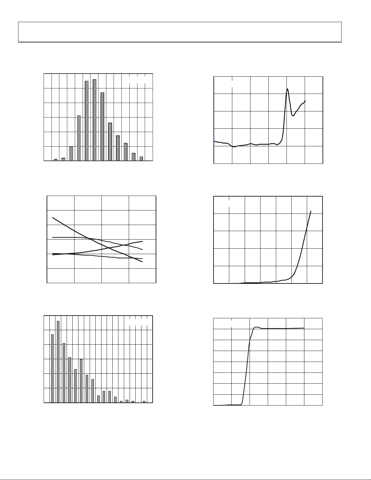
TYPICAL PERFORMANCE CHARACTERISTICS
60
VS = ±2.5V
50
40
30
20
NUMBER OF AMPLIFIERS
10
Data Sheet
20
VS = ±2.5V
10
0
(μV)
OS
V
–10
–20
0
–150 –100 –50 0 50 100 150
(μV)
V
OS
Figure 5. Input Offset Voltage Distribution
150.0
100.0
50.0
(μV)
0.0
OS
V
–50.0
–100.0
–150.0
–50 0 50
TEMPERATURE (°C)
Figure 6. Input Offset Voltage vs. Temperature
60
50
40
30
VS = ±2.5V
100 150
VS = ±2.5V
05304-001
05304-002
–30
01234
COMMON-MODE VOLTAGE (V)
Figure 8. Input Offset Voltage vs. Common-Mode Voltage
250
VS = ±2.5V
200
150
IB (pA)
100
50
0
0 20 40 60 80 100 120 140
TEMPERATURE (°C)
Figure 9. Input Bias Current vs. Temperature
4.0
VS = ±2.5V
3.5
3.0
2.5
2.0
56
05304-004
05304-005
20
NUMBER OF AMPLIFIERS
10
0
0 0.2 0.4 0.6 0.8 1.0 1.2
|TCV
Figure 7. |TC V
| (μV/°C)
OS
| Distribution
OS
1.4 1.6
05304-003
Rev. B | Page 6 of 20
1.5
SUPPLY CURRENT (mA)
1.0
0.5
0
012 34
SUPPLY VOLTAGE (V)
Figure 10. Supply Current vs. Supply Voltage
56
05304-006
 Loading...