ANALOG DEVICES AD8651, AD8652 Service Manual

50 MHz, Precision, Low Distortion,
O
www.BDTIC.com/ADI
FEATURES
Bandwidth: 50 MHz @ 5 V
Low noise: 4.5 nV/√Hz
Offset voltage: 100 μV typical, specified over
entire common-mode range
Slew rate: 41 V/μs
Rail-to-rail input and output swing
Input bias current: 1 pA
Single-supply operation: 2.7 V to 5.5 V
Space-saving MSOP and SOIC_N packaging
APPLICATIONS
Optical communications
Laser source drivers/controllers
Broadband communications
High speed ADCs and DACs
Microwave link interface
Cell phone PA control
Video line drivers
Audio
Low Noise CMOS Amplifiers
AD8651/AD8652
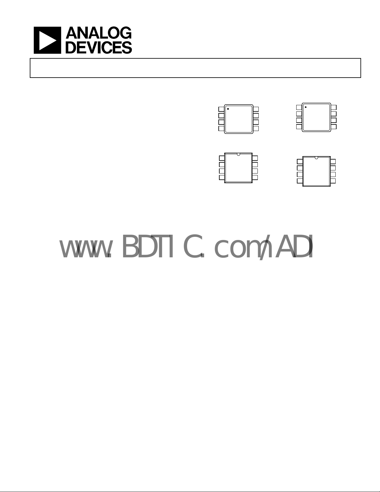
PIN CONFIGURATIONS
+
UT A
NC
1
AD8651
–IN
2
TOP VIEW
+IN
3
(Not to Scale)
–
4
V
NC = NO CONNECT
NC
8
+
7
V
OUT
6
NC
5
03301-001
–IN A
+IN A
–
V
1
AD8652
2
TOP VIEW
3
(Not to Scale)
4
Figure 1. 8-Lead MSOP (RM-8) Figure 2. 8-Lead MSOP (RM-8)
1
NC
AD8651
–IN
2
+IN
3
TOP VIEW
(Not to Scale)
–
4
V
NC = NO CONNECT
8
NC
+
7
V
OUT
6
NC
5
03301-002
OUT A
–IN A
+IN A
–
V
1
AD8652
2
3
TOP VIEW
(Not to Scale)
4
Figure 3. 8-Lead SOIC_N (R-8) Figure 4. 8-Lead SOIC_N (R-8)
8
7
6
5
8
7
6
5
V
OUT B
–IN B
+IN B
+
V
OUT B
–IN B
+IN B
03301-003
03301-004
GENERAL DESCRIPTION
The AD865x family consists of high precision, low noise, low
distortion, rail-to-rail CMOS operational amplifiers that run
from a single-supply voltage of 2.7 V to 5.5 V.
The AD865x family is made up of rail-to-rail input and output
mplifiers with a gain bandwidth of 50 MHz and a typical
a
voltage offset of 100 μV across common mode from a 5 V
supply. It also features low noise—4.5 nV/√Hz.
The AD865x family can be used in communications
ap
plications, such as cell phone transmission power control, fiber
optic networking, wireless networking, and video line drivers.
The AD865x family features the newest generation of DigiTrim®
ackage trimming. This new generation measures and
in-p
corrects the offset over the entire input common-mode range,
providing less distortion from V
variation than is typical of
OS
other rail-to-rail amplifiers. Offset voltage and CMRR are both
specified and guaranteed over the entire common-mode range
as well as over the extended industrial temperature range.
The AD865x family is offered in the narrow 8-lead SOIC
ackage and the 8-lead MSOP package. The amplifiers are
p
specified over the extended industrial temperature range
(−40°C to +125°C).
Rev. C
Information furnished by Analog Devices is believed to be accurate and reliable. However, no
responsibility is assumed by Anal og Devices for its use, nor for any infringements of patents or ot her
rights of third parties that may result from its use. Specifications subject to change without notice. No
license is granted by implication or otherwise under any patent or patent rights of Analog Devices.
Trademarks and registered trademarks are the property of their respective owners.
One Technology Way, P.O. Box 9106, Norwood, MA 02062-9106, U.S.A.
Tel: 781.329.4700 www.analog.com
Fax: 781.461.3113 ©2006 Analog Devices, Inc. All rights reserved.

AD8651/AD8652
www.BDTIC.com/ADI
TABLE OF CONTENTS
Features .............................................................................................. 1
Input Protection ..................................................................... 15
Applications....................................................................................... 1
Pin Configurations ...........................................................................1
General Description......................................................................... 1
Specifications..................................................................................... 3
Electrical Characteristics............................................................. 3
Absolute Maximum Ratings............................................................ 5
Thermal Resistance ...................................................................... 5
ESD Caution.................................................................................. 5
Typical Performance Characteristics .............................................6
Applications..................................................................................... 14
Theory of Operation ..................................................................14
Rail-to-Rail Output Stage...................................................... 14
Rail-to-Rail Input Stage......................................................... 14
REVISION HISTORY
8/06—Rev. B. to Rev. C
Changes to Figure 1 to Figure 4...................................................... 1
Changes to Figure 7 and Figure 9................................................... 6
Changes to Figure 23........................................................................ 9
Changes to Figure 53...................................................................... 14
Updated Outline Dimensions....................................................... 18
Changes to Ordering Guide.......................................................... 19
9/04—Rev. A to Rev. B
dded AD8652 ....................................................................Universal
A
Change to General Description....................................................... 1
Changes to Electrical Characteristics ............................................. 3
Changes to Absolute Maximum Ratings........................................ 5
Change to Figure 23 .......................................................................... 9
Change to Figure 26 .......................................................................... 9
Change to Figure 36 ........................................................................ 11
Change to Figure 42 ........................................................................ 12
Change to Figure 49 ........................................................................ 13
Change to Figure 51 ........................................................................ 13
Inserted Figure 52............................................................................ 13
Change to Theory of Operation section....................................... 14
Overdrive Recovery ............................................................... 15
Layout, Grounding, and Bypassing Considerations.............. 15
Power Supply Bypassing........................................................ 15
Grounding............................................................................... 15
Leakage Currents.................................................................... 15
Input Capacitance .................................................................. 16
Output Capacitance............................................................... 16
Settling Time........................................................................... 16
THD Readings vs. Common-Mode Voltage ...................... 16
Driving a 16-Bit ADC............................................................ 17
Outline Dimensions .......................................................................18
Ordering Guide .......................................................................... 19
Change to Input Protection section.............................................. 15
Changes to Ordering Guide........................................................... 20
6/04—Rev. 0 to Rev. A
C
hange to Figure 18.............................................................................8
Change to Figure 21.............................................................................9
Change to Figure 29.............................................................................10
Change to Figure 30.............................................................................10
Change to Figure 43.............................................................................12
Change to Figure 44.............................................................................12
Change to Figure 47.............................................................................13
Change to Figure 57.............................................................................17
10/03 Revision 0: Initial Version
Rev. C | Page 2 of 20

AD8651/AD8652
www.BDTIC.com/ADI
SPECIFICATIONS
ELECTRICAL CHARACTERISTICS
V+ = 2.7 V, V– = 0 V, VCM = V+/2, TA = 25°C, unless otherwise specified.
Table 1.
Parameter Symbol Conditions Min Typ Max Unit
INPUT CHARACTERISTICS
Offset Voltage V
AD8651 0 V ≤ VCM ≤ 2.7 V 100 350 V
–40°C ≤ TA ≤ +85°C, 0 V ≤ VCM ≤ 2.7 V 1.4 mV
–40°C ≤ TA ≤ +125°C, 0 V ≤ VCM ≤ 2.7 V 1.6 mV
AD8652 0 V ≤ VCM ≤ 2.7 V 90 300 V
–40°C ≤ TA ≤ +125°C, 0 V ≤ VCM ≤ 2.7 V 0.4 1.3 mV
Offset Voltage Drift TCV
Input Bias Current I
–40°C ≤ TA ≤ +125°C 600 pA
Input Offset Current I
–40°C ≤ TA ≤ +85°C 30 pA
–40°C ≤ TA ≤ +125°C 600 pA
Input Voltage Range V
Common-Mode Rejection Ratio CMRR
AD8651 V+ = 2.7 V, –0.1 V < VCM < +2.8 V 75 95 dB
–40°C ≤ TA ≤ +85°C, –0.1 V < VCM < +2.8 V 70 88 dB
–40°C ≤ TA ≤ +125°C, –0.1 V < VCM < +2.8 V 65 85 dB
AD8652 V+ = 2.7 V, –0.1 V < VCM < +2.8 V 77 95 dB
–40°C ≤ TA ≤ +125°C, –0.1 V < VCM < +2.8 V 73 90 dB
Large Signal Voltage Gain A
R
R
OUTPUT CHARACTERISTICS
Output Voltage High V
Output Voltage Low V
Short-Circuit Limit I
Sinking 80 mA
Output Current I
POWER SUPPLY
Power Supply Rejection Ratio PSRR VS = 2.7 V to 5.5 V, VCM = 0 V 76 94 dB
–40°C ≤ TA ≤ +125°C 74 93 dB
Supply Current I
AD8651 IO = 0 9 12 mA
–40°C ≤ TA ≤ +125°C 14.5 mA
AD8652 IO = 0 17.5 19.5 mA
–40°C ≤ TA ≤ +125°C 22.5 mA
INPUT CAPACITANCE C
Differential 6 pF
Common Mode 9 pF
DYNAMIC PERFORMANCE
Slew Rate SR G = 1, RL = 10 kΩ 41 V/s
Gain Bandwidth Product GBP G = 1 50 MHz
Settling Time, 0.01% G = ±1, 2 V step 0.2 s
Overload Recovery Time VIN × G = 1.48 V
Total Harmonic Distortion + Noise THD + N G = 1, RL = 600 Ω, f = 1 kHz, VIN = 2 V p-p 0.0006 %
NOISE PERFORMANCE
Voltage Noise Density e
f = 100 kHz 4.5 nV/√Hz
Current Noise Density i
OS
OS
B
OS
CM
VO
OH
OL
SC
O
SY
IN
n
n
4 V/°C
1 10 pA
1 10 pA
–0.1 +2.8 V
RL = 1 kΩ, 200 mV < VO < 2.5 V 100 115 dB
= 1 kΩ, 200 mV < VO < 2.5 V, TA = 85°C 100 114 dB
L
= 1 kΩ, 200 mV < VO < 2.5 V, TA = 125°C 95 108 dB
L
IL = 250 A, –40°C ≤ TA ≤ +125°C 2.67 V
IL = 250 A, –40°C ≤ TA ≤ +125°C 30 mV
Sourcing 80 mA
40 mA
+
f = 10 kHz 5 nV/√Hz
f = 10 kHz 4 fA/√Hz
0.1 s
Rev. C | Page 3 of 20

AD8651/AD8652
www.BDTIC.com/ADI
V+ = 5 V, V– = 0 V, VCM = V+/2, TA = 25°C, unless otherwise specified.
Table 2.
Parameter Symbol Conditions Min Typ Max Unit
INPUT CHARACTERISTICS
Offset Voltage V
AD8651 0 V ≤ VCM ≤ 5 V 100 350 V
–40°C ≤ TA ≤ +85°C, 0 V ≤ VCM ≤ 5 V 1.4 mV
–40°C ≤ TA ≤ +125°C, 0 V ≤ VCM ≤ 5 V 1.7 mV
AD8652 0 V ≤ VCM ≤ 5 V 90 300 V
–40°C ≤ TA ≤ +125°C, 0 V ≤ VCM ≤ 5 V 0.4 1.4 mV
Offset Voltage Drift TCV
Input Bias Current I
–40°C ≤ TA ≤ +85°C 30 pA
–40°C ≤ TA ≤ +125°C 600 pA
Input Offset Current I
–40°C ≤ TA ≤ +85°C 30 pA
–40°C ≤ TA ≤ +125°C 600 pA
Input Voltage Range V
Common-Mode Rejection Ratio CMRR
AD8651 0.1 V < VCM < 5.1 V 80 95 dB
–40°C ≤ TA ≤ +85°C, 0.1 V < VCM < 5.1 V 75 94 dB
–40°C ≤ TA ≤ +125°C, 0.1 V < VCM < 5.1 V 70 90 dB
AD8652 0.1 V < VCM < 5.1 V 84 100 dB
–40°C ≤ TA ≤ +125°C, 0.1 V < VCM < 5.1 V 76 95 dB
Large Signal Voltage Gain A
R
R
OUTPUT CHARACTERISTICS
Output Voltage High V
Output Voltage Low V
Short-Circuit Limit I
Sinking 80 mA
Output Current I
POWER SUPPLY
Power Supply Rejection Ratio PSRR VS = 2.7 V to 5.5 V, V
–40°C ≤ TA ≤ +125°C 74 93 dB
Supply Current I
AD8651 IO = 0 9.5 14.0 mA
–40°C ≤ TA ≤ +125°C 15 mA
AD8652 IO = 0 17.5 20.0 mA
–40°C ≤ TA ≤ +125°C 23.5 mA
INPUT CAPACITANCE C
Differential 6 pF
Common Mode 9 pF
DYNAMIC PERFORMANCE
Slew Rate SR G = 1, RL = 10 kΩ 41 V/µs
Gain Bandwidth Product GBP G = 1 50 MHz
Settling Time, 0.01% G = ±1, 2 V step 0.2 s
Overload Recovery Time VIN × G = 1.2 V
Total Harmonic Distortion + Noise THD + N G = 1, RL = 600 Ω, f = 1 kHz, VIN = 2 V p-p 0.0006 %
NOISE PERFORMANCE
Voltage Noise Density e
f = 100 kHz 4.5 nV/√Hz
Current Noise Density i
OS
OS
B
OS
CM
VO
OH
OL
SC
O
SY
IN
n
n
4 V/°C
1 10 pA
1 10 pA
–0.1 +5.1 V
RL = 1 kΩ, 200 mV < VO < 4.8 V 100 115 dB
= 1 kΩ, 200 mV < VO < 4.8 V, TA = 85°C 98 114 dB
L
= 1 kΩ, 200 mV < VO < 4.8 V, TA = 125°C 95 111 dB
L
IL = 250 µA, –40°C ≤ TA ≤ +125°C 4.97 V
IL = 250 µA, –40°C ≤ TA ≤ +125°C 30 mV
Sourcing 80 mA
40 mA
= 0 V 76 94 dB
CM
+
f = 10 kHz 5 nV/√Hz
f = 10 kHz 4 fA/√Hz
0.1 s
Rev. C | Page 4 of 20

AD8651/AD8652
www.BDTIC.com/ADI
ABSOLUTE MAXIMUM RATINGS
Absolute maximum ratings apply at 25°C, unless otherwise noted.
Table 3.
Parameter Rating
Supply Voltage 6.0 V
Input Voltage GND to V
Differential Input Voltage ±6.0 V
Output Short-Circuit Duration to GND Indefinite
Electrostatic Discharge (HBM) 4000 V
Storage Temperature Range
RM, R Package −65°C to +150°C
Operating Temperature Range −40°C to +125°C
Junction Temperature Range
RM, R Package −65°C to +150°C
Lead Temperature (Soldering, 10 sec) 300°C
Stresses above those listed under Absolute Maximum Ratings
may cause permanent damage to the device. This is a stress
rating only; functional operation of the device at these or any
other conditions above those indicated in the operational
section of this specification is not implied. Exposure to absolute
maximum rating conditions for extended periods may affect
device reliability.
+ 0.3 V
S
THERMAL RESISTANCE
JA is specified for the worst-case conditions, that is, a device
soldered in a circuit board for surface-mount packages.
Table 4. Thermal Resistance
Package Type θ
8-Lead MSOP (RM) 210 45 °C/W
8-Lead SOIC_N (R) 158 43 °C/W
JA
θ
JC
Unit
ESD CAUTION
ESD (electrostatic discharge) sensitive device. Electrostatic charges as high as 4000 V readily accumulate on
the human body and test equipment and can discharge without detection. Although this product features
proprietary ESD protection circuitry, permanent damage may occur on devices subjected to high energy
electrostatic discharges. Therefore, proper ESD precautions are recommended to avoid performance
degradation or loss of functionality.
Rev. C | Page 5 of 20

AD8651/AD8652
www.BDTIC.com/ADI
TYPICAL PERFORMANCE CHARACTERISTICS
60
50
VS = ±2.5V
V
= 0V
CM
100
VS = 5V
80
NUMBER OF AMPLIF IERS
(µV)
OS
V
–100
–200
300
200
100
40
30
20
10
0
–200
–160
–120
–80
–40
VOS (µV)
0
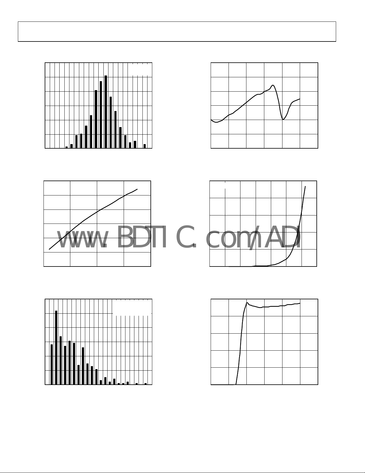
Figure 5. Input Offset Voltage Distribution
VS = ±2.5V
V
= 0V
CM
0
60
40
(µV)
OS
V
20
0
–20
40
80
120
160
200
03301-005
0123456
COMMON-MODE VOLTAGE (V)
3301-008
Figure 8. Input Offset Voltage vs. Common-Mode Voltage
500
VS = ±2.5V
400
300
200
INPUT BIAS CURRENT (pA)
100
–300
–50 0 50 100 150
TEMPERATURE (°C)
Figure 6. Input Offset Voltage vs. Temperature
60
50
40
30
20
NUMBER OF AMPLIFI ERS
10
0
01234567891011
TCVOS(µV/°C)
Figure 7. TCV
OS
VS= ±2.5V
V
T
Distribution
=0V
CM
: –40°C TO +125°C
A
0
3301-006
040 120100806020
TEMPERATURE (°C)
140
3301-009
Figure 9. Input Bias Current vs. Temperature
10
8
6
4
SUPPLY CURRENT (mA)
2
0
02 5431
3301-007
SUPPLY VOLTAGE (V)
6
3301-010
Figure 10. Supply Current vs. Supply Voltage
Rev. C | Page 6 of 20
 Loading...