

Page 1
Low Cost, 24 MHz, Rail-to-Rail,
O
O
FEATURES
Low offset voltage: 2.5 mV max
Single-supply operation: 2.7 V to 5.5 V
Low noise: 6 nV/√Hz
Wide bandwidth: 24 MHz
Slew rate: 12 V/μs
High output current: 150 mA
No phase reversal
Low input bias current: 1 pA
Low supply current: 2 mA max
Unity-gain stable
APPLICATIONS
Barcode scanners
Battery-powered instrumentation
Multipole filters
Sensors
ASIC input or output amplifiers
Audio
Photodiode amplification
GENERAL DESCRIPTION
Quad Amplifiers
AD8648
PIN CONFIGURATIONS
1
1
UT A 14
2
2
–IN A
3
3
+IN A
+IN B
–IN B
UT B
V+
AD8648
AD8648
TOP VIEW
TOP VIEW
4
4
(Not to Scale)
(Not to Scale)
5
5
6
6
7
7
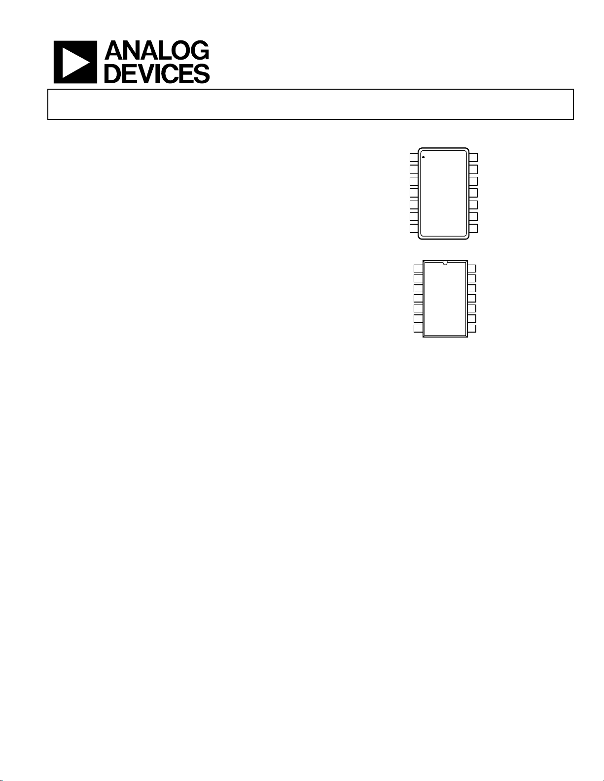
Figure 1. 14-Lead TSSOP (RU-14)
OUT A
1
1
2
2
–IN A
+IN A
3
3
AD8648
AD8648
TOP VIEW
TOP VIEW
V+
4
4
(Not to Scale)
(Not to Scale)
5
5 10
+IN B
–IN B
6
6 9
7
7 8
OUT B
Figure 2. 14-Lead SOIC (R-14)
14
14
13
13
12
12
11
11
10
14
13
13
12
12
11
11
10
10
9
9
8
8
9
8
OUT D
–IN D
+IN D
V–
+IN C
–IN C
OUT C
OUT D
–IN D
+IN D
V–
+IN C
–IN C
OUT C
05890-001
5890-002
The AD8648 is a quad, rail-to-rail, input and output, singlesupply amplifier featuring low offset voltage, wide signal
bandwidth, and low input voltage and current noise.
The combination of 24 MHz bandwidth, low offset, low noise,
and very low input bias current makes these amplifiers useful in
a wide variety of applications. Filters, integrators, photodiode
amplifiers, and high impedance sensors all benefit from the
combination of performance features. AC applications benefit
from the wide bandwidth and low distortion. The AD8648
family offers high output drive capability, which is excellent for
audio line drivers and other low impedance applications.
Applications for the part include portable and low powered
instrumentation, audio amplification for portable devices,
portable phone headsets, bar code scanners, and multipole
filters. The ability to swing rail to rail at both the input and
output enables designers to buffer CMOS ADCs, DACs, ASICs,
and other wide output swing devices in single-supply systems.
Rev. 0
Information furnished by Analog Devices is believed to be accurate and reliable. However, no
responsibility is assumed by Anal og Devices for its use, nor for any infringements of patents or ot her
rights of third parties that may result from its use. Specifications subject to change without notice. No
license is granted by implication or otherwise under any patent or patent rights of Analog Devices.
Trademarks and registered trademarks are the property of their respective owners.
One Technology Way, P.O. Box 9106, Norwood, MA 02062-9106, U.S.A.
Tel: 781.329.4700 www.analog.com
Fax: 781.461.3113 ©2006 Analog Devices, Inc. All rights reserved.
Page 2

AD8648
TABLE OF CONTENTS
Features.............................................................................................. 1
Absolute Maximum Ratings ............................................................5
Applications....................................................................................... 1
Pin Configurations ........................................................................... 1
General Description ......................................................................... 1
Revision History ............................................................................... 2
Specifications..................................................................................... 3
REVISION HISTORY
1/06—Rev 0: Initial Version
Thermal Resistance.......................................................................5
ESD Caution...................................................................................5
Typical Performance Characteristics..............................................6
Outline Dimensions....................................................................... 12
Ordering Guide .......................................................................... 12
Rev. 0 | Page 2 of 12
Page 3

AD8648
SPECIFICATIONS
VDD = 5.0 V, VCM = VDD/2, TA = 25oC, unless otherwise noted.
Table 1.
Parameter Symbol Conditions Min Typ Max Unit
INPUT CHARACTERISTICS
Offset Voltage V
OS
−40°C < TA < +125°C 3.2 mV
Offset Voltage Drift ΔVOS/ΔT −40°C < TA < +125°C 2.0 7.5 μV/°C
Input Bias Current I
B
−40°C < TA < +85°C 50 pA
−40°C < TA < +125°C 550 pA
Input Offset Current I
OS
−40°C < TA < +85°C 50 pA
−40°C < TA < +125°C 250 pA
Input Voltage Range V
CM
Common-Mode Rejection Ratio CMRR VCM = 0 V to 5.0 V 67 84 dB
Large-Signal Voltage Gain AVO R
Input Capacitance C
C
DIFF
CM
OUTPUT CHARACTERISTICS
Output Voltage High V
OH
I
−40°C < TA < +125°C 4.70 V
Output Voltage Low V
OL
I
−40°C < TA < +125°C 200 mV
Short-Circuit Output Current I
Closed-Loop Output Impedance Z
SC
OUT
POWER SUPPLY
Power Supply Rejection Ratio PSRR VDD = 2.7 V to 5.5 V 63 80 dB
Supply Current per Amplifier ISY 1.8 2.0 mA
−40°C < TA < +125°C 2.5 mA
DYNAMIC PERFORMANCE
Slew Rate SR RL = 2 kΩ 12 V/μs
Settling Time ts To 0.01% 0.5 μs
Gain Bandwidth Product GBP 24 MHz
Phase Margin Φ
M
NOISE PERFORMANCE
Peak-to-Peak Noise en p-p 0.1 Hz to 10 Hz 2.4 μV
Voltage Noise Density e
n
f = 10 kHz 6 nV/√Hz
Channel Separation CS f = 10 kHz −115 dB
f = 100 kHz −110 dB
VCM = 0 V to 5 V 0.7 2.5 mV
0.2 1 pA
0.1 0.5 pA
0 5 V
= 2 kΩ, VO = 0.5 V to 4.5 V 160 700 V/mV
L
2.5 pF
6.7 pF
I
= 1 mA 4.98 4.99 V
OUT
= 10 mA 4.87 4.92 V
OUT
I
= 1 mA 8.4 20 mV
OUT
= 10 mA 78 145 mV
OUT
±150 mA
At 1 MHz, AV = 1 3 Ω
74 Degrees
f = 1 kHz 8 nV/√Hz
Rev. 0 | Page 3 of 12
Page 4

AD8648
VDD = 2.7 V, VCM = VDD/2, TA = 25oC, unless otherwise noted.
Table 2.
Parameter Symbol Conditions Min Typ Max Unit
INPUT CHARACTERISTICS
Offset Voltage V
OS
−40°C < TA < +125°C 3.2 mV
Offset Voltage Drift ΔVOS/ΔT −40°C < TA < +125°C 1.8 7.0 μV/°C
Input Bias Current I
B
−40°C < TA < +85°C 50 pA
−40°C < TA < +125°C 550 pA
Input Offset Current I
OS
−40°C < TA < +85°C 50 pA
−40°C < TA < +125°C 250 pA
Input Voltage Range V
CM
Common-Mode Rejection Ratio CMRR VCM = 0 V to 2.7 V 62 79 dB
Large-Signal Voltage Gain AVO R
Input Capacitance C
C
DIFF
CM
OUTPUT CHARACTERISTICS
Output Voltage High V
OH
−40°C < TA < +125°C 2.60 V
Output Voltage Low V
OL
−40°C < TA < +125°C 30 mV
Short-Circuit Output Current I
Closed-Loop Output Impedance Z
SC
OUT
POWER SUPPLY
Power Supply Rejection Ratio PSRR VDD = 2.7 V to 5.5 V 63 80 dB
Supply Current per Amplifier ISY 1.7 2.0 mA
−40°C < TA < +125°C 2.5 mA
DYNAMIC PERFORMANCE
Slew Rate SR RL = 2 kΩ 12 V/μs
Settling Time ts To 0.01% 0.3 μs
Gain Bandwidth Product GBP 22 MHz
Phase Margin Φ
M
NOISE PERFORMANCE
Peak-to-Peak Noise en p-p 0.1 Hz to 10 Hz 2.1 μV
Voltage Noise Density e
n
f = 10 kHz 6 nV/√Hz
Channel Separation CS f = 10 kHz −115 dB
f = 100 kHz −110 dB
VCM = 0 V to 2.7 V 0.7 2.5 mV
0.2 1 pA
0.1 0.5 pA
0 2.7 V
= 2 kΩ, VO = 0.5 V to 2.2 V 60 130 V/mV
L
2.5 pF
7.8 pF
I
= 1 mA 2.65 2.69 V
OUT
I
= 1 mA 11 25 mV
OUT
±50 mA
At 1 MHz, AV = 1 3 Ω
52 Degrees
f = 1 kHz 8 nV/√Hz
Rev. 0 | Page 4 of 12
Page 5

AD8648
ABSOLUTE MAXIMUM RATINGS
Table 3.
Parameter Rating
Supply Voltage 6 V
Input Voltage GND to V
Differential Input Voltage ±3 V
Output Short Circuit to GND Indefinite
Storage Temperature Range −65°C to +150°C
Operating Temperature Range −40°C to +125°C
Lead Temperature (Soldering, 60 sec) 300°C
Junction Temperature 150°C
DD
Stresses above those listed under Absolute Maximum Ratings
may cause permanent damage to the device. This is a stress
rating only; functional operation of the device at these or any
other conditions above those indicated in the operational
section of this specification is not implied. Exposure to absolute
maximum rating conditions for extended periods may affect
device reliability.
THERMAL RESISTANCE
θJA is specified for the worst-case conditions, that is, a device
soldered in a circuit board for surface-mount packages.
Table 4. Thermal Resistance
Package Type θJA θ
14-Lead SOIC (R) 120 36 °C/W
14-Lead TSSOP (RU) 180 35 °C/W
Unit
JC
ESD CAUTION
ESD (electrostatic discharge) sensitive device. Electrostatic charges as high as 4000 V readily accumulate on
the human body and test equipment and can discharge without detection. Although this product features
proprietary ESD protection circuitry, permanent damage may occur on devices subjected to high energy
electrostatic discharges. Therefore, proper ESD precautions are recommended to avoid performance
degradation or loss of functionality.
Rev. 0 | Page 5 of 12
Page 6

AD8648
A
T
T
A
G
TYPICAL PERFORMANCE CHARACTERISTICS
140
120
100
VDD=5V
=2.5V
V
CM
T = 25°C
1400 AMPLIFIERS
1000
VDD=2.7VTO5V
100
80
60
40
NUMBER OF AMPLIF IERS
20
0
–2.0 –1.5 –1.0 –0.5 0 0.5 1.0 1.5 2.0
INPUT OFFSET VOLTAGE (mV)
Figure 3. Input Offset Voltage Distribution
MPLIFIERS
NUMBER OF
30
25
20
15
10
5
VDD=5V
V
=2.5V
CM
–40°C < T
< +125°C
A
10
BIAS CURRENT (pA)
1
INPU
0.1
25 45 65 85 105 125
05890-003
TE MP ERA TURE (° C)
05890-006
Figure 6. Input Bias Current vs. Temperature
1000
VDD= 5V
T = 25°C
VDD–V
E(mV)
100
10
TURATION VOLTA
S
1
OUTPU
OH
SOURCING
V
OL
SINKING
0
01234567
Figure 4. V
2500
2000
1500
1000
500
0
–500
–1000
INPUTOFFSETVOLTAGE(µV)
–1500
–2000
–2500
01234
TCVOS (µV/°C)
Drift (TCVOS) Distribution
OS
INPUT COMMON-MODE VOLTAGE (V)
VDD=5V
=25°C
T
A
Figure 5. Input Offset Voltage vs. Input Common-Mode Voltage
05890-004
5
05890-005
Rev. 0 | Page 6 of 12
0.1
0.001 0.01 0.1 1 10 100
LOAD CURRENT (mA)
Figure 7. Output Saturation Voltage vs. Load Current
25
20
15
VDD– V
OH
SOURCING
10
V
OL
SINKING
5
OUTPUT SATURAT ION VOL TAGE (mV)
0
–40 –20 0 20 40 60 80 100 120
TEMPERATURE ( °C)
VDD= 5V
I
OUT
Figure 8. Output Saturation Voltage vs. Temperature
= 1mA
05890-007
05890-008
Page 7

AD8648
(
80
60
PHASE
40
VDD = 5V
R
CL = 10pF
L
= 1k
0
Ω
45
90
100
VDD = 5V
T
= 25°C
A
80
20
0
OPEN-LOOP GAIN (dB)
–20
–40
10k 100k 1M 10M 100M
FREQUENCY (Hz)
GAIN
Ф
= 74°
M
Figure 9. Open-Loop Gain and Phase vs. Frequency
5.0
4.5
4.0
3.5
3.0
2.5
2.0
1.5
OUTPUT SWING (V p-p)
1.0
0.5
0
100k 1M 10M
FREQUENCY (Hz)
VDD = 5V
= 4.9V p-p
V
IN
= 1
A
V
= 10kΩ
R
L
= 25°C
T
A
Figure 10. Maximum Output Swing vs. Frequency
135
180
225
270
OPEN-LOOP PHASE SHIFT (Degrees)
05890-010
60
CMRR (dB)
40
20
1k 10M
05890-009
10k 100k 1M
FREQUENCY (Hz)
05890-012
Figure 12. Common-Mode Rejection Ratio vs. Frequency
100
80
60
PSRR (dB)
40
20
PSRR+
PSRR–
0
1k 10M
10k 100k 1M
FREQUENCY (Hz)
VDD = 5V
T
= 25°C
A
05890-013
Figure 13. Power Supply Rejection Ratio vs. Frequency
1000
VDD = 5V
T
= 25°C
A
100
Ω)
10
OUT
Z
1
0.1
1K 10K 100K 1M 10M 100M
AV = 100
= 10
A
V
AV = 1
FREQUENCY (Hz)
Figure 11. Closed-Loop Output Impedance vs. Frequency
05890-011
1000
100
10
VOLTAGE NOISE DENSI TY (nV/ √Hz)
1
10 10k
100 1k
FREQUENCY (Hz)
VDD = 2.7V TO 5V
= 25°C
T
A
Figure 14. Voltage Noise Density vs. Frequency
05890-014
Rev. 0 | Page 7 of 12
Page 8

AD8648
0.1
VDD = 2.7V TO 5V
= 25°C
T
A
0.01
THD + NOISE (%)
VOLTAGE (1µV/DIV)
TIME (1s/DIV)
5890-015
Figure 15. 0.1 Hz to 10 Hz Voltage Noise
VDD = 5V
R
= 10kΩ
L
C
= 20pF
L
A
= 1
V
0.001
0.0001
10020 1k
FREQUENCY (Hz)
Figure 18. THD + Noise vs. Frequency
1
0.1
VDD = 5V
= 300mV rms
V
IN
BW = 80kHz
= 100kΩ
R
L
10k 20k
05890-018
0.01
THD + NOISE (%)
0.001
0.0001
SMALL-SIGNAL OVERSHOOT (%)
VDD = 5V
= 1
A
V
BW = 30kHz
= 100kΩ
R
L
f
= 1kHz
0.010.001 0.1
OUTPUT AMPLITUDE (V rms)
Figure 19. THD + Noise vs. Output Amplitude
70
VDD = 5V
= 10kΩ
R
L
= 25°C
T
60
A
50
40
OS+
30
20
10
OS–
1
05890-019
OUTPUT VOLTAGE (50mV/DIV)
TIME (40ns/DIV)
05890-016
Figure 16. Small-Signal Transient Response
VDD = 5V
R
= 100kΩ
L
C
= 20pF
L
A
= 1
V
OUTPUT VOLTAGE (500mV/DIV)
TIME (200n s/DIV)
Figure 17. Large-Signal Transient Response
05890-017
Rev. 0 | Page 8 of 12
0
10 1000
LOAD CAPACITANCE ( pF)
100
Figure 20. Small-Signal Overshoot vs. Load Capacitance
05890-020
Page 9

AD8648
NUMBER OF AMPLIFIERS
160
140
120
100
VDD = 2.7V
= 1.35V
V
CM
T
= 25°C
A
1400 AMPLIFIERS
80
60
40
20
OUTPUT SAT URATION VO LTAGE (V)
1000
100
10
1
VDD = 2.7V
T
= 25°C
A
VDD– V
SOURCING
OH
V
OL
SINKING
0
–2.0 2.0
–1.5 –1.0 –0.5 0 0.5 1.0 1.5
INPUT OFFSET VOLTAGE (mV)
05890-021
Figure 21. Input Offset Voltage Distribution
30
25
20
15
10
NUMBER OF AMPLIFIERS
5
0
08
1234567
TCV
OS
Figure 22. V
Drift (TCVOS) Distribution
OS
(µV/°C)
VDD = 2.7V
= 1.35V
V
CM
–40°C < T
< +125° C
A
05890-022
0.1
0.001 101
Figure 24. Output Saturation Voltage vs. Load Current
25
20
15
10
5
OUTPUT SAT URATION VO LTAGE (V)
0
–40 120
–20 0 20 40 60 80 100
Figure 25. Output Saturation Voltage vs. Temperature
0.10.01
LOAD CURRENT (mA)
V
– V
DD
OH
SOURCING
TEMPERATURE (° C)
V
OL
SINKING
VDD = 2.7V
= 1mA
I
LOAD
5890-024
05890-025
2500
2000
1500
1000
500
0
–500
–1000
INPUT OFFSET VOLTAGE (µV)
–1500
–2000
–2500
03
0.5 1.0 1.5 2.0 2.5
INPUT COMMON-MODE VOLTAGE (V)
VDD = 2.7V
= 25°C
T
A
.0
05890-023
Figure 23. Input Offset Voltage vs. Input Common-Mode Voltage
80
60
40
20
0
OPEN-LOOP GAIN (dB)
–20
–40
10k 100M10M
Figure 26. Open-Loop Gain and Phase vs. Frequency
Rev. 0 | Page 9 of 12
100k 1M
FREQUENCY (Hz)
ФM = 52°
VDD = 2.7V
= 1kΩ
R
L
= 10pF
C
L
0
45
90
135
180
225
270
OPEN-LOOP PHASE SHIFT (Degrees)
5890-026
Page 10

AD8648
3.0
2.5
2.0
1.5
1.0
OUTPUT SWING (V p-p)
0.5
0
100k 1M
FREQUENCY (Hz)
Figure 27. Maximum Output Swing vs. Frequency
1000
= 2.7V
V
DD
= 25°C
T
A
100
VDD = 2.7V
= 2.6V p-p
V
IN
A
= 1
V
= 10kΩ
R
L
= 25°C
T
A
10M
5890-027
100
PSRR+
80
60
PSRR–
PSRR (dB)
40
20
0
1k 10M
10k 100k 1M
FREQUENCY (Hz)
Figure 30. Power Supply Rejection Ratio vs. Frequency
VDD = 2.7V
= 25°C
T
A
VDD = 2.7V
R
= 10kΩ
L
C
= 20pF
L
A
= 1
V
05890-030
A
= 100
V
(Ω)
10
OUT
Z
1
0.1
1k 100M
10k 100k 1M 10M
A
= 10
V
AV = 1
FREQUENCY (Hz)
Figure 28. Closed-Loop Output Impedance vs. Frequency
100
80
60
CMRR (dB)
40
VDD = 2.7V
T
= 25°C
A
OUTPUT VOLTAGE (50mV/DIV)
05890-028
TIME (40n s/DIV)
05890-031
Figure 31. Small-Signal Transient Response
VDD = 2.7V
R
= 10kΩ
L
C
= 20pF
L
A
= 1
V
OUTPUT VOLTAGE (500mV/DIV)
20
1k 10M
10k 100k 1M
FREQUENCY (Hz)
Figure 29. Common-Mode Rejection Ratio vs. Frequency
05890-029
Rev. 0 | Page 10 of 12
TIME (1µs/DIV)
Figure 32. Large-Signal Transient Response
05890-032
Page 11

AD8648
50
40
VDD = 2.7V
= 10kΩ
R
L
T
= 25°C
A
2.5
2.0
TA = 25°C
30
20
10
SMALL-SIGNAL OVERSHOOT (%)
0
1 1000
10 100
LOAD CAPACITANCE ( pF)
OS+
OS–
Figure 33. Small-Signal Overshoot vs. Load Capacitance
4.0
3.5
3.0
2.5
2.0
1.5
1.0
V
VDD = 2.7V
VDD = 5.0V
OUT
= VDD/2
1.5
1.0
0.5
SUPPLY CURRENT PER AMPLIFIER (mA)
0
05
0.5 1.0 1.5 2.0 2. 5 3.0 3.5 4.0 4. 5
05890-033
SUPPLY VOLTAGE (V)
.0
05890-035
Figure 35. Supply Current per Amplifier vs. Supply Voltage
0.5
SUPPLY CURRENT PER AMPLIFIER (mA)
0
–40 120
–20 0 20 40 60 80 100
TEMPERATURE (° C)
05890-034
Figure 34. Supply Current per Amplifier vs. Temperature
Rev. 0 | Page 11 of 12
Page 12

AD8648
OUTLINE DIMENSIONS
5.10
5.00
4.90
4.50
4.40
4.30
PIN 1
1.05
1.00
0.80
0.15
0.05
4.00 (0.1575)
3.80 (0.1496)
0.25 (0.0098)
0.10 (0.0039)
COPLANARITY
0.10
14
0.65
BSC
0.30
0.19
COMPLIANT TO JEDEC STANDARDS MO-153-AB-1
8
6.40
BSC
71
1.20
MAX
SEATING
PLANE
0.20
0.09
COPLANARITY
0.10
8°
0°
Figure 36. 14-Lead Thin Shrink Small Outline Package [TSSOP]
(RU-14)
Dimensions shown in millimeters
8.75 (0.3445)
8.55 (0.3366)
14
1
1.27 (0.0500)
BSC
0.51 (0.0201)
0.31 (0.0122)
8
6.20 (0.2441)
7
5.80 (0.2283)
1.75 (0.0689)
1.35 (0.0531)
SEATING
PLANE
0.25 (0.0098)
0.17 (0.0067)
0.50 (0.0197)
0.25 (0.0098)
8°
0°
1.27 (0.0500)
0.40 (0.0157)
0.75
0.60
0.45
× 45°
COMPLIANT TO JEDEC STANDARDS MS-012-AB
CONTROLLING DIMENSIONS ARE IN MILLIMETERS; INCH DIMENSIONS
(IN PARENTHESES) ARE ROUNDED-OFF MILLIMETER EQUIVALENTS FOR
REFERENCE ONLY AND ARE NOT APPROPRIATE FOR USE IN DESIGN.
Figure 37. 14-Lead Standard Small Outline Package [SOIC_N]
Narrow Body (R-14)
Dimensions shown in millimeters and (inches)
ORDERING GUIDE
Model Temperature Range Package Description Package Option
AD8648ARZ
AD8648ARZ-REEL
AD8648ARZ-REEL7
AD8648ARUZ
AD8648ARUZ-REEL
1
Z = Pb-free part.
©2006 Analog Devices, Inc. All rights reserved. Trademarks and
registered trademarks are the property of their respective owners.
D05890–0–1/06(0)
1
1
1
1
1
−40°C to +125°C 14-Lead SOIC_N R-14
−40°C to +125°C 14-Lead SOIC_N R-14
−40°C to +125°C 14-Lead SOIC_N R-14
−40°C to +125°C 14-Lead TSSOP RU-14
−40°C to +125°C 14-Lead TSSOP RU-14
Rev. 0 | Page 12 of 12
 Loading...