

Single and Quad 18 V
www.BDTIC.com/ADI
FEATURES
Unity-gain bandwidth: 5.5 MHz
Low voltage offset: 1.0 mV
Slew rate: 7.5 V/μs
Single-supply operation: 5 V to 18 V
High output current: 70 mA
Low supply current: 800 μA/amplifier
Stable with large capacitive loads
Rail-to-rail inputs and outputs
APPLICATIONS
LCD gamma and V
Modems
Portable instrumentation
Direct access arrangement
GENERAL DESCRIPTION
The AD8614 (single) and AD8644 (quad) are single-supply,
5.5 MHz bandwidth, rail-to-rail amplifiers optimized for LCD
monitor applications.
They are processed using the Analog Devices, Inc. high voltage,
extra fas
proprietary process includes trench-isolated transistors that
lower internal parasitic capacitance, which improves gain
bandwidth, phase margin, and capacitive load drive. The low
supply current of 800 μA (typical) per amplifier is critical for
portable or densely packed designs. In addition, the rail-to-rail
output swing provides greater dynamic range and control than
standard video amplifiers provide.
These products operate from supplies of 5 V to as high as 18 V.
T
slew rates, and high capacitive drive capability makes the
AD8614/AD8644 an ideal choice for LCD applications.
The AD8614 and AD8644 are specified over the temperature
ra
14-lead TSSOP, and 14-lead SOIC surface-mount packages in
tape and reel.
t complementary bipolar (HV XFCB) process. This
he unique combination of an output drive of 70 mA, high
nge of –20°C to +85°C. They are available in 5-lead SOT-23,
COM
drivers
Operational Amplifiers
AD8614/AD8644
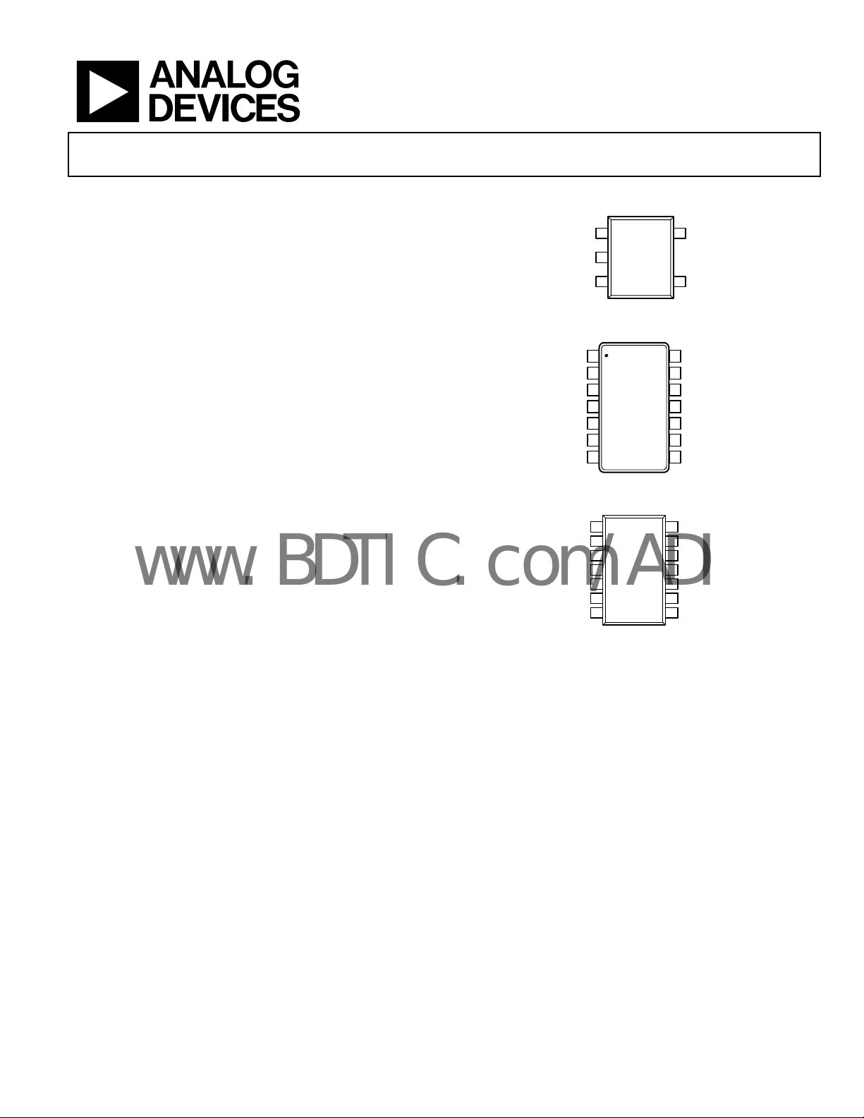
PIN CONFIGURATIONS
1
OUT A
V–
+IN
AD8614
2
TOP VIEW
(Not to Scale)
3
Figure 1. 5-Lead SOT-23
(RJ-5)
1
OUT A
2
–IN A
3
V+
AD8644
TOP VIEW
4
(Not to Scale)
5
6
7
+IN A
+IN B
–IN B
OUT B
Figure 2. 14-Lead TSSOP
(R
U-14)
OUT A
1
–IN A
2
+IN A
3
AD8644
TOP VIEW
4
V+
(Not to Scale)
5
+IN B
–IN B
6
OUT B
7
Figure 3. 14-Lead Narrow Body SOIC
(R
-14)
14
13
12
11
10
14
13
12
11
10
9
8
9
8
V+
5
4
–IN
OUT D
–IN D
+IN D
V–
+IN C
–IN C
OUT C
OUT D
–IN D
+IN D
V–
+IN C
–IN C
OUT C
06485-001
6485-002
06485-003
Rev. B
Information furnished by Analog Devices is believed to be accurate and reliable. However, no
responsibility is assumed by Anal og Devices for its use, nor for any infringements of patents or ot her
rights of third parties that may result from its use. Specifications subject to change without notice. No
license is granted by implication or otherwise under any patent or patent rights of Analog Devices.
Trademarks and registered trademarks are the property of their respective owners.
One Technology Way, P.O. Box 9106, Norwood, MA 02062-9106, U.S.A.
Tel: 781.329.4700 www.analog.com
Fax: 781.461.3113 ©1999–2007 Analog Devices, Inc. All rights reserved.

AD8614/AD8644
www.BDTIC.com/ADI
TABLE OF CONTENTS
Features.............................................................................................. 1
Applications....................................................................................... 1
General Description ......................................................................... 1
Pin Configurations ........................................................................... 1
Revision History ............................................................................... 2
Specifications..................................................................................... 3
Electrical Characteristics ............................................................. 3
Absolute Maximum Ratings............................................................ 4
Thermal Resistance ...................................................................... 4
ESD Caution.................................................................................. 4
Typical Performance Characteristics ............................................. 5
Theory of Operation ........................................................................ 9
REVISION HISTORY
9/07—Rev. A to Rev B
Change to Current Noise Density in Table 1 ................................ 3
12/06—Rev. 0 to Rev. A
Updated Format..................................................................Universal
Deleted SPICE Model Availability Section.................................. 12
Updated Outline Dimensions....................................................... 13
Changes to Ordering Guide.......................................................... 14
10/99—Revision 0: Initial Version
Output Short-Circuit Protection.................................................9
Input Overvoltage Protection................................................... 10
Output Phase Reversal............................................................... 10
Power Dissipation....................................................................... 10
Unused Amplifiers ..................................................................... 10
Capacitive Load Drive ............................................................... 11
Direct Access Arrangement...................................................... 11
A One-Chip Headphone/Microphone Preamplifier
Solution........................................................................................ 11
Outline Dimensions....................................................................... 13
Ordering Guide .......................................................................... 14
Rev. B | Page 2 of 16

AD8614/AD8644
www.BDTIC.com/ADI
SPECIFICATIONS
ELECTRICAL CHARACTERISTICS
5 V ≤ VS ≤ 18 V, VCM = VS/2, TA = 25°C, unless otherwise noted.
Table 1.
Parameter Symbol Conditions Min Typ Max Unit
INPUT CHARACTERISTICS
Offset Voltage VOS 1.0 2.5 mV
−20°C ≤ TA ≤ +85°C 3 mV
Input Bias Current IB 80 400 nA
−20°C ≤ TA ≤ +85°C 500 nA
Input Offset Current IOS 5 100 nA
−20°C ≤ TA ≤ +85°C 200 nA
Input Voltage Range 0 VS V
Common-Mode Rejection Ratio CMRR VCM = 0 V to VS 60 75 dB
Voltage Gain AVO V
OUTPUT CHARACTERISTICS
Output Voltage High VOH I
Output Voltage Low VOL I
Output Short-Circuit Current ISC 35 70 mA
−20°C ≤ TA ≤ +85°C 30 mA
POWER SUPPLY
Power Supply Rejection Ratio PSRR VS = ±2.25 V to ±9.25 V 80 110 dB
Supply Current/Amplifier ISY 0.8 1.1 mA
−20°C ≤ TA ≤ +85°C 1.5 mA
DYNAMIC PERFORMANCE
Slew Rate SR CL = 200 pF 7.5 V/μs
Gain Bandwidth Product GBP 5.5 MHz
Phase Margin Φo 65 Degrees
Settling Time tS 0.01%, 10 V step 3 μs
NOISE PERFORMANCE
Voltage Noise Density en f = 1 kHz 12 nV/√Hz
e
Current Noise Density in f = 10 kHz 1 pA/√Hz
1
All typical values are for VS = 18 V.
f = 10 kHz 11 nV/√Hz
n
OUT
LOAD
LOAD
1
= 0.5 V to VS – 0.5 V, RL = 10 kΩ 10 150 V/mV
= 10 mA VS − 0.15 V
= 10 mA 65 150 mV
Rev. B | Page 3 of 16
AD8614/AD8644
www.BDTIC.com/ADI
ABSOLUTE MAXIMUM RATINGS
Table 2.
Parameter Rating
Supply Voltage 20 V
Input Voltage GND to VS
Storage Temperature Range −65°C to +150°C
Operating Temperature Range −20°C to +85°C
Junction Temperature Range −65°C to +150°C
Lead Temperature Range (Soldering, 60 sec) 300°C
Stresses above those listed under Absolute Maximum Ratings
may cause permanent damage to the device. This is a stress
rating only; functional operation of the device at these or any
other conditions above those indicated in the operational
section of this specification is not implied. Exposure to absolute
maximum rating conditions for extended periods may affect
device reliability.
THERMAL RESISTANCE
θJA is specified for the worst-case conditions, that is, a device
soldered in a circuit board for surface-mount packages.
Table 3. Thermal Resistance
Package Type θJA θ
5-Lead SOT-23 (RJ) 230 140 °C/W
14-Lead TSSOP (RU) 180 35 °C/W
14-Lead SOIC (R) 120 56 °C/W
Unit
JC
ESD CAUTION
Rev. B | Page 4 of 16
AD8614/AD8644
www.BDTIC.com/ADI
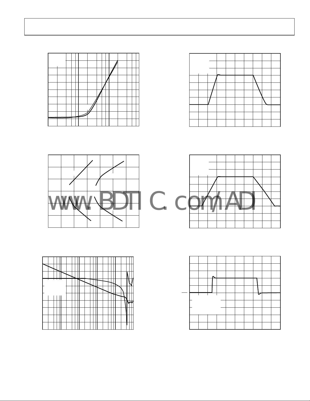
TYPICAL PERFORMANCE CHARACTERISTICS
50
VS=18V
R
=2kΩ
45
L
T
=25°C
A
40
35
30
25
20
15
10
SMALL SIGNAL OVERSHOOT (%)
5
0
10 100 1k 10k
+OS
–OS
CAPACITANCE (p F)
Figure 4. Small Signal Overshoot vs. Load Capacitance
06485-004
7.5
VS=5V
R
=2kΩ
6.5
L
C
=200pF
L
A
=1
V
5.5
T
=25°C
A
4.5
3.5
2.5
1.5
VOLTAGE (1V/DIV)
0.5
–0.5
–1.5
–2.5
TIME (1µs/DIV)
Figure 7. Large Signal Transient Response, V
= 5 V
S
06485-007
12
8
0.1%
4
0
–4
OUTPUT SWING FROM 0 TO ±V
–8
–12
0 0.5 1.0 1.5 2.0 2.5 3.0 3.5
0.1%
SETTLING TIME (µs)
0.01%
0.01%
Figure 5. Output Swing vs. Settling Time
80
60
40
5V ≤ VS≤ 18V
=1MΩ
R
20
L
=40pF
C
L
= 25°C
T
0
A
GAIN (dB)
45
90
135
180
29
VS=18V
R
=2kΩ
25
L
C
=200pF
L
A
=1
V
21
T
= 25°C
A
17
13
9
5
VOLTAGE (4V/DIV)
1
–3
–7
06485-005
–11
TIME (1µs/DIV)
06485-008
PHASE SHIFT (Degrees)
Figure 8. Large Signal Transient Response, V
V
S
2
VS=5V≤ VS≤ 18V
R
=2kΩ
L
C
= 200pF
A
T
L
=1
V
= 25°C
A
VOLTAGE (50mV/DIV)
= 18 V
S
1k 10k 100k 1M 10M 100M
FREQUENCY ( Hz)
Figure 6. Open-Loop Gain and Phase Shift vs. Frequency
06485-006
Figure 9. Small Signal Transient Response
Rev. B | Page 5 of 16
TIME (500ns/DIV)
06485-009
AD8614/AD8644
www.BDTIC.com/ADI
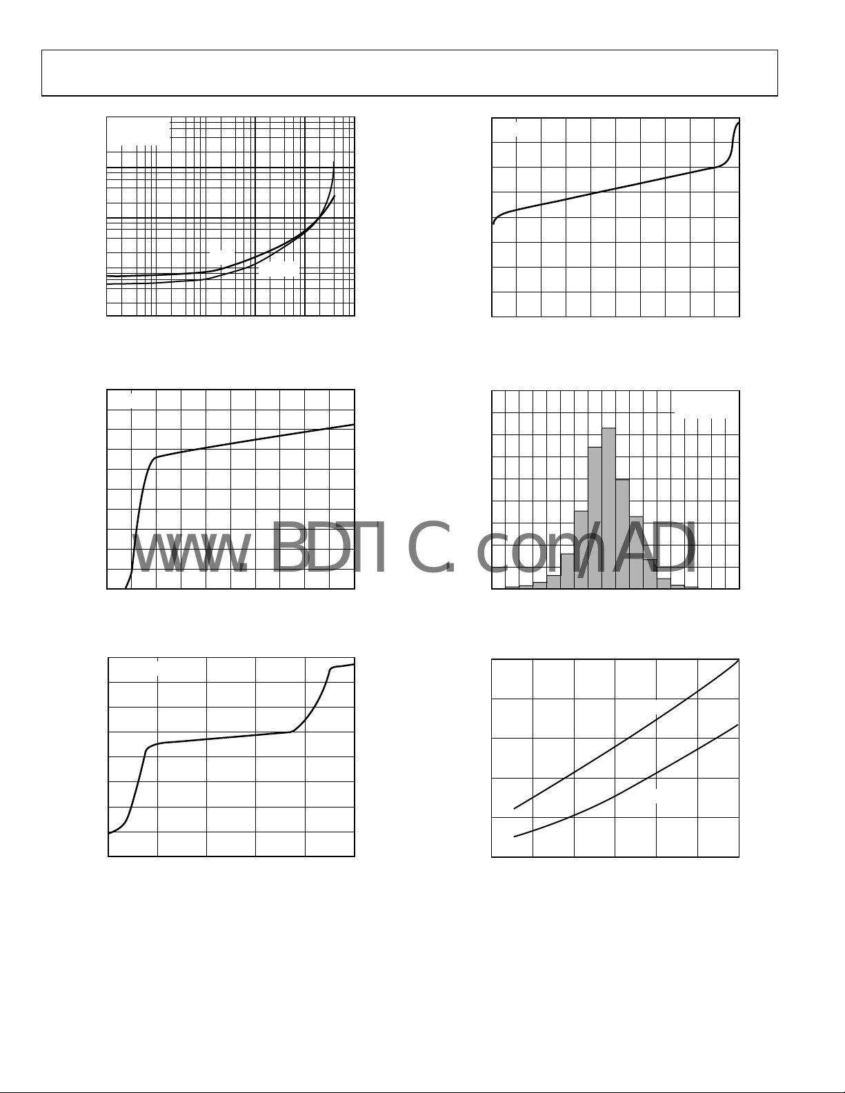
10k
5V ≤ VS≤ 18V
=25°C
T
A
400
300
VS=±9V
1k
100
ΔOUTPUT VOLTAGE (mV)
10
1
0.001 0.01 0.1 1 10 100
SINK
SOURCE
LOAD CURRENT (mA)
Figure 10. Output Voltage to Supply Rail vs. Load Current
1000
TA= 25°C
900
800
700
600
500
400
300
200
SUPPLY CURRENT/AMP LIFIER (µA)
100
0
012345678910
SUPPLY VOLTAGE (±V)
Figure 11. Supply Current vs. Supply Voltage
200
100
0
–100
–200
INPUT BIAS CURRENT (nA)
–300
06485-010
–400
–9–7–5–3–1013579
COMMON-MODE VOLTAGE (V)
Figure 13. Input Bias Current vs. Common-Mode Voltage, V
180
160
140
120
100
80
60
QUANTITY (Amplifiers)
40
20
06485-011
0
INPUT OFFSET VOLTAGE (mV)
2.5V ≤ VS≤ 9V
T
= 25°C
A
= ±9 V
S
2.01.51.00.50–0.5–1.0–1.5–2.0
06485-013
06485-014
Figure 14. Input Offset Voltage Distribution
400
VS= ±2.5V
300
200
100
0
–100
–200
INPUT BIAS CURRENT (nA)
–300
–400
–2.5 –1. 5 –0.5 0. 5 1.5 2.5
COMMON-MO DE VOLT AGE (V)
Figure 12. Input Bias Current vs. Common-Mode Voltage, V
= ±2.5 V
S
06485-012
Rev. B | Page 6 of 16
1.0
0.9
0.8
0.7
0.6
SUPPLY CURRENT/ AMPLIFI ER (mA)
0.5
–35 –15 5 25 45 65 85
TEMPERATURE (°C)
VS=18V
VS=5V
Figure 15. Supply Current vs. Temperature
06485-015

AD8614/AD8644
www.BDTIC.com/ADI
6
5
VS=5V
A
=1
VCL
R
=2kΩ
L
4
T
= 25°C
A
3
2
OUTPUT SWING (V p-p)
1
GAIN (dB)
5V ≤ VS≤ 18V
T
A
40
20
0
=25°C
0
100 1k 10k 100k 1M 10M
FREQUENCY (Hz)
Figure 16. Maximum Output Swing vs. Frequency, V
20
18
VS= 18V
16
A
=1
VCL
R
=2kΩ
L
T
14
12
10
8
6
OUTPUT SWING (V p-p)
4
2
0
100 1k 10k 100k 1M 10M
= 25°C
A
FREQUENCY (Hz)
Figure 17. Maximum Output Swing vs. Frequency, V
300
5V ≤ VS≤ 18V
T
=25°C
A
240
= 5 V
S
= 18 V
S
06485-016
1k 10k 100k 1M 10M 100M
FREQUENCY (Hz)
06485-019
Figure 19. Closed-Loop Gain vs. Frequency
140
5V ≤ VS≤ 18V
=25°C
T
A
120
100
80
60
40
COMMON-MO DE REJECTIO N (dB)
20
06485-017
0
100 1k 10k 100k 1M 10M
FREQUENCY (Hz)
06485-020
Figure 20. Common-Mode Rejection vs. Frequency
100
80
VS= 18V
= 25°C
T
A
180
120
IMPEDANCE (Ω)
60
AV=100
0
1k 10k 100k 1M 10M
Figure 18. Closed-Loop Outpu
AV=10
FREQUENCY ( Hz)
t Impedance vs. Frequency
AV=1
06485-018
60
40
20
POWER SUPPL Y REJECTION (dB)
0
Figure 21. Power Supply R
Rev. B | Page 7 of 16
FREQUENCY ( Hz)
ejection vs. Frequency
PSRR+
PSRR–
06485-021
10M1M100k10k1k100

AD8614/AD8644
www.BDTIC.com/ADI
9
8
7
6
5
4
3
SLEW RATE (V/µs)
2
AV=1
=2kΩ
R
L
1
= 200pF
C
L
= 25°C
T
A
0
02468101214161820
SUPPLY VOLTAGE (V)
SR+
SR–
Figure 22. Slew Rate vs. Supply Voltage
100
10
VS=5V
T
=25°C
A
06485-022
100
10
VOLTAGE NOISE DENSITY (nV/ Hz)
1
10 100 1k 10k
FREQUENCY (Hz)
Figure 24. Voltage Noise Density vs. Frequency, V
VS= 18V
T
A
= 18 V
S
= 25°C
06485-024
VOLTAGE NOISE DENSI TY (nV/ Hz)
1
10 100 1k 10k
FREQUENCY (Hz)
Figure 23. Voltage Noise Density vs. Frequency, V
= 5 V
S
06485-023
Rev. B | Page 8 of 16
AD8614/AD8644
V
V
www.BDTIC.com/ADI
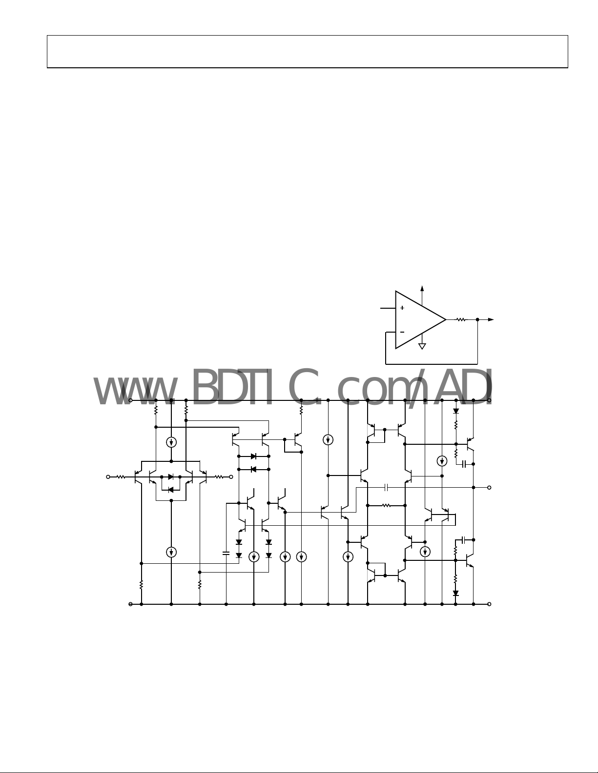
THEORY OF OPERATION
The AD8614/AD8644 are processed using Analog Devices high
voltage, extra fast complementary bipolar (HV XFCB) process.
This process includes trench-isolated transistors that lower
parasitic capacitance.
Figure 26 shows a simplified schematic of the AD8614/AD8644.
he input stage is rail-to-rail, consisting of two complementary
T
differential pairs, one NPN pair and one PNP pair. The input
stage is protected against avalanche breakdown by two back-toback diodes. Each input has a 1.5 kΩ resistor that limits input
current during overvoltage events and furnishes phase reversal
protection if the inputs are exceeded. The two differential pairs
are connected to a double-folded cascode. This is the stage in
the amplifier with the most gain. The double-folded cascode
differentially feeds the output stage circuitry. Two complementary common emitter transistors are used as the output stage.
This allows the output to swing to within 125 mV from each rail
with a 10 mA load. The gain of the output stage, and thus the
open-loop gain of the op amp, depends on the load resistance.
The AD8614/AD8644 have no built-in short-circuit protection.
The sh
ort-circuit limit is a function of high current roll-off of
the output stage transistors and the voltage drop over the
resistor shown on the schematic at the output stage. The voltage
over this resistor is clamped to one diode during short-circuit
voltage events.
OUTPUT SHORT-CIRCUIT PROTECTION
To achieve a wide bandwidth and high slew rate, the output of
the AD8614/AD8644 is not short-circuit protected. Shorting
the output directly to ground or to a supply rail can destroy the
device. The typical maximum safe output current is 70 mA.
In applications where some output current protection is needed,
b
ut not at the expense of reduced output voltage headroom, a
low value resistor in series with the output can be used. This is
shown in
edback loop of the amplifier so that if V
fe
ground and V
exceed 70 mA.
For 18 V single-supply applications, resistors less than 261 Ω are
not
Figure 25. The resistor is connected within the
OUT
swings up to 18 V, the output current does not
IN
recommended.
18
V
IN
AD86x4
Figure 25. Output Short-Circuit Protection
261Ω
is shorted to
V
OUT
06485-026
CC
– +
1.5kΩ
V
EE
1.5kΩ
V
V
CC
CC
Figure 26. Simplifi
ed Schematic
V
OUT
06485-025
Rev. B | Page 9 of 16

AD8614/AD8644
www.BDTIC.com/ADI
INPUT OVERVOLTAGE PROTECTION
As with any semiconductor device, whenever the condition
exists for the input to exceed either supply voltage, attention
needs to be paid to the input overvoltage characteristic. As an
overvoltage occurs, the amplifier can be damaged, depending
on the voltage level and the magnitude of the fault current.
When the input voltage exceeds either supply by more than
0.6 V, internal pin junctions energize, allowing current to flow
from the input to the supplies. Observing
AD8614/AD86
44 have 1.5 kΩ resistors in series with each
Figure 26, the
input, which helps to limit the current. This input current is not
inherently damaging to the device as long as it is limited to
5 mA or less. If the voltage is large enough to cause more than
5 mA of current to flow, an external series resistor should be
added. The size of this resistor is calculated by dividing the
maximum overvoltage by 5 mA and subtracting the internal
1.5 kΩ resistor. For example, if the input voltage could reach 100 V,
the external resistor should be (100 V ÷ 5 mA) – 1.5 kΩ = 18.5 kΩ.
This resistance should be placed in series with either or both
inputs if they are subjected to the overvoltages.
OUTPUT PHASE REVERSAL
The AD8614/AD8644 are immune to phase reversal as long as
the input voltage is limited to within the supply rails. Although
the device’s output does not change phase, large currents due to
input overvoltage can result, damaging the device. In applications where the possibility of an input voltage exceeding the
supply voltage exists, overvoltage protection should be used, as
described in the previous section.
POWER DISSIPATION
The maximum power that can be safely dissipated by the
AD8614/AD8644 is limited by the associated rise in junction
temperature. The maximum safe junction temperature is 150°C,
and should not be exceeded or device performance could suffer.
If this maximum is momentarily exceeded, proper circuit
operation is restored as soon as the die temperature is reduced.
Leaving the device in an overheated condition for an extended
period can result in permanent damage to the device.
To calculate the internal junction temperature of the
AD8614/AD86
= P
T
J
44, the following formula can be used:
× θJA + TA
DISS
where:
T
is the AD8614/AD8644 junction temperature.
J
P
is the AD8614/AD8644 power dissipation.
DISS
is the AD8614/AD8644 junction-to-ambient package thermal
θ
JA
resistance.
T
is the ambient temperature of the circuit.
A
The power dissipated by the device can be calculated as:
P
= I
DISS
LOAD
× (VS – V
OUT
)
where:
I
is the AD8614/AD8644 output load current.
LOAD
V
is the AD8614/AD8644 supply voltage.
S
is the AD8614/AD8644 output voltage.
V
OUT
Figure 27 provides a convenient way to determine if the device
eing overheated. The maximum safe power dissipation can
is b
be found graphically, based on the package type and the ambient
temperature around the package. By using the previous equation, it
is a simple matter to see if P
exceeds the device’s power derating
DISS
curve. To ensure proper operation, it is important to observe the
recommended derating curves shown in
1.5
14-LEAD SOI C PACKAGE
θ
= 120°C/W
JA
1.0
14-LEAD TSSOP PACKAGE
θ
= 180°C/W
JA
0.5
5-LEAD SOT-23 PACKAGE
θ
= 230°C/W
JA
MAXIMUM POWER DISSIPATION (W)
0
–35–15 5 25456585
Figure 27. Maximum Power Dissipation vs. Temperature
AMBIENT T EMPERATURE (°C)
(5-Lead
and 14-Lead Package Types)
Figure 27.
06485-027
UNUSED AMPLIFIERS
It is recommended that any unused amplifiers in the quad
package be configured as a unity-gain follower with a 1 kΩ
feedback resistor connected from the inverting input to the
output, and the noninverting input tied to the ground plane.
Rev. B | Page 10 of 16

AD8614/AD8644
V
V
www.BDTIC.com/ADI
CAPACITIVE LOAD DRIVE
The AD8614/AD8644 exhibit excellent capacitive load driving
capabilities. Although the device is stable with large capacitive
loads, there is a decrease in amplifier bandwidth as the
capacitive load increases.
When driving heavy capacitive loads directly from the
AD8614/AD86
improve the transient response. This network consists of a
series R-C connected from the amplifier’s output to ground,
placing it in parallel with the capacitive load. The configuration
is shown in
he bandwidth of the amplifier, it does significantly reduce the
t
amount of overshoot.
Figure 28. Snubber Network Compen
The optimum values for the snubber network should be
determined empirically based on the size of the capacitive load.
Tabl e 4 shows a few sample snubber network values for a given
ad capacitance.
lo
Table 4. Snubber Networks for Large Capacitive Loads
Load Capacitance (CL) Snubber Network (RX, CX)
0.47 nF 300 Ω, 0.1 μF
4.7 nF 30 Ω, 1 μF
47 nF 5 Ω, 10 μF
44 output, a snubber network can be used to
Figure 28. Although this network does not increase
5V
V
AD86x4
IN
R
X
C
X
sation for Capacitive Loads
OUT
C
L
06485-028
P1
Tx GAIN
TO TELEPHONE
LINE
1:1
Z
O
600Ω
T1
MIDCOM
671-8005
A1, A2 = 1/2 AD8644
A3, A4 = 1/2 AD8644
6.2V
6.2V
R11
10kΩ
360Ω
R9
10kΩ
R12
10kΩ
ADJUST
R3
R5
10kΩ
R6
10kΩ
R10
10kΩ
2
A3
3
2kΩ
R2
9.09kΩ
2
1
A1
3
6
7
A2
5
R13
10kΩ
1
14.3kΩ
6
5
R14
R1
10kΩ
A4
C1
0.1µF
5V DC
10µF
P2
Rx GAIN
ADJUST
2kΩ
7
C2
0.1µF
TRANSMIT
R7
10kΩ
R8
10kΩ
RECEIVE
TxA
RxA
Figure 29. A Single-Supply Direct Access Arrangement for Modems
A ONE-CHIP HEADPHONE/MICROPHONE PREAMPLIFIER SOLUTION
Because of its high output current performance, the AD8644
makes an excellent amplifier for driving an audio output jack in
a computer application. Figure 30 shows how the AD8644 can
b
e interfaced with an ac codec to drive headphones or speakers.
5
AV
DD1
VREFOUT
LINE_OUT_L
AD1881A
(AC'97)
25
28
35
5V
10
2
U1-A
1
4
3
5
C1
100µF
+
2kΩ
R3
20Ω
R1
06485-029
DIRECT ACCESS ARRANGEMENT
Figure 29 shows a schematic for a 5 V single-supply transmit/
receive telephone line interface for 600 Ω transmission systems. It
allows full duplex transmission of signals on a transformercoupled 600 Ω line. Amplifier A1 provides gain that can be
adjusted to meet the modem’s output drive requirements. Both
A1 and A2 are configured to apply the largest possible differential
signal to the transformer. The largest signal available on a single
5 V supply is approximately 4.0 V p-p into a 600 Ω transmission
system. Amplifier A3 is configured as a difference amplifier to
extract the receive information from the transmission line for
amplification by A4. A3 also prevents the transmit signal from
interfering with the receive signal. The gain of A4 can be adjusted
in the same manner as A1 to meet the modem input signal
requirements. Standard resistor values permit the use of single
in-line package (SIP) format resistor arrays. Couple this with
the AD8644 14-lead SOIC or TSSOP package and this circuit
can offer a compact solution.
Rev. B | Page 11 of 16
6
AV
SS1
36
7
26
U1-B
9
8
U1 = AD8644
LINE_OUT_R
NOTES
1. ADDITIO NAL PINS O MITTED FOR CLARIT Y.
C2
100µF
+
2kΩ
R2
Figure 30. A PC-99-Compliant Headphone/Line Out Amplifier
R4
20Ω
06485-030

AD8614/AD8644
V
www.BDTIC.com/ADI
If gain is required from the output amplifier, four additional
resistors should be added as shown in Figure 31.
5
25
AV
DD1
38
AV
DD2
VREF
(AC'97)
AV
SS1
35
27
36
26
R5
10kΩ
R5
10kΩ
LINE_OUT_L
AD1881A
LINE_OUT _R
NOTES
1. ADDITIO NAL PINS OM ITTED F OR CLARITY .
Figure 31. A PC-99-Compliant Headphone/Speaker Amplifier with Gain
R6
20kΩ
5V
C1
2kΩ
2kΩ
R3
20Ω
R1
R4
20Ω
R2
10
2
U1-A
4
3
5
6
7
U1-B
8
R6
20kΩ
A
=
V
100µF
+
1
C2
100µF
+
9
U1 = AD8644
R6
= +6dB WITH VALUES SHOWN
R5
The gain of the AD8644 can be set as
R
=
A
V
56R
Input coupling capacitors are not required for either circuit as
he reference voltage is supplied from the
t
AD1881A.
The resistors R4 and R5 help protect the AD8644 output in case
t
he output jack or headphone wires are accidentally shorted to
ground. The output coupling capacitors C1 and C2 block dc
06485-031
current from the headphones and create a high-pass filter with a
corner frequency of
1
()
2
RR4C1f+π
L
where R
=
−
dB3
is the resistance of the headphones.
L
The remaining two amplifiers can be used as low voltage
micr
ophone preamplifiers. A single AD8614 can be used as a
standalone microphone preamplifier. Figure 32 shows this
i
mplementation.
MIC1
AD1881A
(AC'97)
MIC2
VREF
10kΩ
AV = 20dB
21
10kΩ
A
= 20dB
V
22
27
1kΩ
1kΩ
5V
2.2kΩ
1µF
+
MIC 1
5V
2.2kΩ
1µF
+
MIC 2
Figure 32. Microphone Preamplifier
06485-032
Rev. B | Page 12 of 16

AD8614/AD8644
www.BDTIC.com/ADI
OUTLINE DIMENSIONS
2.90 BSC
1.60 BSC
1.30
1.15
0.90
0.15 MAX
5
123
PIN 1
COMPLIANT TO JEDEC STANDARDS MO-178-AA
1.90
BSC
0.50
0.30
4
2.80 BSC
0.95 BSC
1.45 MAX
SEATING
PLANE
0.22
0.08
Figure 33. 5-Lead Small Outline Transistor Package [SOT-23]
(RJ-5)
ensions shown in millimeters
Dim
10°
4.50
4.40
4.30
PIN 1
1.05
1.00
0.80
5°
0°
0.60
0.45
0.30
Figure 34. 14-Lead Thin Shrink Small Outline Package [TSSOP]
5.10
5.00
4.90
14
0.65
BSC
0.15
0.05
COMPLIANT TO JEDEC STANDARDS MO-153-AB-1
0.30
0.19
8
6.40
BSC
71
SEATING
PLANE
1.20
MAX
COPLANARITY
0.20
0.09
0.10
(RU-14)
Dimensions shown in millimeters
8°
0°
0.75
0.60
0.45
8.75 (0.3445)
8.55 (0.3366)
BSC
8
7
6.20 (0.2441)
5.80 (0.2283)
1.75 (0.0689)
1.35 (0.0531)
SEATING
PLANE
8°
0°
0.25 (0.0098)
0.17 (0.0067)
0.50 (0.0197)
0.25 (0.0098)
1.27 (0.0500)
0.40 (0.0157)
45°
060606-A
4.00 (0.1575)
3.80 (0.1496)
0.25 (0.0098)
0.10 (0.0039)
COPLANARIT Y
0.10
CONTROLL ING DIMENSIONS ARE IN MILLI METERS; INCH DIMENSIONS
(IN PARENTHESES) ARE ROUNDED-O FF MIL LIMETER EQUIVALENTS FOR
REFERENCE ON LY AND ARE NOT APPROPRI ATE FOR USE IN DESIGN.
14
1
1.27 (0.0500)
0.51 (0.0201)
0.31 (0.0122)
COMPLIANT TO JEDEC STANDARDS MS-012-AB
Figure 35. 14-Lead Standard Small Outline Package [SOIC_N]
row Body
Nar
(R-14)
Dimensions shown in millimeters and (inches)
Rev. B | Page 13 of 16

AD8614/AD8644
www.BDTIC.com/ADI
ORDERING GUIDE
Model Temperature Range Package Description Package Option Branding
AD8614ART-R2 –20°C to +85°C 5-Lead SOT-23 RJ-5 A6A
AD8614ART-REEL –20°C to +85°C 5-Lead SOT-23 RJ-5 A6A
AD8614ART-REEL7 –20°C to +85°C 5-Lead SOT-23 RJ-5 A6A
AD8614ARTZ-REEL
AD8614ARTZ-REEL7
AD8644AR –20°C to +85°C 14-Lead SOIC_N R-14
AD8644AR-REEL –20°C to +85°C 14-Lead SOIC_N R-14
AD8644AR-REEL7 –20°C to +85°C 14-Lead SOIC_N R-14
AD8644ARZ
AD8644ARZ-REEL
AD8644ARZ-REEL7
AD8644ARU –20°C to +85°C 14-Lead TSSOP RU-14
AD8644ARU-REEL –20°C to +85°C 14-Lead TSSOP RU-14
AD8644ARUZ
AD8644ARUZ-REEL
1
Z = RoHS Compliant Part.
1
1
1
1
1
1
1
–20°C to +85°C 5-Lead SOT-23 RJ-5 A0Z
–20°C to +85°C 5-Lead SOT-23 RJ-5 A0Z
–20°C to +85°C 14-Lead SOIC_N R-14
–20°C to +85°C 14-Lead SOIC_N R-14
–20°C to +85°C 14-Lead SOIC_N R-14
–20°C to +85°C 14-Lead TSSOP RU-14
–20°C to +85°C 14-Lead TSSOP RU-14
Rev. B | Page 14 of 16

AD8614/AD8644
www.BDTIC.com/ADI
NOTES
Rev. B | Page 15 of 16

AD8614/AD8644
www.BDTIC.com/ADI
NOTES
©1999–2007 Analog Devices, Inc. All rights reserved. Trademarks and
registered trademarks are the property of their respective owners.
D06485-0-9/07(B)
Rev. B | Page 16 of 16
 Loading...