

Zero-Drift, Single-Supply, Rail-to-Rail
O
FEATURES
Lowest auto-zero amplifier noise
Low offset voltage: 1 μV
Input offset drift: 0.002 μV/°C
Rail-to-rail input and output swing
5 V single-supply operation
High gain, CMRR, and PSRR: 130 dB
Very low input bias current: 100 pA maximum
Low supply current: 1.0 mA
Overload recovery time: 50 μs
No external components required
APPLICATIONS
Automotive sensors
Pressure and position sensors
Strain gage amplifiers
Medical instrumentation
Thermocouple amplifiers
Precision current sensing
Photodiode amplifiers
GENERAL DESCRIPTION
This amplifier has ultralow offset, drift, and bias current.
The AD8628/AD8629/AD8630 are wide bandwidth auto-zero
amplifiers featuring rail-to-rail input and output swing and low
noise. Operation is fully specified from 2.7 V to 5 V single supply
(±1.35 V to ±2.5 V dual supply).
The AD8628/AD8629/AD8630 provide benefits previously
found only in expensive auto-zeroing or chopper-stabilized
amplifiers. Using Analog Devices, Inc., topology, these zerodrift amplifiers combine low cost with high accuracy and low
noise. No external capacitor is required. In addition, the AD8628/
AD8629/AD8630 greatly reduce the digital switching noise
found in most chopper-stabilized amplifiers.
With an offset voltage of only 1 µV, drift of less than 0.005 V/°C,
and noise of only 0.5 µV p-p (0 Hz to 10 Hz), the AD8628/
AD8629/AD8630 are suited for applications where error
sources cannot be tolerated. Position and pressure sensors,
medical equipment, and strain gage amplifiers benefit greatly
from nearly zero drift over their operating temperature range.
Many systems can take advantage of the rail-to-rail input and
output swings provided by the AD8628/AD8629/AD8630 to
reduce input biasing complexity and maximize SNR.
Input/Output Operational Amplifier
AD8628/AD8629/AD8630
PIN CONFIGURATIONS
UT
1
AD8628
TOP VIEW
V–
2
(Not to Scale)
+IN
3
Figure 1. 5-Lead TSOT (UJ-5) and 5-Lead SOT-23 (RJ-5)
NC
1
AD8628
–IN
2
+IN
3
TOP VIEW
(Not to Scal e)
4
V–
NC = NO CONNECT
Figure 2. 8-Lead SOIC_N (R-8)
OUT A
1
V–
AD8629
2
TOP VIEW
3
(Not to Scale)
4
–IN A
+IN A
Figure 3. 8-Lead SOIC_N (R-8) and 8-Lead MSOP (RM-8)
1
OUT A
–IN A
2
3
+IN A
+IN B
–IN B
OUT B
V+
AD8630
TOP VIEW
4
(Not to Scale)
5
6
7
Figure 4. 14-Lead SOIC_N (R-14) and 14-Lead TSSOP (RU-14)
The AD8628/AD8629/AD8630 are specified for the extended
industrial temperature range (−40°C to +125°C). The AD8628
is available in tiny 5-lead TSOT, 5-lead SOT-23, and 8-lead
narrow SOIC plastic packages. The AD8629 is available in the
standard 8-lead narrow SOIC and MSOP plastic packages. The
AD8630 quad amplifier is available in 14-lead narrow SOIC and
14-lead TSSOP plastic packages.
V+
5
–IN
4
02735-001
NC
8
V+
7
OUT
6
5
NC
02735-002
V+
8
OUT B
7
–IN B
6
5
+IN B
02735-063
OUT D
14
–IN D
13
12
+IN D
V–
11
10
+IN C
–IN C
9
OUT C
8
02735-066
Rev. G
Information furnished by Analog Devices is believed to be accurate and reliable. However, no
responsibility is assumed by Analog Devices for its use, nor for any infringements of patents or other
rights of third parties that may result from its use. Specifications subject to change without notice. No
license is granted by implication or otherwise under any patent or patent rights of Analog Devices.
Trademarks and registered trademarks are the property of their respective owners.
One Technology Way, P.O. Box 9106, Norwood, MA 02062-9106, U.S.A.
Tel: 781.329.4700 www.analog.com
Fax: 781.461.3113 ©2002–2008 Analog Devices, Inc. All rights reserved.

AD8628/AD8629/AD8630
TABLE OF CONTENTS
Features .............................................................................................. 1
Applications ....................................................................................... 1
General Description ......................................................................... 1
Pin Configurations ........................................................................... 1
Revision History ............................................................................... 2
Specifications ..................................................................................... 3
Electrical Characteristics—VS = 5.0 V ....................................... 3
Electrical Characteristics—VS = 2.7 V ....................................... 4
Absolute Maximum Ratings ............................................................ 5
Thermal Characteristics .............................................................. 5
ESD Caution .................................................................................. 5
Typical Performance Characteristics ............................................. 6
Functional Description .................................................................. 14
REVISION HISTORY
6/08—Rev. F to Rev. G
Changes to Features Section............................................................ 1
Changes to Table 5 and Figure 42 Caption ................................. 12
Changes to 1/f Noise Section and Figure 49 ............................... 14
Changes to Figure 51 Caption and Figure 55 ............................. 15
Changes to Figure 57 Caption and Figure 58 Caption .............. 16
Changes to Figure 60 Caption and Figure 61 Caption .............. 17
Changes to Figure 64 ...................................................................... 18
2/08—Rev. E to Rev. F
Renamed TSOT-23 to TSOT ............................................ Universal
Deleted Figure 4 and Figure 6 ......................................................... 1
Changes to Figure 3 and Figure 4 Captions .................................. 1
Changes to Table 1 ............................................................................ 3
Changes to Table 2 ............................................................................ 4
Changes to Table 4 ............................................................................ 5
Updated Outline Dimensions ....................................................... 19
Changes to Ordering Guide .......................................................... 20
5/05—Rev. D to Rev. E
Changes to Ordering Guide .......................................................... 22
1/05—Rev. C to Rev. D
Added AD8630 ................................................................... Universal
Added Figure 5 and Figure 6 ........................................................... 1
Changes to Caption in Figure 8 and Figure 9 ............................... 7
Changes to Caption in Figure 14 .................................................... 8
Changes to Figure 17 ........................................................................ 8
Changes to Figure 23 and Figure 24 ............................................... 9
Changes to Figure 25 and Figure 26 ............................................. 10
1/f Noise ....................................................................................... 14
Peak-to-Peak Noise .................................................................... 15
Noise Behavior with First-Order, Low-Pass Filter ................. 15
Total Integrated Input-Referred Noise for First-Order Filter15
Input Overvoltage Protection ................................................... 16
Output Phase Reversal ............................................................... 16
Overload Recovery Time .......................................................... 16
Infrared Sensors .......................................................................... 17
Precision Current Shunt Sensor ............................................... 18
Output Amplifier for High Precision DACs ........................... 18
Outline Dimensions ....................................................................... 19
Ordering Guide .......................................................................... 20
Changes to Figure 31 ...................................................................... 11
Changes to Figure 40, Figure 41, Figure 42 ................................. 12
Changes to Figure 43 and Figure 44............................................. 13
Changes to Figure 51 ...................................................................... 15
Updated Outline Dimensions ....................................................... 20
Changes to Ordering Guide .......................................................... 20
10/04—Rev. B to Rev. C
Updated Formatting ........................................................... Universal
Added AD8629 ................................................................... Universal
Added SOIC and MSOP Pin Configurations ................................ 1
Added Figure 48 ............................................................................. 13
Changes to Figure 62 ...................................................................... 17
Added MSOP Package ................................................................... 19
Changes to Ordering Guide .......................................................... 22
10/03—Rev. A to Rev. B
Changes to General Description ..................................................... 1
Changes to Absolute Maximum Ratings ........................................ 4
Changes to Ordering Guide ............................................................. 4
Added TSOT-23 Package .............................................................. 15
6/03—Rev. 0 to Rev. A
Changes to Specifications ................................................................. 3
Changes to Ordering Guide ............................................................. 4
Change to Functional Description ............................................... 10
Updated Outline Dimensions ....................................................... 15
10/02—Revision 0: Initial Version
Rev. G | Page 2 of 20

AD8628/AD8629/AD8630
SPECIFICATIONS
ELECTRICAL CHARACTERISTICS—VS = 5.0 V
VS = 5.0 V, VCM = 2.5 V, TA = 25°C, unless otherwise noted.
Table 1.
Parameter Symbol Conditions Min Typ Max Unit
INPUT CHARACTERISTICS
Offset Voltage VOS
Input Bias Current IB
AD8628/AD8629
AD8630
Input Offset Current IOS
Input Voltage Range
Common-Mode Rejection Ratio CMRR VCM = 0 V to 5 V 120 140
Large Signal Voltage Gain AVO R
Offset Voltage Drift ∆VOS/∆T −40°C ≤ TA ≤ +125°C
OUTPUT CHARACTERISTICS
Output Voltage High VOH R
Output Voltage Low VOL R
Short-Circuit Limit ISC
Output Current IO
POWER SUPPLY
Power Supply Rejection Ratio PSRR VS = 2.7 V to 5.5 V, −40°C ≤ TA ≤ +125°C 115 130
Supply Current per Amplifier ISY V
INPUT CAPACITANCE CIN
Differential
Common Mode
DYNAMIC PERFORMANCE
Slew Rate SR RL = 10 kΩ
Overload Recovery Time
Gain Bandwidth Product GBP
NOISE PERFORMANCE
Voltage Noise en p-p 0.1 Hz to 10 Hz
0.1 Hz to 1.0 Hz
Voltage Noise Density en f = 1 kHz
Current Noise Density in f = 10 Hz
−40°C ≤ TA ≤ +125°C
−40°C ≤ TA ≤ +125°C
−40°C ≤ TA ≤ +125°C
−40°C ≤ TA ≤ +125°C 115 130
= 10 kΩ, VO = 0.3 V to 4.7 V 125 145
L
−40°C ≤ TA ≤ +125°C 120 135
= 100 kΩ to ground 4.99 4.996
L
−40°C ≤ TA ≤ +125°C 4.99 4.995
RL = 10 kΩ to ground 4.95 4.98
−40°C ≤ TA ≤ +125°C 4.95 4.97
= 100 kΩ to V+
L
−40°C ≤ TA ≤ +125°C
RL = 10 kΩ to V+
−40°C ≤ TA ≤ +125°C
−40°C ≤ TA ≤ +125°C
−40°C ≤ TA ≤ +125°C
= VS/2 0.85 1.1 mA
O
−40°C ≤ TA ≤ +125°C
0
±25 ±50
1 5 μV
10 μV
30 100 pA
100 300 pA
1.5 nA
50 200 pA
250 pA
0.002 0.02 μV/°C
1 5 mV
2 5 mV
10 20 mV
15 20 mV
±40
±30
±15
1.0 1.2 mA
1.5
8.0
1.0
0.05
2.5
0.5
0.16
22
5
5 V
dB
dB
dB
dB
V
V
V
V
mA
mA
mA
mA
dB
pF
pF
V/μs
ms
MHz
μV p-p
μV p-p
nV/√Hz
fA/√Hz
Rev. G | Page 3 of 20

AD8628/AD8629/AD8630
ELECTRICAL CHARACTERISTICS—VS = 2.7 V
VS = 2.7 V, VCM = 1.35 V, VO = 1.4 V, TA = 25°C, unless otherwise noted.
Table 2.
Parameter Symbol Conditions Min Typ Max Unit
INPUT CHARACTERISTICS
Offset Voltage VOS 1 5 μV
−40°C ≤ TA ≤ +125°C 10 μV
Input Bias Current IB
AD8628/AD8629 30 100 pA
AD8630 100 300 pA
−40°C ≤ TA ≤ +125°C 1.0 1.5 nA
Input Offset Current IOS 50 200 pA
−40°C ≤ TA ≤ +125°C 250 pA
Input Voltage Range 0 2.7 V
Common-Mode Rejection Ratio CMRR VCM = 0 V to 2.7 V 115 130 dB
−40°C ≤ TA ≤ +125°C 110 120 dB
Large Signal Voltage Gain AVO R
−40°C ≤ TA ≤ +125°C 105 130 dB
Offset Voltage Drift ∆VOS/∆T −40°C ≤ TA ≤ +125°C 0.002 0.02 μV/°C
OUTPUT CHARACTERISTICS
Output Voltage High VOH R
−40°C ≤ TA ≤ +125°C 2.68 2.695 V
R
−40°C ≤ TA ≤ +125°C 2.67 2.675 V
Output Voltage Low VOL R
−40°C ≤ TA ≤ +125°C 2 5 mV
R
−40°C ≤ TA ≤ +125°C 15 20 mV
Short-Circuit Limit ISC ±10 ±15 mA
−40°C ≤ TA ≤ +125°C ±10 mA
Output Current IO ±10 mA
−40°C ≤ TA ≤ +125°C ±5 mA
POWER SUPPLY
Power Supply Rejection Ratio PSRR VS = 2.7 V to 5.5 V, −40°C ≤ TA ≤ +125°C 115 130 dB
Supply Current per Amplifier ISY V
−40°C ≤ TA ≤ +125°C 0.9 1.2 mA
INPUT CAPACITANCE CIN
Differential 1.5 pF
Common Mode 8.0 pF
DYNAMIC PERFORMANCE
Slew Rate SR RL = 10 kΩ 1 V/μs
Overload Recovery Time 0.05 ms
Gain Bandwidth Product GBP 2 MHz
NOISE PERFORMANCE
Voltage Noise en p-p 0.1 Hz to 10 Hz 0.5 μV p-p
Voltage Noise Density en f = 1 kHz 22 nV/√Hz
Current Noise Density in f = 10 Hz 5 fA/√Hz
= 10 kΩ, VO = 0.3 V to 2.4 V 110 140 dB
L
= 100 kΩ to ground 2.68 2.695 V
L
= 10 kΩ to ground 2.67 2.68 V
L
= 100 kΩ to V+ 1 5 mV
L
= 10 kΩ to V+ 10 20 mV
L
= VS/2 0.75 1.0 mA
O
Rev. G | Page 4 of 20
AD8628/AD8629/AD8630
ABSOLUTE MAXIMUM RATINGS
Table 3.
Parameter Rating
Supply Voltage 6 V
Input Voltage GND − 0.3 V to VS + 0.3 V
Differential Input Voltage
Output Short-Circuit Duration to GND Indefinite
Storage Temperature Range −65°C to +150°C
Operating Temperature Range −40°C to +125°C
Junction Temperature Range −65°C to +150°C
Lead Temperature (Soldering, 60 sec) 300°C
1
Differential input voltage is limited to ±5 V or the supply voltage, whichever
is less.
1
±5.0 V
Stresses above those listed under Absolute Maximum Ratings
may cause permanent damage to the device. This is a stress
rating only; functional operation of the device at these or any
other conditions above those indicated in the operational
section of this specification is not implied. Exposure to absolute
maximum rating conditions for extended periods may affect
device reliability.
THERMAL CHARACTERISTICS
θJA is specified for worst-case conditions, that is, θJA is specified
for the device soldered in a circuit board for surface-mount
packages. This was measured using a standard two-layer board.
Table 4.
Package Type θJA θJC Unit
5-Lead TSOT (UJ-5) 207 61 °C/W
5-Lead SOT-23 (RJ-5) 230 146 °C/W
8-Lead SOIC_N (R-8) 158 43 °C/W
8-Lead MSOP (RM-8) 190 44 °C/W
14-Lead SOIC_N (R-14) 105 43 °C/W
14-Lead TSSOP (RU-14) 148 23 °C/W
ESD CAUTION
Rev. G | Page 5 of 20
AD8628/AD8629/AD8630
TYPICAL PERFORMANCE CHARACTERISTICS
180
VS = 2.7V
T
= 25°C
160
A
140
120
100
80
60
NUMBER OF AMPLIF IERS
40
20
0
–2.5 –1.5 –0. 5 0.5 1.5 2.5
INPUT OFFSET VOLTAGE (µV)
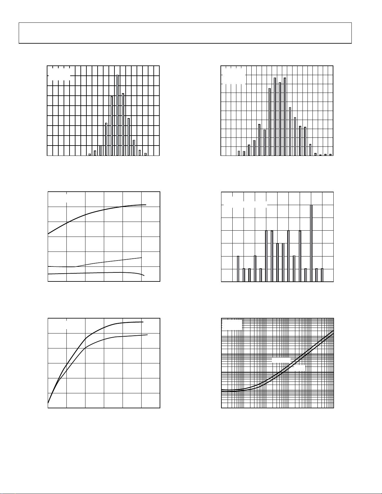
Figure 5. Input Offset Voltage Distribution
02735-003
100
VS = 5V
90
V
= 2.5V
CM
T
= 25°C
A
80
70
60
50
40
30
NUMBER OF AMPLIF IERS
20
10
0
–2.5 –1.5 –0.5 0.5 1.5 2.5
INPUT OFFSET VOLTAGE (µV)
Figure 8. Input Offset Voltage Distribution
02735-006
60
VS = 5V
50
40
30
20
INPUT BIAS CURRENT (pA)
10
0
012345
INPUT COMMON-MODE VOLTAGE (V)
+85°C
+25°C
–40°C
6
Figure 6. AD8628 Input Bias Current vs. Input Common-Mode Voltage
1500
VS = 5V
1000
500
0
–500
INPUT BIAS CURRENT (pA)
–1000
150°C
125°C
7
VS = 5V
T
= –40°C TO +125° C
6
A
5
4
3
2
NUMBER OF AMPLIF IERS
1
0
02735-004
0
2
4
TCVOS (nV/°C)
68
10
02735-007
Figure 9. Input Offset Voltage Drift
1k
VS = 5V
T
= 25°C
A
100
10
1
OUTPUT VOLTAGE (mV)
0.1
SOURCE
SINK
–1500
012345
INPUT COMMON-MODE VOLTAGE (V)
6
Figure 7. AD8628 Input Bias Current vs. Input Common-Mode Voltage
02735-005
Rev. G | Page 6 of 20
0.01
0.0001 0.001 0.10.01 1 10
LOAD CURRENT (mA)
Figure 10. Output Voltage to Supply Rail vs. Load Current
02735-008

AD8628/AD8629/AD8630
1k
VS = 2.7V
100
10
1
OUTPUT VOLTAGE (mV)
0.1
0.01
0.0001 0.001 0.10.01 1 10
SOURCE
SINK
LOAD CURRENT (mA)
Figure 11. Output Voltage to Supply Rail vs. Load Current
1500
VS = 5V
= 2.5V
V
CM
= –40°C TO + 150°C
T
A
1150
900
450
INPUT BIAS CURRENT (pA)
100
0
–50 0 25–25 50 75 100 125 150 175
TEMPERATURE (°C)
Figure 12. AD8628 Input Bias Current vs. Temperature
02735-009
02735-010
1000
TA = 25°C
800
600
400
SUPPLY CURRENT (µA)
200
0
012 4536
SUPPLY VOLTAGE (V)
02735-012
Figure 14. Supply Current vs. Supply Voltage
60
40
20
0
OPEN-LOOP GAIN (dB)
–20
10k 100k 1M 10M
GAIN
PHASE
FREQUENCY (Hz)
VS = 2.7V
C
= 20pF
L
R
= ∞
L
Ф
= 45°
M
0
45
90
135
180
225
PHASE SHIFT (Degrees)
02735-013
Figure 15. Open-Loop Gain and Phase vs. Frequency
1250
TA = 25°C
1000
750
500
SUPPLY CURRENT (µA)
250
0
–50 0 50 150100 200
TEMPERATURE (°
5V
2.7V
C
)
Figure 13. Supply Current vs. Temperature
02735-011
Rev. G | Page 7 of 20
70
60
50
40
30
20
10
0
OPEN-LOOP GAIN (dB)
–10
–20
–30
10k 100k 1M 10M
GAIN
PHASE
FREQUENCY (Hz)
Figure 16. Open-Loop Gain and Phase vs. Frequency
VS = 5V
C
= 20pF
L
R
= ∞
L
Φ
= 52.1°
M
0
45
90
135
180
225
PHASE SHIF T (Degrees)
02735-014

AD8628/AD8629/AD8630
70
60
50
AV = 100
40
30
AV = 10
20
10
AV = 1
0
CLOSED-LOOP GAIN (dB)
–10
–20
–30
1k 10k 100k 1M 10M
FREQUENCY ( Hz)
Figure 17. Closed-Loop Gain vs. Frequency
VS = 2.7V
C
= 20pF
L
R
= 2kΩ
L
02735-015
300
VS = 5V
270
240
210
180
150
120
90
OUTPUT IMPEDANCE (Ω)
60
30
0
100 1k 10k 100k 1M 10M 100M
AV = 100
AV = 10
AV = 1
FREQUENCY ( Hz)
Figure 20. Output Impedance vs. Frequency
02735-018
70
60
50
40
30
20
10
CLOSED-LOOP GAIN (dB)
–10
–20
–30
= 100
A
V
AV = 10
AV = 1
0
1k 10k 100k 1M 10M
FREQUENCY ( Hz)
Figure 18. Closed-Loop Gain vs. Frequency
300
VS = 2.7V
270
240
210
180
150
120
90
OUTPUT IMPEDANCE (Ω)
60
30
0
100 1k 10k 100k 1M 10M 100M
AV = 100
= 10
A
V
FREQUENCY (Hz)
AV = 1
Figure 19. Output Impedance vs. Frequency
VS = 5V
C
= 20pF
L
R
= 2kΩ
L
VS = ±1.35V
C
= 300pF
L
R
= ∞
0V
VOLTAGE (500mV/DIV)
02735-016
L
A
V
= 1
TIME (4µs/DIV)
02735-019
Figure 21. Large Signal Transient Response
VS = ±2.5V
C
= 300pF
L
R
= ∞
0V
VOLTAGE (1V/DIV)
02735-017
L
A
V
= 1
TIME (5µs/DIV)
02735-020
Figure 22. Large Signal Transient Response
Rev. G | Page 8 of 20

AD8628/AD8629/AD8630
T
T
80
VS = ±2.5V
R
= 2kΩ
L
70
T
= 25°C
A
60
50
40
30
OVERSHOOT (%)
20
OS–
OS+
10
0
110100
CAPACITIVE LOAD ( pF)
Figure 26. Small Signal Overshoot vs. Load Capacitance
1k
02735-024
AGE (50mV/DI V)
VOL
VS = ±1.35V
C
= 50pF
L
R
= ∞
L
A
= 1
V
0V
TIME (4µs/DIV)
Figure 23. Small Signal Transient Response
02735-021
VS = ±2.5V
C
= 50pF
L
R
= ∞
L
A
= 1
V
0V
AGE (50mV/DIV)
VOL
TIME (4µs/DIV)
Figure 24. Small Signal Transient Response
100
= ±1.35V
V
S
R
= 2kΩ
90
L
T
= 25°C
A
80
70
60
50
40
OVERSHOOT (%)
30
OS–
20
10
0
110100
CAPACITIVE LOAD ( pF)
Figure 25. Small Signal Overshoot vs. Load Capacitance
OS+
02735-022
1k
02735-023
VS = ±2.5V
A
= –50
V
IN
V
R
= 10kΩ
L
C
= 0pF
L
CH1 = 50mV/DIV
CH2 = 1V/DIV
0V
VOLTAGE (V)
0V
V
OUT
TIME (2µs/DIV)
02735-025
Figure 27. Positive Overvoltage Recovery
0V
VS = ±2.5V
A
= –50
V
R
= 10kΩ
V
IN
V
OUT
VOLTAGE (V)
L
C
= 0pF
L
CH1 = 50mV/DIV
CH2 = 1V/DIV
0V
TIME (10µ s/DIV)
02735-026
Figure 28. Negative Overvoltage Recovery
Rev. G | Page 9 of 20

AD8628/AD8629/AD8630
VS = ±2.5V
V
= 1kHz @ ±3V p-p
IN
C
= 0pF
L
R
= 10kΩ
L
A
= 1
V
0V
VOLTAGE (1V/DIV)
TIME (200µs/DIV)
02735-027
Figure 29. No Phase Reversal
140
VS = ±1.35V
120
100
80
60
40
PSRR (dB)
20
0
–20
–40
–60
100 1k 10k 100k 1M 10M
FREQUENCY (Hz)
+PSRR
–PSRR
Figure 32. PSRR vs. Frequency
02735-030
140
VS = 2.7V
120
100
80
60
40
CMRR (dB)
20
0
–20
–40
–60
100 1k 10k 100k 1M 10M
FREQUENCY (Hz)
Figure 30. CMRR vs. Frequency
140
VS = 5V
120
100
80
60
40
CMRR (dB)
20
0
–20
–40
–60
100 1k 10k 100k 1M 10M
FREQUENCY (Hz)
Figure 31. CMRR vs. Frequency
140
VS = ±2.5V
120
100
80
60
40
PSRR (dB)
20
0
–20
–40
–60
02735-028
100 1k 10k 100k 1M 10M
–PSRR
FREQUENCY (Hz)
+PSRR
02735-031
Figure 33. PSRR vs. Frequency
3.0
2.5
2.0
1.5
1.0
OUTPUT SWING (V p-p)
0.5
0
02735-029
100 1k 10k 100k 1M
FREQUENCY ( Hz)
VS = 2.7V
R
= 10kΩ
L
T
= 25°C
A
A
= 1
V
02735-032
Figure 34. Maximum Output Swing vs. Frequency
Rev. G | Page 10 of 20

AD8628/AD8629/AD8630
5.5
5.0
4.5
4.0
3.5
3.0
2.5
2.0
OUTPUT SWING (V p-p)
1.5
1.0
0.5
0
100 1k 10k 100k 1M
FREQUENCY ( Hz)
Figure 35. Maximum Output Swing vs. Frequency
VS = 5V
R
= 10kΩ
L
T
= 25°C
A
A
= 1
V
02735-033
120
VS = 2.7V
NOISE AT 1kHz = 21.3nV
105
90
75
60
45
30
VOLTAGE NOISE DENSITY (nV/ √Hz)
15
0
0 0. 5 1.0 1.5 2.0 2.5
FREQUENCY ( kHz)
Figure 38. Voltage Noise Density at 2.7 V from 0 Hz to 2.5 kHz
02735-036
0.60
VS = 2.7V
0.45
0.30
0.15
0
VOLTAGE (µV)
–0.15
–0.30
–0.45
–0.60
01 2345 67 8910
TIME (µs)
Figure 36. 0.1 Hz to 10 Hz Noise
0.60
VS = 5V
0.45
0.30
0.15
0
120
VS = 2.7V
NOISE AT 10kHz = 42.4nV
105
90
75
60
45
30
VOLTAGE NOISE DENSITY (nV/ √Hz)
15
0
02735-034
0 5 10 15 20 25
FREQUENCY (kHz)
02735-037
Figure 39. Voltage Noise Density at 2.7 V from 0 Hz to 25 kHz
120
VS = 5V
NOISE AT 1kHz = 22.1nV
105
90
75
60
VOLTAGE (µV)
–0.15
–0.30
–0.45
–0.60
01 2345 67 8910
TIME (µs)
Figure 37. 0.1 Hz to 10 Hz Noise
02735-035
Rev. G | Page 11 of 20
45
30
VOLTAGE NOISE DENSITY (nV/ √Hz)
15
0
0 0. 5 1.0 1.5 2.0 2.5
FREQUENCY ( kHz)
Figure 40. Voltage Noise Density at 5 V from 0 Hz to 2.5 kHz
02735-038

AD8628/AD8629/AD8630
120
VS = 5V
NOISE AT 10kHz = 36.4nV
105
90
150
100
VS = 2.7V
T
= –40°C TO +150° C
A
75
60
45
30
VOLTAGE NOISE DENSITY (nV/ √Hz)
15
0
0 5 10 15 20 25
FREQUENCY (kHz)
Figure 41. Voltage Noise Density at 5 V from 0 Hz to 25 kHz
120
VS = 5V
105
90
75
60
45
30
VOLTAGE NOISE DENSITY (nV/ √Hz)
15
0
05
FREQUENCY (kHz)
Figure 42. Voltage Noise Density at 5 V from 0 Hz to 10 kHz
OUTPUT SHO RT-CIRCUIT CURRENT (mA)
02735-039
OUTPUT SHO RT-CIRCUIT CURRENT (mA)
10
02735-040
–100
50
ISC–
0
ISC+
–50
–100
–50 25 50 750–25 100 125 150 175
TEMPERATURE (°C)
Figure 44. Output Short-Circuit Current vs. Temperature
150
VS = 5V
T
= –40°C TO +150°C
A
100
ISC–
50
0
–50
ISC+
–50 25 50 750–25 100 125 150 175
TEMPERATURE (°C)
Figure 45. Output Short-Circuit Current vs. Temperature
02735-042
02735-043
150
140
130
VS = 2.7V TO 5V
120
T
= –40°C TO +125° C
A
110
100
90
80
70
POWER SUPPLY REJECTION (dB)
60
50
–50 0 25–25 50 75 100 125
TEMPERATURE (°C)
Figure 43. Power Supply Rejection vs. Temperature
02735-041
Rev. G | Page 12 of 20
1k
VS = 5V
100
VOL– VEE@ 1kΩ
10
VCC– VOH@ 100kΩ
1
OUTPUT-TO-RAIL VOLTAGE (mV)
0.1
–50 25 50 750–25 100 125 150 175
VCC– VOH@ 1kΩ
VCC– VOH@ 10kΩ
VOL– VEE@ 10kΩ
VOL– VEE@ 100kΩ
TEMPERATURE (°C)
Figure 46. Output-to-Rail Voltage vs. Temperature
02735-044

AD8628/AD8629/AD8630
R
A
1k
VS = 2.7V
100
10
1
OUTPUT-TO-RAIL VOLTAGE (mV)
0.1
–50 25 50 750–25 100 125 150 175
VCC– VOH@ 1kΩ
VCC– VOH@ 10kΩ
VCC– VOH@ 100kΩ
TEMPERATURE (°C)
VOL– VEE@ 1kΩ
VOL– VEE@ 10kΩ
VOL– VEE@ 100kΩ
02735-045
Figure 47. Output-to-Rail Voltage vs. Temperature
140
120
100
TION (dB)
80
60
40
CHANNEL SEPA
20
V
IN
28mV p-p
0
1k 10k 100k 1M 10M
+2.5V
V+
+
AB
–
V–
–2.5V
FREQUENCY (Hz)
R1
10kΩ
V–
V
OUT
V+
VS = ±2.5V
R2
100Ω
Figure 48. AD8629/AD8630 Channel Separation vs. Frequency
02735-062
Rev. G | Page 13 of 20

AD8628/AD8629/AD8630
FUNCTIONAL DESCRIPTION
The AD8628/AD8629/AD8630 are single-supply, ultrahigh
precision rail-to-rail input and output operational amplifiers.
The typical offset voltage of less than 1 µV allows these amplifiers
to be easily configured for high gains without risk of excessive
output voltage errors. The extremely small temperature drift
of 2 nV/°C ensures a minimum offset voltage error over their
entire temperature range of −40°C to +125°C, making these
amplifiers ideal for a variety of sensitive measurement applications in harsh operating environments.
The AD8628/AD8629/AD8630 achieve a high degree of precision
through a patented combination of auto-zeroing and chopping.
This unique topology allows the AD8628/AD8629/AD8630 to
maintain their low offset voltage over a wide temperature range
and over their operating lifetime. The AD8628/AD8629/AD8630
also optimize the noise and bandwidth over previous generations
of auto-zero amplifiers, offering the lowest voltage noise of any
auto-zero amplifier by more than 50%.
Previous designs used either auto-zeroing or chopping to add
precision to the specifications of an amplifier. Auto-zeroing
results in low noise energy at the auto-zeroing frequency, at the
expense of higher low frequency noise due to aliasing of wideband
noise into the auto-zeroed frequency band. Chopping results in
lower low frequency noise at the expense of larger noise energy
at the chopping frequency. The AD8628/AD8629/AD8630
family uses both auto-zeroing and chopping in a patented pingpong arrangement to obtain lower low frequency noise together
with lower energy at the chopping and auto-zeroing frequencies,
maximizing the signal-to-noise ratio for the majority of
applications without the need for additional filtering. The
relatively high clock frequency of 15 kHz simplifies filter
requirements for a wide, useful noise-free bandwidth.
The AD8628 is among the few auto-zero amplifiers offered in
the 5-lead TSOT package. This provides a significant improvement
over the ac parameters of the previous auto-zero amplifiers. The
AD8628/AD8629/AD8630 have low noise over a relatively wide
bandwidth (0 Hz to 10 kHz) and can be used where the highest
dc precision is required. In systems with signal bandwidths of
from 5 kHz to 10 kHz, the AD8628/AD8629/AD8630 provide
true 16-bit accuracy, making them the best choice for very high
resolution systems.
1/f NOISE
1/f noise, also known as pink noise, is a major contributor to
errors in dc-coupled measurements. This 1/f noise error term
can be in the range of several µV or more, and, when amplified
with the closed-loop gain of the circuit, can show up as a large
output offset. For example, when an amplifier with a 5 µV p-p
1/f noise is configured for a gain of 1000, its output has 5 mV of
error due to the 1/f noise. However, the AD8628/AD8629/AD8630
eliminate 1/f noise internally, thereby greatly reducing output errors.
The internal elimination of 1/f noise is accomplished as follows.
1/f noise appears as a slowly varying offset to the AD8628/AD8629/
AD8630 inputs. Auto-zeroing corrects any dc or low frequency
offset. Therefore, the 1/f noise component is essentially removed,
leaving the AD8628/AD8629/AD8630 free of 1/f noise.
One advantage that the AD8628/AD8629/AD8630 bring to
system applications over competitive auto-zero amplifiers is their
very low noise. The comparison shown in Figure 49 indicates
an input-referred noise density of 19.4 nV/√Hz at 1 kHz for
the AD8628, which is much better than the Competitor A
and Competitor B. The noise is flat from dc to 1.5 kHz, slowly
increasing up to 20 kHz. The lower noise at low frequency is
desirable where auto-zero amplifiers are widely used.
120
COMPETITOR A
105
(89.7nV/ √Hz)
90
75
60
COMPETITOR B
45
(31.1nV/ √Hz)
30
VOLTAGE NOISE DENSI TY (nV/ √Hz)
15
AD8628
(19.4nV/ √Hz)
0
042861012
Figure 49. Noise Spectral Density of AD8628 vs. Competition
MK AT 1kHz FOR ALL 3 GRAPHS
FREQUENCY (kHz)
02735-046
Rev. G | Page 14 of 20

AD8628/AD8629/AD8630
PEAK-TO-PEAK NOISE
Because of the ping-pong action between auto-zeroing and
chopping, the peak-to-peak noise of the AD8628/AD8629/
AD8630 is much lower than the competition. Figure 50 and
Figure 51 show this comparison.
en p-p = 0.5µV
BW = 0.1Hz TO 10Hz
VOLTAGE (0.5µV/DIV)
TIME (1s/ DIV)
Figure 50. AD8628 Peak-to-Peak Noise
en p-p = 2.3µV
BW = 0.1Hz TO 10Hz
VOLTAGE (0.5µV/DIV)
50
45
40
35
30
25
NOISE (dB)
20
15
10
5
0
0 30 60 10090807050402010
FREQUENCY ( kHz)
02735-050
Figure 53. Simulation Transfer Function of the Test Circuit in Figure 52
50
45
40
02735-047
35
30
25
NOISE (dB)
20
15
10
5
0
0 30 60 10090807050402010
FREQUENCY ( kHz)
02735-051
Figure 54. Actual Transfer Function of the Test Circuit in Figure 52
The measured noise spectrum of the test circuit charted in
Figure 54 shows that noise between 5 kHz and 45 kHz is
successfully rolled off by the first-order filter.
TIME (1s/ DIV)
02735-048
Figure 51. Competitor A Peak-to-Peak Noise
NOISE BEHAVIOR WITH FIRST-ORDER, LOW-PASS FILTER
The AD8628 was simulated as a low-pass filter (see Figure 53)
and then configured as shown in Figure 52. The behavior of the
AD8628 matches the simulated data. It was verified that noise is
rolled off by first-order filtering. Figure 53 and Figure 54 show
the difference between the simulated and actual transfer functions
of the circuit shown in Figure 52.
IN
100kΩ
1kΩ
Figure 52. First-Order Low-Pass Filter Test Circuit,
×101 Gain and 3 kHz Corner Frequency
470pF
OUT
02735-049
Rev. G | Page 15 of 20
TOTAL INTEGRATED INPUT-REFERRED NOISE FOR FIRST-ORDER FILTER
For a first-order filter, the total integrated noise from the
AD8628 is lower than the noise of Competitor A.
10
COMPETITOR A
AD8551
1
RMS NOISE (µ V)
0.1
10 100 10k1k
3dB FILT ER BANDWIDTH (Hz)
Figure 55. RMS Noise vs. 3 dB Filter Bandwidth in Hz
AD8628
02735-052

AD8628/AD8629/AD8630
INPUT OVERVOLTAGE PROTECTION
Although the AD8628/AD8629/AD8630 are rail-to-rail input
amplifiers, care should be taken to ensure that the potential
difference between the inputs does not exceed the supply voltage.
Under normal negative feedback operating conditions, the
amplifier corrects its output to ensure that the two inputs are at
the same voltage. However, if either input exceeds either supply
rail by more than 0.3 V, large currents begin to flow through the
ESD protection diodes in the amplifier.
These diodes are connected between the inputs and each supply
rail to protect the input transistors against an electrostatic discharge
event, and they are normally reverse-biased. However, if the input
voltage exceeds the supply voltage, these ESD diodes can become
forward-biased. Without current limiting, excessive amounts
of current could flow through these diodes, causing permanent
damage to the device. If inputs are subject to overvoltage,
appropriate series resistors should be inserted to limit the diode
current to less than 5 mA maximum.
OUTPUT PHASE REVERSAL
Output phase reversal occurs in some amplifiers when the input
common-mode voltage range is exceeded. As common-mode
voltage is moved outside the common-mode range, the outputs of
these amplifiers can suddenly jump in the opposite direction to
the supply rail. This is the result of the differential input pair
shutting down, causing a radical shifting of internal voltages
that results in the erratic output behavior.
The AD8628/AD8629/AD8630 amplifiers have been carefully
designed to prevent any output phase reversal, provided that
both inputs are maintained within the supply voltages. If one or
both inputs could exceed either supply voltage, a resistor should
be placed in series with the input to limit the current to less than
5 mA. This ensures that the output does not reverse its phase.
OVERLOAD RECOVERY TIME
Many auto-zero amplifiers are plagued by a long overload recovery
time, often in ms, due to the complicated settling behavior of
the internal nulling loops after saturation of the outputs. The
AD8628/AD8629/AD8630 have been designed so that internal
settling occurs within two clock cycles after output saturation
occurs. This results in a much shorter recovery time, less
than 10 µs, when compared to other auto-zero amplifiers. The
wide bandwidth of the AD8628/AD8629/AD8630 enhances
performance when the parts are used to drive loads that inject
transients into the outputs. This is a common situation when an
amplifier is used to drive the input of switched capacitor ADCs.
V
IN
0V
VOLTAGE (V)
0V
V
OUT
TIME (500µ s/DIV)
Figure 56. Positive Input Overload Recovery for the AD8628
V
IN
0V
VOLTAGE (V)
0V
V
OUT
TIME (500µ s/DIV)
Figure 57. Positive Input Overload Recovery for Competitor A
V
IN
0V
0V
VOLTAGE (V)
V
OUT
TIME (500µ s/DIV)
Figure 58. Positive Input Overload Recovery for Competitor B
CH1 = 50mV/DIV
CH2 = 1V/DIV
A
= –50
V
CH1 = 50mV/DIV
CH2 = 1V/DIV
A
= –50
V
CH1 = 50mV/DIV
CH2 = 1V/DIV
A
= –50
V
02735-053
02735-054
02735-055
Rev. G | Page 16 of 20

AD8628/AD8629/AD8630
Ω
The results shown in Figure 56 to Figure 61 are summarized in
0V
V
IN
VOLTAGE (V)
V
OUT
CH1 = 50mV/DIV
CH2 = 1V/DIV
A
= –50
V
Table 5.
Table 5. Overload Recovery Time
Model
Positive Overload
Recovery (μs)
Negative Overload
Recovery (μs)
AD8628 6 9
Competitor A 650 25,000
Competitor B 40,000 35,000
0V
TIME (500µ s/DIV)
Figure 59. Negative Input Overload Recovery for the AD8628
0V
V
IN
V
OUT
VOLTAGE (V)
0V
TIME (500µ s/DIV)
Figure 60. Negative Input Overload Recovery for Competitor A
0V
V
IN
V
OUT
CH1 = 50mV/DIV
CH2 = 1V/DIV
A
= –50
V
CH1 = 50mV/DIV
CH2 = 1V/DIV
A
= –50
V
INFRARED SENSORS
Infrared (IR) sensors, particularly thermopiles, are increasingly
02735-056
02735-057
being used in temperature measurement for applications as wide
ranging as automotive climate control, human ear thermometers,
home insulation analysis, and automotive repair diagnostics.
The relatively small output signal of the sensor demands high
gain with very low offset voltage and drift to avoid dc errors.
If interstage ac coupling is used, as in Figure 62, low offset and
drift prevent the output of the input amplifier from drifting close to
saturation. The low input bias currents generate minimal errors
from the output impedance of the sensor. As with pressure sensors,
the very low amplifier drift with time and temperature eliminate
additional errors once the temperature measurement is calibrated.
The low 1/f noise improves SNR for dc measurements taken
over periods often exceeding one-fifth of a second.
Figure 62 shows a circuit that can amplify ac signals from 100 µV to
300 µV up to the 1 V to 3 V levels, with a gain of 10,000 for
accurate analog-to-digital conversion.
100k
5V
1/2 AD8629
02735-059
≈ 1.6Hz
f
C
10kΩ
10µF
10kΩ
TO BIAS
VOLTAGE
100Ω
100µV TO 300µV
IR
DETECT OR
100kΩ
5V
1/2 AD8629
Figure 62. AD8629 Used as Preamplifier for Thermopile
VOLTAGE (V)
0V
TIME (500µ s/DIV)
02735-058
Figure 61. Negative Input Overload Recovery for Competitor B
Rev. G | Page 17 of 20

AD8628/AD8629/AD8630
V
V
PRECISION CURRENT SHUNT SENSOR OUTPUT AMPLIFIER FOR HIGH PRECISION DACS
A precision current shunt sensor benefits from the unique
attributes of auto-zero amplifiers when used in a differencing
configuration, as shown in Figure 63. Current shunt sensors are
used in precision current sources for feedback control systems.
They are also used in a variety of other applications, including
battery fuel gauging, laser diode power measurement and control,
torque feedback controls in electric power steering, and precision
power metering.
SUPPLY
e = 1000 RSI
100mV/m A
S
0.1Ω
I
100Ω100kΩ
C
5V
R
L
R
AD8628
100Ω100kΩ
C
Figure 63. Low-Side Current Sensing
02735-060
In such applications, it is desirable to use a shunt with very low
resistance to minimize the series voltage drop; this minimizes
wasted power and allows the measurement of high currents
while saving power. A typical shunt might be 0.1 Ω. At measured
current values of 1 A, the output signal of the shunt is hundreds
of millivolts, or even volts, and amplifier error sources are not
critical. However, at low measured current values in the 1 mA
range, the 100 µV output voltage of the shunt demands a very
low offset voltage and drift to maintain absolute accuracy. Low
input bias currents are also needed, so that injected bias current
does not become a significant percentage of the measured current.
High open-loop gain, CMRR, and PSRR help to maintain the
overall circuit accuracy. As long as the rate of change of the
current is not too fast, an auto-zero amplifier can be used with
excellent results.
The AD8628/AD8629/AD8360 are used as output amplifiers for
a 16-bit high precision DAC in a unipolar configuration. In this
case, the selected op amp needs to have a very low offset voltage
(the DAC LSB is 38 µV when operated with a 2.5 V reference)
to eliminate the need for output offset trims. The input bias
current (typically a few tens of picoamperes) must also be very
low because it generates an additional zero code error when
multiplied by the DAC output impedance (approximately 6 kΩ).
Rail-to-rail input and output provide full-scale output with very
little error. The output impedance of the DAC is constant and
code independent, but the high input impedance of the AD8628/
AD8629/AD8630 minimizes gain errors. The wide bandwidth
of the amplifiers also serves well in this case. The amplifiers,
with settling time of 1 µs, add another time constant to the
system, increasing the settling time of the output. The settling
time of the AD5541 is 1 µs. The combined settling time is
approximately 1.4 µs, as can be derived from the following
equation:
22
()( )( )
AD8628
tDACtTOTALt +=
SSS
2.5
SERIAL
INTERFACE
*AD5542 ONLY
5
0.1µF
REF(REFF*) REFS*
V
DD
CS
DIN
AD5541/AD5542
SCLK
LDAC*
DGND
Figure 64. AD8628 Used as an Output Amplifier
0.1µF
10µF
AGND
V
AD8628
OUT
UNIPOLAR
OUTPUT
02735-061
Rev. G | Page 18 of 20

AD8628/AD8629/AD8630
OUTLINE DIMENSIONS
2.90 BSC
5.00 (0.1968)
4.80 (0.1890)
54
0.50
0.30
2.80 BSC
0.95 BSC
*
1.00 MAX
SEATING
PLANE
0.20
0.08
8°
4°
0°
1.60 BSC
*
0.90
0.87
0.84
0.10 MAX
123
PIN 1
1.90
BSC
*
COMPLIANT TO JEDEC STANDARDS MO-193-AB WITH
THE EXCEPTION OF PACKAGE HEIGHT AND THICKNESS.
Figure 65. 5-Lead Thin Small Outline Transistor Package [TSOT]
(UJ-5)
Dimensions shown in millimeters
2.90 BSC
1.60 BSC
1.30
1.15
0.90
0.15 MAX
5
123
PIN 1
COMPLIANT TO JEDEC STANDARDS MO-178-A A
1.90
BSC
0.50
0.30
4
0.95 BSC
2.80 BSC
1.45 MAX
SEATING
PLANE
0.22
0.08
10°
5°
0°
Figure 66. 5-Lead Small Outline Transistor Package [SOT-23]
(RJ-5)
Dimensions shown in millimeters
0.60
0.45
0.30
0.60
0.45
0.30
4.00 (0.1574)
3.80 (0.1497)
0.25 (0.0098)
0.10 (0.0040)
COPLANARI TY
0.10
CONTROL LING DIMENSI ONS ARE IN MILL IMET ERS; INCH DI MENSIO NS
(IN PARENTHESES ) ARE ROUNDED- OFF MI LLI METER EQ UIVALENTS FOR
REFERENCE ONLY AND ARE NOT APPROPRI ATE FOR USE I N DESIG N.
85
1
1.27 (0.0500)
SEATING
PLANE
COMPLI ANT TO JEDE C STANDARDS MS-012-A A
BSC
6.20 (0.2441)
5.80 (0.2284)
4
1.75 (0.0688)
1.35 (0.0532)
0.51 (0.0201)
0.31 (0.0122)
8°
0°
0.25 (0.0098)
0.17 (0.0067)
0.50 (0.0196)
0.25 (0.0099)
1.27 (0.0500)
0.40 (0.0157)
45°
012407-A
Figure 67. 8-Lead Standard Small Outline Package [SOIC_N]
Narrow Body
(R-8)
Dimensions shown in millimeters and (inches)
3.20
3.00
2.80
8
5
4
SEATING
PLANE
5.15
4.90
4.65
1.10 MAX
0.23
0.08
8°
0°
0.80
0.60
0.40
3.20
3.00
1
2.80
PIN 1
0.65 BSC
0.95
0.85
0.75
0.15
0.38
0.00
0.22
COPLANARITY
0.10
COMPLIANT TO JEDEC STANDARDS MO-187-AA
Figure 68. 8-Lead Mini Small Outline Package [MSOP]
(RM-8)
Dimensions shown in millimeters
Rev. G | Page 19 of 20

AD8628/AD8629/AD8630
5.10
8.75 (0.3445)
8.55 (0.3366)
BSC
8
7
6.20 (0.2441)
5.80 (0.2283)
1.75 (0.0689)
1.35 (0.0531)
SEATING
PLANE
8°
0°
0.25 (0.0098)
0.17 (0.0067)
0.50 (0.0197)
0.25 (0.0098)
1.27 (0.0500)
0.40 (0.0157)
4.50
4.40
45°
4.30
PIN 1
1.05
1.00
0.80
060606-A
Figure 70. 14-Lead Thin Shrink Small Outline Package [TSSOP]
4.00 (0.1575)
3.80 (0.1496)
0.25 (0.0098)
0.10 (0.0039)
COPLANARIT Y
0.10
14
1
1.27 (0.0500)
0.51 (0.0201)
0.31 (0.0122)
CONTROLL ING DIMENS IONS ARE IN MILLIM ETERS; INCH DI MENSIONS
(IN PARENTHESES) ARE ROUNDED- OFF MIL LIMET ER EQUIVALENTS FOR
REFERENCE ON LY AND ARE NOT APPROPRI ATE FOR USE IN DES IGN.
COMPLIANT TO JEDEC STANDARDS MS-012-AB
Figure 69. 14-Lead Standard Small Outline Package [SOIC_N]
Narrow Body (R-14)
Dimensions shown in millimeters and (inches)
ORDERING GUIDE
Model Temperature Range Package Description Package Option Branding
AD8628AUJ-R2 −40°C to +125°C 5-Lead TSOT UJ-5 AYB
AD8628AUJ-REEL −40°C to +125°C 5-Lead TSOT UJ-5 AYB
AD8628AUJ-REEL7 −40°C to +125°C 5-Lead TSOT UJ-5 AYB
AD8628AUJZ-R2
AD8628AUJZ-REEL
AD8628AUJZ-REEL7
AD8628AR −40°C to +125°C 8-Lead SOIC_N R-8
AD8628AR-REEL −40°C to +125°C 8-Lead SOIC_N R-8
AD8628AR-REEL7 −40°C to +125°C 8-Lead SOIC_N R-8
AD8628ARZ
AD8628ARZ-REEL
AD8628ARZ-REEL7
AD8628ART-R2 −40°C to +125°C 5-Lead SOT-23 RJ-5 AYA
AD8628ART-REEL7 −40°C to +125°C 5-Lead SOT-23 RJ-5 AYA
AD8628ARTZ-R2
AD8628ARTZ-REEL7
AD8629ARZ
AD8629ARZ-REEL
AD8629ARZ-REEL7
AD8629ARMZ-R2
AD8629ARMZ-REEL
AD8630ARUZ
AD8630ARUZ-REEL
AD8630ARZ
AD8630ARZ-REEL
AD8630ARZ-REEL7
1
Z = RoHS Compliant Part.
1
−40°C to +125°C 5-Lead TSOT UJ-5 A0L
1
−40°C to +125°C 5-Lead TSOT UJ-5 A0L
1
−40°C to +125°C 5-Lead TSOT UJ-5 A0L
1
−40°C to +125°C 8-Lead SOIC_N R-8
1
−40°C to +125°C 8-Lead SOIC_N R-8
1
−40°C to +125°C 8-Lead SOIC_N R-8
1
−40°C to +125°C 5-Lead SOT-23 RJ-5 A0L
1
1
1
−40°C to +125°C 5-Lead SOT-23 RJ-5 A0L
−40°C to +125°C 8-Lead SOIC_N R-8
1
−40°C to +125°C 8-Lead SOIC_N R-8
1
−40°C to +125°C 8-Lead SOIC_N R-8
1
−40°C to +125°C 8-Lead MSOP RM-8 A06
1
−40°C to +125°C 8-Lead MSOP RM-8 A06
1
−40°C to +125°C 14-Lead TSSOP RU-14
1
−40°C to +125°C 14-Lead TSSOP RU-14
−40°C to +125°C 14-Lead SOIC_N R-14
1
−40°C to +125°C 14-Lead SOIC_N R-14
1
−40°C to +125°C 14-Lead SOIC_N R-14
5.00
4.90
14
0.15
0.05
0.65
BSC
0.30
0.19
8
6.40
BSC
71
1.20
MAX
SEATING
PLANE
0.20
0.09
COPLANARITY
0.10
COMPLIANT TO JEDEC STANDARDS MO-153-AB-1
(RU-14)
Dimensions shown in millimeters
8°
0°
0.75
0.60
0.45
©2002–2008 Analog Devices, Inc. All rights reserved. Trademarks and
registered trademarks are the property of their respective owners.
D02735-0-6/08(G)
Rev. G | Page 20 of 20
 Loading...