ANALOG DEVICES AD8627 Service Manual

Precision Low Power
www.BDTIC.com/ADI
FEATURES
SC70 package
Very low I
Single-supply operation: 5 V to 26 V
Dual-supply operation: ±2.5 V to ±13 V
Rail-to-rail output
Low supply current: 630 µA/amp typ
Low offset voltage: 500 µV max
Unity gain stable
No phase reversal
APPLICATIONS
Photodiode amplifiers
ATEs
Line-powered/battery-powered instrumentation
Industrial controls
Automotive sensors
Precision filters
Audio
GENERAL DESCRIPTION
The AD862x is a precision JFET input amplifier. It features
true single-supply operation, low power consumption, and
rail-to-rail output. The outputs remain stable with capacitive
loads of over 500 pF; the supply current is less than 630 µA/amp.
Applications for the AD862x include photodiode transimpedance
amplification, ATE reference level drivers, battery management,
both line powered and portable instrumentation, and remote
sensor signal conditioning, which includes automotive sensors.
: 1 pA max
B
Single-Supply JFET Amplifiers
AD8625/AD8626/AD8627
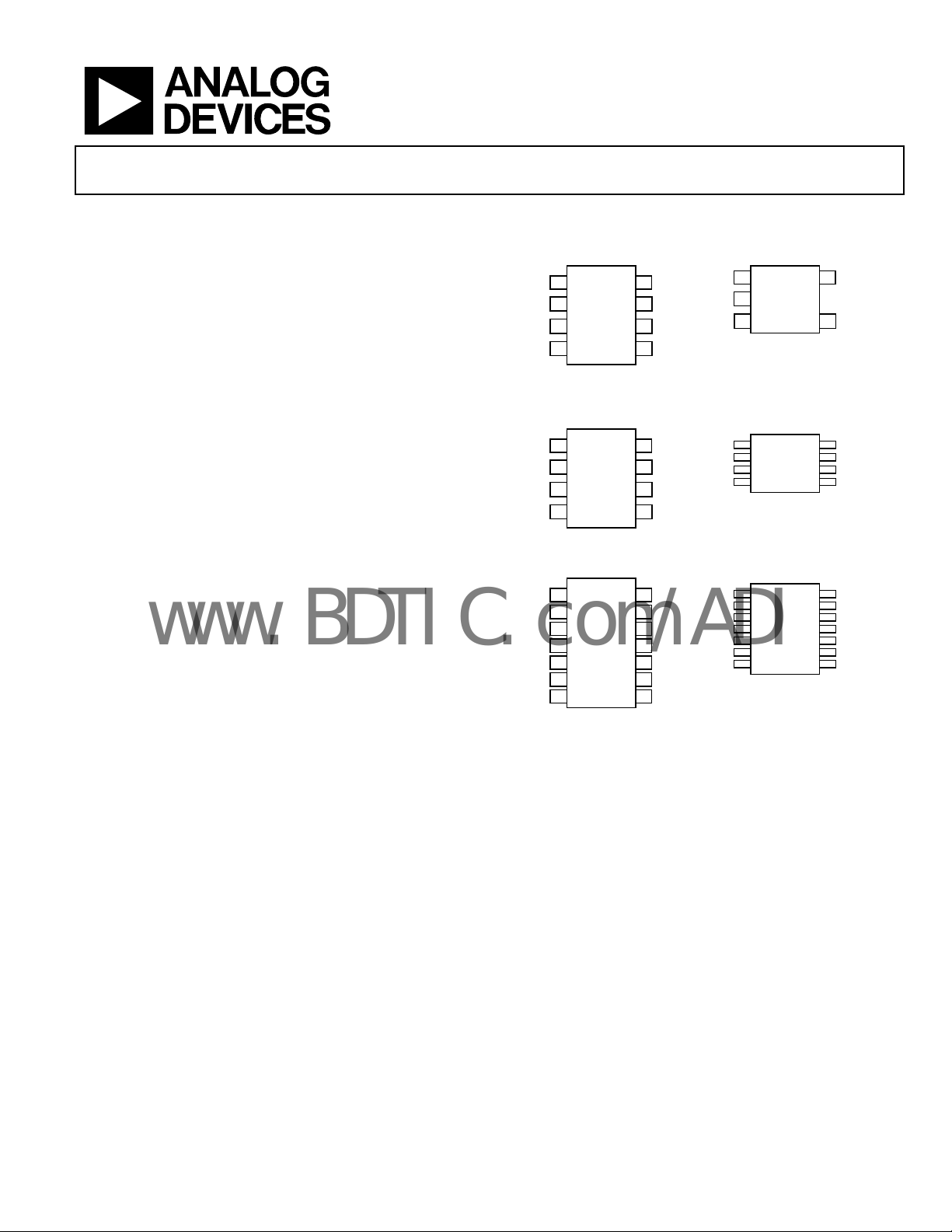
PIN CONFIGURATIONS
8-Lead SOIC
(R-8 Suffix)
NC
1
2
–IN V+
AD8627
3
+IN OUT
4
V– NC
NC = NO CONNECT
8-Lead SOIC
(R-8 Suffix)
OUT A
1
2
–IN A OUT B
+IN A –IN B
OUT A OUT D
–IN A –IN D
+IN A +IN D
+IN B +IN C
–IN B –IN C
OUT B OUT C
AD8626
3
4
V– +IN B
14-Lead SOIC
(R-Suffix)
114
213
312
AD8625
V+ V–
411
510
69
78
NC
8
7
6
5
V+
8
7
6
5
Figure 1.
5-Lead SC70
1
2
V–
+IN
3
8-Lead MSOP
1
4
14-Lead TSSOP
1
7
(KS Suffix)
AD8627
(RM-Suffix)
AD8626
(RU-Suffix)
AD8625
5OUT A
V+
–IN
4
8
V+OUT A
OUT B–IN A
–IN B+IN A
+IN BV–
5
14
OUT DOUT A
–IN D–IN A
+IN D+IN A
V–V+
+IN C+IN B
–IN C–IN B
OUT COUT B
8
03023-001
The AD862x’s ability to swing nearly rail-to-rail at the input
and rail-to-rail at the output enables it to be used to buffer
CMOS DACs, ASICs, and other wide output swing devices in
single-supply systems.
The 5 MHz bandwidth and low offset are ideal for precision
filters.
The AD862x is fully specified over the industrial temperature
range. (–40°C to +85°C). The AD8627 is available in both
5-lead SC70 and 8-lead SOIC surface-mount packages (SC70
packaged parts are available in tape and reel only). The AD8626
is available in MSOP and SOIC packages, while the AD8625 is
available in TSSOP and SOIC packages.
Rev. C
Information furnished by Analog Devices is believed to be accurate and reliable.
However, no responsibility is assumed by Analog Devices for its use, nor for any
infringements of patents or other rights of third parties that may result from its use.
Specifications subject to change without notice. No license is granted by implication
or otherwise under any patent or patent rights of Anal og Devices. Trademarks and
registered trademarks are the property of their respective owners.
One Technology Way, P.O. Box 9106, Norwood, MA 02062-9106, U.S.A.
Tel: 781.329.4700 www.analog.com
Fax: 781.326.8703 © 2004 Analog Devices, Inc. All rights reserved.

AD8625/AD8626/AD8627
www.BDTIC.com/ADI
TABLE OF CONTENTS
AD8625/AD8626/AD8627 Specifications..................................... 3
Electrical Characteristics............................................................. 3
Electrical Characteristics............................................................. 4
Absolute Maximum Ratings............................................................ 5
Typical Performance Characteristics............................................. 6
Applications..................................................................................... 13
REVISION HISTORY
11/04—Data Sheet Changed from Rev. B to Rev. C
Updated Figure Codes .......................................................Universal
hanges to Figure 17 and 18........................................................... 8
C
Changes to Figure 33 and Figure 37............................................. 11
Changes to Figure 38...................................................................... 12
Changes to Figure 39 and Figure 40............................................. 13
Changes to Figure 41 to Figure 44................................................ 14
1/04—Data Sheet Changed from Rev. A to Rev. B
Change to General Description...................................................... 1
C
hange to Figure 10 ......................................................................... 7
Change to Figure13 .......................................................................... 7
Change to Figure 37 ....................................................................... 11
Changes to Figure 38...................................................................... 12
Change to Output Amplifier for DACs section.......................... 15
Updated Outline Dimensions....................................................... 19
Minimizing Input Current........................................................ 15
Photodiode Preamplifier Application...................................... 15
Output Amplifier for DACs...................................................... 16
Eight-Pole Sallen Key Low-Pass Filter..................................... 17
Outline Dimensions .......................................................................18
Ordering Guide .......................................................................... 19
10/03—Data Sheet Changed from Rev. 0 to Rev. A
Addition of two new parts
Change to General Description
Changes to Pin Configurations
Change to Specifications table
Changes to Figure 31
Changes to Figure 32
Changes to Figure 38
Changes to Figure 46
Changes to Figure 47
Changes to Figure 49
Updated Outline Dimensions....................................................... 18
Changes to Ordering Guide
…………………………………Universal
………………………………………. 1
…………………....................................1
…………………………………………3
…………………………….................................... 10
…………………………….....................................11
…………………………….................................... 12
…………………………….................................... 16
…………………………….....................................16
…………………………….....................................17
…………………........................................ 19
Rev. C | Page 2 of 20

AD8625/AD8626/AD8627
www.BDTIC.com/ADI
AD8625/AD8626/AD8627 SPECIFICATIONS
ELECTRICAL CHARACTERISTICS
@VS = 5 V, VCM = 1.5 V, TA = 25°C, unless otherwise noted.
Table 1.
Parameter Symbol Conditions Min Typ Max Unit
INPUT CHARACTERISTICS
Offset Voltage VOS 0.05 0.5 mV
−40°C < TA < +85°C 1.2 mV
Input Bias Current I
–40°C < TA < +85°C 60 pA
Input Offset Current I
–40°C < TA < +85°C 25 pA
Input Voltage Range 0 3 V
Common-Mode Rejection Ratio CMRR VCM = 0 V to 2.5 V 66 87 dB
Large Signal Voltage Gain A
Offset Voltage Drift ∆VOS/∆T –40°C < TA < +85°C 2.5 µV/°C
OUTPUT CHARACTERISTICS
Output Voltage High V
I
Output Voltage Low V
I
Output Current I
POWER SUPPLY
Power-Supply Rejection Ratio PSRR VS = 5 V to 26 V 80 104 dB
Supply Current/Amplifier I
–40°C < TA < +85°C 800 µA
DYNAMIC PERFORMANCE
Slew Rate SR 5 V/µs
Gain Bandwidth Product GBP 5 MHz
Phase Margin Ø
NOISE PERFORMANCE
Voltage Noise en p-p 0.1 Hz to 10 Hz 1.9 µV p-p
Voltage Noise Density e
Current Noise Density i
Channel Separation C
B
OS
VO
OH
OL
OUT
SY
M
n
n
s
0.25 1 pA
0.5 pA
RL = 10 kΩ, VO = 0.5 V to 4.5 V 100 230 V/mV
4.92 V
= 2 mA, –40°C < TA < +85°C 4.90 V
L
0.075 V
= 2 mA, –40°C < TA < +85°C 0.08 V
L
±10 mA
630 785 µA
60 Degrees
f = 1 kHz 17.5 nV/√Hz
f = 1 kHz 0.4 fA/√Hz
f = 1 kHz 104 dB
Rev. C | Page 3 of 20

AD8625/AD8626/AD8627
www.BDTIC.com/ADI
ELECTRICAL CHARACTERISTICS
@VS = ±13 V; VCM = 0 V; TA = 25°C, unless otherwise noted.
Table 2.
Parameter Symbol Conditions Min Typ Max Unit
INPUT CHARACTERISTICS
Offset Voltage V
OS
–40°C < TA < +85°C 1.35 mV
Input Bias Current I
B
–40°C < TA < +85°C 60 pA
Input Offset Current I
OS
–40°C < TA < +85°C 25 pA
Input Voltage Range –13 +11 V
Common-Mode Rejection Ratio CMRR V
Large Signal Voltage Gain A
VO
Offset Voltage Drift ∆VOS/∆T –40°C < TA < +85°C 2.5 µV/°C
OUTPUT CHARACTERISTICS
Output Voltage High V
V
Output Voltage Low V
V
Output Current I
OH
OH
OL
OL
OUT
POWER SUPPLY
Power-Supply Rejection Ratio PSRR VS = ±2.5 V to ±13 V 80 104 dB
Supply Current/Amplifier I
SY
–40°C < TA < +85°C 900 µA
DYNAMIC PERFORMANCE
Slew Rate SR 5 V/µs
Gain Bandwidth Product GBP 5 MHz
Phase Margin Ø
M
NOISE PERFORMANCE
Voltage Noise en p-p 0.1 Hz to 10 Hz 2.5 µV p-p
Voltage Noise Density e
Current Noise Density i
Channel Separation C
n
n
s
0.35 0.75 mV
0.25 1 pA
0.5 pA
= –13 V to +10 V 76 105 dB
CM
RL = 10 kΩ, VO = –11 V to +11 V 150 310 V/mV
+12.92 V
IL = 2 mA, –40°C < TA < +85°C +12.91 V
–12.92 V
IL = 2 mA, –40°C < TA < +85°C –12.91 V
±15 mA
710 850 µA
60 Degrees
f = 1 kHz 16 nV/√Hz
f = 1 kHz 0.5 fA/√Hz
f = 1 kHz 105 dB
Rev. C | Page 4 of 20

AD8625/AD8626/AD8627
www.BDTIC.com/ADI
ABSOLUTE MAXIMUM RATINGS
Absolute maximum ratings apply at 25°C, unless otherwise
noted.
Table 3. Stress Ratings
Parameter Ratings
Supply Voltage 27 V
Input Voltage VS– to V
Differential Input Voltage ± Supply Voltage
Output Short-Circuit Duration Indefinite
Storage Temperature Range, R Package
Operating Temperature Range
Junction Temperature Range, R Package
Lead Temperature Range (Soldering, 60 sec) 300°C
Table 4.
Package Type θJA
5-Lead SC70 (KS) 376 126 °C/W
8-Lead MSOP (RM) 210 45 °C/W
8-Lead SOIC (R) 158 43 °C/W
14-Lead SOIC (R) 120 36 °C/W
14-Lead TSSOP (RU) 180 35 °C/W
1
θJA is specified for worst-case conditions when devices are soldered in circuit
boards for surface-mount packages.
1
θ
JC
S+
−65°C to +125°C
−40°C to +85°C
−65°C to +150°C
Unit
Stresses above those listed under Absolute Maximum Ratings
may cause permanent damage to the device. This is a stress
rating only; functional operation of the device at these or any
other conditions above those indicated in the operational
sections of this specification is not implied. Exposure to
absolute maximum rating conditions for extended periods may
affect device reliability.
ESD CAUTION
ESD (electrostatic discharge) sensitive device. Electrostatic charges as high as 4000 V readily accumulate on
the human body and test equipment and can discharge without detection. Although this product features
proprietary ESD protection circuitry, permanent damage may occur on devices subjected to high energy
electrostatic discharges. Therefore, proper ESD precautions are recommended to avoid performance
degradation or loss of functionality.
Rev. C | Page 5 of 20

AD8625/AD8626/AD8627
www.BDTIC.com/ADI
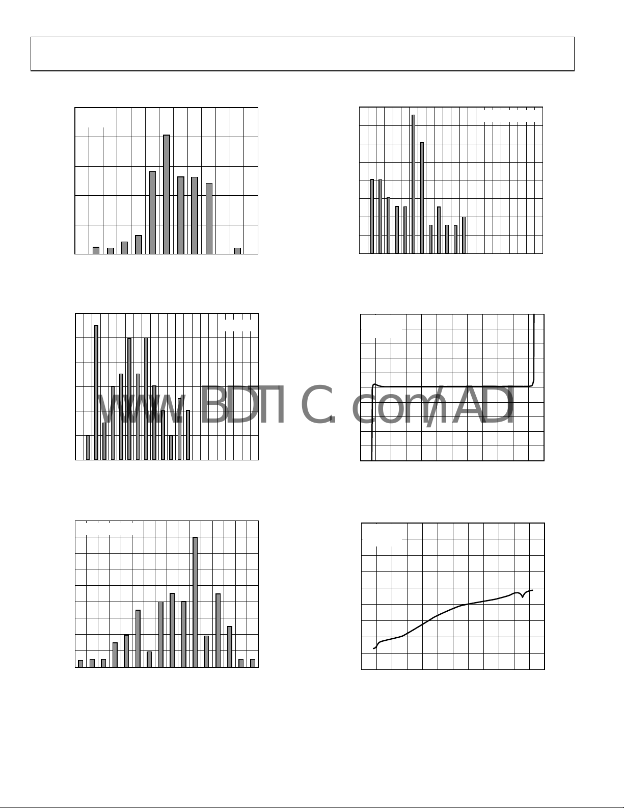
TYPICAL PERFORMANCE CHARACTERISTICS
25
VSY =±12V
= 25°C
T
A
20
16
14
12
VSY = +3.5V/–1.5V
15
10
NUMBER OF AMPLIFIERS
5
0
–600 –400
–200
VOLTAGE (µV)
0 200 400 600
Figure 2. Input Offset Voltage
12
10
8
6
4
NUMBER OF AMPLIFIERS
2
0
012345678910
OFFSET VO LTAGE (µV/°C)
Figure 3. Offset Voltage Drift
18
VSY = +3.5V/–1.5V
16
14
12
10
8
6
NUMBER OF AMPLIFIERS
4
2
0
–400 –300 –200 –100 0 100 200 300
VOLTAGE (µV)
Figure 4. Input Offset Voltage
VSY =±13V
03023-002
03023-003
03023-004
10
8
6
NUMBER OF AMPLIFIERS
4
2
0
012345678910
OFFSET VO LTAGE (µV/°C)
Figure 5. Offset Voltage Drift
50
VSY =±13V
T
= 25°C
40
A
30
20
10
0
–10
–20
INPUT BIAS CURRENT (pA)
–30
–40
–50
–15.0–12.5–10.0 –7.5 –5.0 –2.5 0 2.5 5.0 7.5 10.0 12.5 15.0
Figure 6. Input Bias Current vs. V
VCM (V)
CM
0
VSY =±13V
–0.1
= 25°C
T
A
–0.2
–0.3
–0.4
–0.5
–0.6
INPUT BIAS CURRENT (pA)
–0.7
–0.8
–0.9
–15.0–12.5–10.0 –7.5 –5.0 –2.5 0 2.5 5.0 7.5 10.0 12.5 15.0
Figure 7. Input Bias Current vs. V
VCM (V)
CM
03023-005
03023-006
03023-007
Rev. C | Page 6 of 20
 Loading...