

Low Power, Precision
AD8622/AD8624
OUT A
1
–IN A
2
+IN A
3
V–
4
V+
8
OUT B
7
–IN B
6
+IN B
5
AD8622
TOP VIEW
(Not to Scale)
07527-001
OUT A
1
–IN A
2
+IN A
3
V–
4
V+
8
OUT B
7
–IN B
6
+IN B
5
AD8622
TOP VIEW
(Not to S cale)
07527-002
07527-067
AD8624
1
2
3
4
5
6
7
14
13
12
11
10
9
8
TOP VIEW
(Not to S cale)
OUT A
OUT D
–IN D
+IN D
V–
+IN C
–IN C
OUT C
–IN A
+IN A
V+
+IN B
–IN B
OUT B
07527-068
NOTES
1. NC = NO CONNECT.
2. IT IS RECOMMENDED THAT THE EXPOSED
PAD BE CONNECTE D TO V–.
12
11
10
1
3
4
–IN D
+IN D
V–
9
+IN C
–IN A
V+
2
+IN A
+IN B
6OUT B
5–IN B
7OUT C
8
–IN C
16
NC
15
OUT A
14
OUT D
13
NC
TOP VIEW
(Not to Scale)
AD8624
FEATURES
Very low offset voltage
125 μV maximum
Supply current: 215 μA/amp typical
Input bias current: 200 pA maximum
Low input offset voltage drift: 1.2 μV/°C maximum
Very low voltage noise: 11 nV/√Hz
Operating temperature: −40°C to +125°C
Rail-to-rail output swing
Unity gain stable
±2.5 V to ±15 V operation
APPLICATIONS
Portable precision instrumentation
Laser diode control loops
Strain gage amplifiers
Medical instrumentation
Thermocouple amplifiers
Rail-to-Rail Output Op Amp
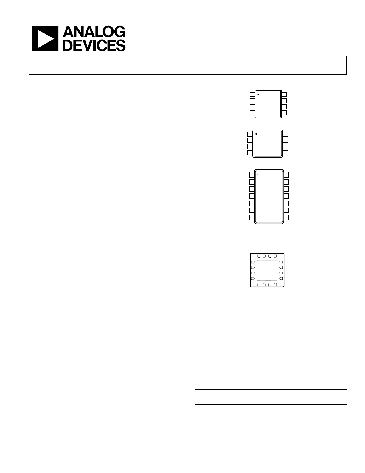
PIN CONFIGURATIONS
Figure 1. 8-Lead Narrow-Body SOIC
Figure 2. 8-Lead MSOP
GENERAL DESCRIPTION
The AD8622/AD8624 are dual and quad precision rail-to-rail
output operational amplifiers with low supply currents of only
350 µA/amplifier maximum over temperature and supply
voltages. The AD8622/AD8624 also has an input bias current
cancellation circuitry that provides a very low input bias current
over the full operating temperature.
With a typical offset voltage of only 10 µV, offset drift of 0.5 µV/°C,
and noise of only 0.2 μV p-p (0.1 Hz to 10 Hz), they are
perfectly suited for applications where large error sources
cannot be tolerated. Many systems can take advantage of the
low noise, dc precision, and rail-to-rail output swing provided
by the AD8622/AD8624 to maximize the signal-to-noise ratio
and dynamic range for low power operation. The AD8622/
AD8624 are specified for the extended industrial temperature
range of −40°C to +125°C. The AD8622 is available in lead-free
8-lead SOIC and MSOP packages, while the AD8624 is available
in lead-free 14-lead TSSOP and 16-lead LFCSP packages.
Rev. C
Information furnished by Analog Devices is believed to be accurate and reliable. However, no
responsibility is assumed by Analog Devices for its use, nor for any infringements of patents or other
rights of third parties that may result from its use. Specifications subject to change without notice. No
license is granted by implication or otherwise under any patent or patent rights of Analog Dev ices.
Trademarks and registered trademarks are the property of their respective owners.
Figure 3. 14-Lead TSSOP
Figure 4. 16-Lead LFCSP
Table 1. Low Power Op Amps
Supply 40 V 36 V 12 V to 18 V 6 V
Single OP97 OP777 AD8663
OP1177
Dual OP297 OP727 AD8667 ADA4692-2
OP2177
Quad OP497 OP747 AD8669 ADA4692-4
OP4177
One Technology Way, P.O. Box 9106, Norwood, MA 02062-9106, U.S.A.
Tel: 781.329.4700
Fax: 781.461.3113 ©2009–2011 Analog Devices, Inc. All rights reserved.
www.analog.com

AD8622/AD8624
TABLE OF CONTENTS
Features .............................................................................................. 1
Applications ....................................................................................... 1
General Description ......................................................................... 1
Pin Configurations ........................................................................... 1
Revision History ............................................................................... 2
Specifications ..................................................................................... 3
Electrical Characteristics—±2.5 V Operation .......................... 3
Electrical Characteristics—±15 V Operation ........................... 4
Absolute Maximum Ratings ............................................................ 5
Thermal Resistance ...................................................................... 5
REVISION HISTORY
6/11—Rev. B to Rev. C
Changes to Figure 13 ........................................................................ 7
2/10—Rev. A to Rev. B
Changed 16-Lead to 14-Lead in Figure 62 Caption ................... 19
1/10—Rev. 0 to Rev. A
Added 14-Lead TSSOP ...................................................... Universal
Added 16-Lead LFCSP ....................................................... Universal
Added Figure 3 and Figure 4; Renumbered Sequentially ........... 1
Changes to Table 5 ............................................................................ 5
Changes to Figure 10 to Figure 16 .................................................. 6
Changes to Figure 26 ........................................................................ 9
Changes to Figure 29 ...................................................................... 10
Updated Outline Dimensions ....................................................... 18
Changes to Ordering Guide .......................................................... 19
7/09—Revision 0: Initial Version
ESD Caution...................................................................................5
Typical Performance Characteristics ..............................................6
Applications Information .............................................................. 15
Input Protection ......................................................................... 15
Phase Reversal ............................................................................ 15
Micropower Instrumentation Amplifier ................................. 15
Hall Sensor Signal Conditioning .............................................. 16
Simplified Schematic ...................................................................... 17
Outline Dimensions ....................................................................... 18
Ordering Guide .......................................................................... 19
Rev. C | Page 2 of 20

AD8622/AD8624
n_uncorr
SPECIFICATIONS
ELECTRICAL CHARACTERISTICS—±2.5 V OPERATION
VSY = ±2.5 V, VCM = 0 V, TA = 25°C, unless otherwise specified.
Table 2.
Parameter Symbol Conditions Min Typ Max Unit
INPUT CHARACTERISTICS
Offset Voltage VOS 10 125 μV
−40°C ≤ TA ≤ +125°C 230 μV
Offset Voltage Drift ΔVOS/ΔT −40°C ≤ TA ≤ +125°C 0.5 1.2 µV/°C
Input Bias Current IB 30 200 pA
−40°C ≤ TA ≤ +125°C 400 pA
Input Offset Current IOS 25 200 pA
−40°C ≤ TA ≤ +125°C 300 pA
Input Voltage Range −40°C ≤ TA ≤ +125°C −1.3 +1.3 V
Common-Mode Rejection Ratio CMRR VCM = −1.3 V to +1.3 V 110 120 dB
−40°C ≤ TA ≤ +125°C 107 dB
Open-Loop Gain AVO RL = 10 kΩ, VO = −2.0 V to +2.0 V 118 135 dB
−40°C ≤ TA ≤ +125°C 109 dB
Input Resistance, Differential Mode R
Input Resistance, Common Mode R
Input Capacitance, Differential Mode C
Input Capacitance, Common Mode C
OUTPUT CHARACTERISTICS
Output Voltage High VOH RL = 100 kΩ to ground 2.45 2.49 V
−40°C ≤ TA ≤ +125°C 2.41 V
RL = 10 kΩ to ground 2.40 2.45 V
−40°C ≤ TA ≤ +125°C 2.36 V
Output Voltage Low VOL RL = 100 kΩ to ground −2.49 −2.45 V
−40°C ≤ TA ≤ +125°C −2.41 V
RL = 10 kΩ to ground −2.45 −2.40 V
−40°C ≤ TA ≤ +125°C −2.36 V
Short-Circuit Current ISC ±30 mA
Closed-Loop Output Impedance Z
POWER SUPPLY
Power Supply Rejection Ratio PSRR VS = ±2.0 V to ±18.0 V 125 145 dB
−40°C ≤ TA ≤ +125°C 120 dB
Supply Current/Amplifier ISY IO = 0 mA 175 225 μA
−40°C ≤ TA ≤ +125°C 310 μA
DYNAMIC PERFORMANCE
Slew Rate SR RL = 10 kΩ, CL = 100 pF AV = 1 0.28 V/μs
Gain Bandwidth Product
Phase Margin ΦM RL = 10 kΩ, CL = 20 pF, AV = 1 74 Degrees
NOISE PERFORMANCE
Voltage Noise en p-p f = 0.1 Hz to 10 Hz 0.2 μV p-p
Voltage Noise Density en f = 1 kHz 12 nV/√Hz
Uncorrelated Current Noise Density i
Correlated Current Noise Density i
1 GΩ
INDM
1 TΩ
INCM
5.5 pF
INDM
3 pF
INCM
f = 1 kHz, AV = 1 2 Ω
OUT
GBP R
= 10 kΩ, CL = 20 pF, AV = 1
L
540
f = 1 kHz 0.15 pA/√Hz
f = 1 kHz 0.07 pA/√Hz
n_corr
kHz
Rev. C | Page 3 of 20

AD8622/AD8624
INDM
OUT
n_corr
ELECTRICAL CHARACTERISTICS—±15 V OPERATION
VSY = ±15 V, VCM = 0 V, TA = 25°C, unless otherwise specified.
Table 3.
Parameter Symbol Conditions Min Typ Max Unit
INPUT CHARACTERISTICS
Offset Voltage VOS 10 125 μV
−40°C ≤ TA ≤ +125°C 230 μV
Offset Voltage Drift ΔVOS/ΔT −40°C ≤ TA ≤ +125°C 0.5 1.2 μV/°C
Input Bias Current IB 45 200 pA
−40°C ≤ TA ≤ +125°C 500 pA
Input Offset Current IOS 35 200 pA
−40°C ≤ TA ≤ +125°C 500 pA
Input Voltage Range −13.8 +13.8 V
Common-Mode Rejection Ratio CMRR VCM = −13.8 V to +13.8 V 125 135 dB
−40°C ≤ TA ≤ +125°C 112 dB
Open-Loop Gain AVO RL = 10 kΩ, VO = −13.5 V to +13.5 V 125 137 dB
−40°C ≤ TA ≤ +125°C 120 dB
Input Resistance, Differential Mode R
Input Resistance, Common Mode R
Input Capacitance, Differential Mode C
Input Capacitance, Common Mode C
OUTPUT CHARACTERISTICS
Output Voltage High VOH RL = 100 kΩ to ground 14.94 14.97 V
−40°C ≤ TA ≤ +125°C 14.84 V
RL = 10 kΩ to ground 14.86 14.89 V
−40°C ≤ TA ≤ +125°C 14.75 V
Output Voltage Low VOL RL = 100 kΩ to ground −14.97 −14.94 V
−40°C ≤ TA ≤ +125°C −14.92 V
RL = 10 kΩ to ground −14.89 −14.90 V
−40°C ≤ TA ≤ +125°C −14.80 V
Short-Circuit Current ISC ±40 mA
Closed-Loop Output Impedance Z
POWER SUPPLY
Power Supply Rejection Ratio PSRR VS = ±2.0 V to ±18.0 V 125 145 dB
−40°C ≤ TA ≤ +125°C 120 dB
Supply Current/Amplifier ISY IO = 0 mA 215 250 μA
−40°C ≤ TA ≤ +125°C 350 μA
DYNAMIC PERFORMANCE
Slew Rate SR RL = 10 kΩ, CL = 100 pF, AV = 1 0.48 V/μs
Gain Bandwidth Product
Phase Margin ΦM RL = 10 kΩ, CL = 20 pF, AV = 1 75 Degrees
NOISE PERFORMANCE
Voltage Noise en p-p f = 0.1 Hz to 10 Hz 0.2 μV p-p
Voltage Noise Density en f = 1 kHz 11 nV/√Hz
Uncorrelated Current Noise Density i
Correlated Current Noise Density i
1 GΩ
1 TΩ
INCM
5.5 pF
INDM
3 pF
INCM
f = 1 kHz, AV = 1 1.5 Ω
GBP R
n_uncorr
= 10 kΩ, CL = 20 pF, AV = 1
L
f = 1 kHz 0.15 pA/√Hz
560
f = 1 kHz 0.06 pA/√Hz
kHz
Rev. C | Page 4 of 20
AD8622/AD8624
ABSOLUTE MAXIMUM RATINGS
Table 2.
Parameter Rating
Supply Voltage ±18 V
Input Voltage ±VSY
Input Current1 ±10 mA
Differential Input Voltage2 ±10 V
Output Short-Circuit Duration to GND Indefinite
Storage Temperature Range −65°C to +150°C
Operating Temperature Range −40°C to +125°C
Junction Temperature Range −65°C to +150°C
Lead Temperature (Soldering, 60 sec) 300°C
1
The input pins have clamp diodes to the power supply pins. The input
current should be limited to 10 mA or less whenever input signals exceed
the power supply rail by 0.5 V.
2
Differential input voltage is limited to 10 V or the supply voltage, whichever is less.
Stresses above those listed under Absolute Maximum Ratings
may cause permanent damage to the device. This is a stress
rating only; functional operation of the device at these or any
other conditions above those indicated in the operational
section of this specification is not implied. Exposure to absolute
maximum rating conditions for extended periods may affect
device reliability.
THERMAL RESISTANCE
θJA is specified for the worst-case conditions, that is, a device
soldered in a circuit board for surface-mount packages. This
was measured using a standard 4-layer board.
Table 3. Thermal Resistance
Package Type θJA θJC Unit
8-Lead SOIC_N (R-8) 120 45 °C/W
8-Lead MSOP (RM-8) 142 45 °C/W
14-Lead TSSOP (RU-14) 112 35 °C/W
16-Lead LFCSP (CP-16-17) 55 14 °C/W
ESD CAUTION
Rev. C | Page 5 of 20
AD8622/AD8624
60
50
40
30
20
10
0
–100 –80 –60 –40 –20 0 20 40 60 80 100
V
OS
(µV)
NUMBER OF AMP LIFIERS
07527-065
V
SY
= ±2.5V
V
CM
= 0V
60
50
40
30
20
10
0
0 0.2
0.4 0.6 0.8 1.0 1.2
TCV
OS
(µV/°C)
NUMBER OF AMP LIFIERS
07527-066
VSY = ±2.5V
–40°C ≤ T
A
≤ +125°C
50
40
30
20
10
0
–10
–20
–30
–40
–50
–2.5 –1.5 –0.5 0.5 1.5 2.5
VCM (V)
V
OS
(µV)
07527-007
+85°C
+25°C
–40°C
+125°C
V
SY
= ±2.5V
60
50
40
30
20
10
0
–100 –80 –60 –40 –20 0 20 40 60 80 100
V
OS
(µV)
NUMBER OF AMP LIFIERS
07527-063
VSY = ±15V
V
CM
= 0V
60
50
40
30
20
10
0
0 0.2 0.4 0.6 0.8 1.0 1.2
TCV
OS
(µV/°C)
NUMBER OF AMP LIFIERS
07527-064
VSY = ±15V
–40°C ≤ T
A
≤ +125°C
50
40
30
20
10
0
–10
–20
–30
–40
–50
–15 –10 –5 0 5 10 +15
V
CM
(V)
V
OS
(µV)
07527-004
VSY = ±15V
+85°C
+25°C
–40°C
+125°C
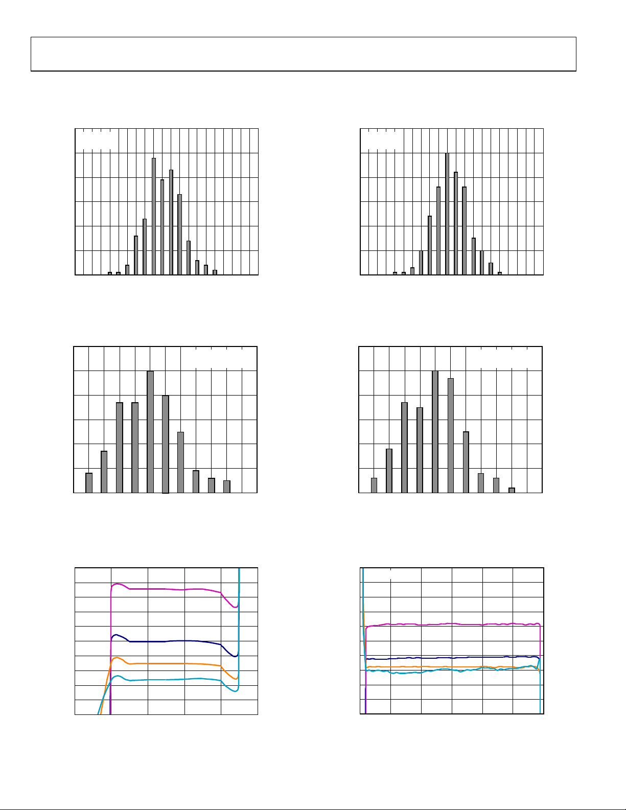
TYPICAL PERFORMANCE CHARACTERISTICS
TA = 25°C, unless otherwise noted.
Figure 5. Input Offset Voltage Distribution
Figure 6. Input Offset Voltage Drift Distribution
Figure 8. Input Offset Voltage Distribution
Figure 9. Input Offset Voltage Drift Distribution
Figure 7. Input Offset Voltage vs. Common-Mode Voltage
Figure 10. Input Offset Voltage vs. Common-Mode Voltage
Rev. C | Page 6 of 20

AD8622/AD8624
I
B
(pA)
07527-008
TEMPERATURE (°C)
–60
–50
–40
–30
–20
–10
0
–50 –25 0 25 50 75 100 125
IB+
IB–
VSY = ±2.5V
–150
–125
–100
–75
–50
–25
0
25
50
–2.5 –1.5 –0.5 0.5 1.5 2.5
VSY = ±2.5V
07527-012
VCM (V)
I
B
(pA)
10
1
0.1
0.01
0.001
0.01 0.1 1 10 100
LOAD CURRENT ( mA)
OUTPUT VOLTAGE TO SUPPLY RAIL (V)
07527-013
VSY = ±2.5V
VCC – V
OH
VOL – V
EE
07527-011
TEMPERATURE (°C)
I
B
(pA)
–50
–40
–30
–20
–10
0
10
–50 –25 0 25 50 75 100 125
IB+
I
B
–
VSY = ±15V
–60
–40
–20
0
20
40
60
–15 –10 –5 0 5 10 15
VSY = ±15V
07527-009
V
CM
(V)
I
B
(pA)
0.01 0.1 1 10 100
LOAD CURRENT ( mA)
OUTPUT VOLTAGE TO SUPPLY RAIL (V)
07527-010
VSY = ±15V
VCC – V
OH
VOL – V
EE
100
10
1
0.1
0.01
0.001
Figure 11. Input Bias Current vs. Temperature
Figure 12. Input Bias Current vs. Common-Mode Voltage
Figure 14. Input Bias Current vs. Temperature
Figure 15. Input Bias Current vs. Common-Mode Voltage
Figure 13. Output Voltage to Supply Rail vs. Load Current
Figure 16. Output Voltage to Supply Rail vs. Load Current
Rev. C | Page 7 of 20

AD8622/AD8624
0.06
0.05
0.04
0.03
0.02
0.01
0
–50 –25 0 25 50 75 100 125
TEMPERATURE (°C)
OUTPUT VOLTAGE TO SUPPLY RAIL (V)
07527-017
VSY = ±2.5V
R
L
= 10kΩ
V
CC
– V
OH
VOL – V
EE
0.30
0.25
0.20
0.15
0.10
0.05
0
0.35
–0.05
0 2 4 6 8 10 12 14 16 18
V
SY
(±V)
I
SY
(mA)
07527-044
+85°C
+25°C
–40°C
+125°C
100
80
60
40
20
0
–20
–40
100
80
60
40
20
0
–20
–40
1k 10k 100k 1M 10M
FREQUENCY ( Hz )
GAIN (dB)
PHASE (Degrees)
07527-018
VSY = ±2.5V
R
L
= 10kΩ
PHASE
GAIN
0.16
0.14
0.12
0.10
0.08
0.06
0.04
0.02
0
–50 –25 0 25 50 75 100 125
TEMPERATURE (°C)
OUTPUT VOLTAGE TO SUPPLY RAIL (V)
07527-014
V
CC
– V
OH
V
OL
– V
EE
V
SY
= ±15V
R
L
= 10kΩ
I
(mA)
100
80
60
40
20
0
–20
–40
100
80
60
40
20
0
–20
–40
1k 10k 100k 1M 10M
FREQUENCY ( Hz )
GAIN (dB)
PHASE (Degrees)
07527-015
VSY = ±15V
R
L
= 10kΩ
PHASE
GAIN
Figure 17. Output Voltage to Supply Rail vs. Temperature
Figure 18. Supply Current vs. Supply Voltage
Figure 20. Output Voltage to Supply Rail vs. Temperature
0.35
0.30
0.25
0.20
SY
0.15
0.10
0.05
VSY = ±15V
VSY = ±2.5V
25–25–50 500 75 100 125
TEMPERATURE (°C)
07527-045
Figure 21. Supply Current vs. Temperature
Figure 19. Open-Loop Gain and Phase vs. Frequency
Figure 22. Open-Loop Gain and Phase vs. Frequency
Rev. C | Page 8 of 20

AD8622/AD8624
60
50
40
30
20
10
0
–10
–20
–30
–40
100 1k 10k 100k 1M 10M
FREQUENCY ( Hz )
GAIN (dB)
07527-019
VSY = ±2.5V
R
L
= 10kΩ
AV = 100
AV = 10
AV = 1
10k
1k
100
10
1
0.1
100 1k 10k 100k 1M
FREQUENCY ( Hz )
Z
OUT
(Ω)
07527-023
VSY = ±2.5V
AV = 100
AV = 10
AV = 1
140
120
100
80
60
40
20
0
FREQUENCY ( Hz )
CMRR (dB)
07527-021
V
SY
= ±2.5V
10 100 1k 10k 100k 1M
60
50
40
30
20
10
0
–10
–20
–30
–40
100 1k 10k 100k 1M 10M
FREQUENCY ( Hz )
GAIN (dB)
07527-016
V
SY
= ±15V
R
L
= 10kΩ
A
V
= 100
A
V
= 10
AV = 1
10k
1k
100
10
1
0.1
100 1k 10k 100k 1M
FREQUENCY ( Hz )
Z
OUT
(Ω)
07527-020
V
SY
= ±15V
AV = 100
AV = 10
AV = 1
140
120
100
80
60
40
20
0
10 100 1k 10k 100k 1M
FREQUENCY ( Hz )
CMRR (dB)
07527-024
V
SY
= ±15V
Figure 23. Closed-Loop Gain vs. Frequency
Figure 24. Output Impedance vs. Frequency
Figure 26. Closed-Loop Gain vs. Frequency
Figure 27. Output Impedance vs. Frequency
Figure 25. CMRR vs. Frequency
Figure 28. CMRR vs. Frequency
Rev. C | Page 9 of 20

AD8622/AD8624
120
100
80
60
40
20
0
10 100 1k 10k 100k 1M
FREQUENCY ( Hz )
PSRR (dB)
07527-025
VSY = ±2.5V
PSRR+
PSRR–
50
45
40
35
25
15
5
30
20
10
0
0.01 0.1 1 10 100
CAPACITANCE (nF)
OVERSHOOT (%)
07527-029
VSY = ±2.5V
A
V
= 1
R
L
= 10kΩ
OS+
OS–
07527-030
TIME (40µ s/DIV)
VOLTAGE (500mV/DIV)
V
SY
= ±2.5V
A
V
= 1
R
L
= 10kΩ
C
L
= 100pF
120
100
80
60
40
20
0
10 100 1k 10k 100k 1M
FREQUENCY ( Hz )
PSRR (dB)
07527-022
V
SY
= ±15V
PSRR+
PSRR–
50
45
40
35
25
15
5
30
20
10
0
0.01 0.1 1 10 100
CAPACITANCE (nF)
OVERSHOOT (%)
07527-026
VSY = ±15V
A
V
= 1
R
L
= 10kΩ
OS+
OS–
07527-027
TIME (40µ s/DIV)
VOLTAGE (5V/DIV)
VSY = ±15V
A
V
= 1
R
L
= 10kΩ
C
L
= 100pF
Figure 29. PSRR vs. Frequency
Figure 30. Small-Signal Overshoot vs. Load Capacitance
Figure 32. PSRR vs. Frequency
Figure 33. Small-Signal Overshoot vs. Load Capacitance
Figure 31. Large-Signal Transient Response
Figure 34. Large-Signal Transient Response
Rev. C | Page 10 of 20

AD8622/AD8624
07527-031
TIME (10µ s/DIV)
VOLTAGE (50mV/DIV)
V
SY
= ±2.5V
A
V
= 1
R
L
= 10kΩ
C
L
= 100pF
07527-035
TIME (20µ s/DIV)
0.4
0.2
0
0
–1
–2
–3
INPUT VOLTAGE (V)
OUTPUT VOLTAGE (V)
VSY = ±2.5V
A
V
= –100
R
L
= 10kΩ
INPUT
OUTPUT
0.2
INPUT VOLTAGE (V)
07527-028
TIME (10µ s/DIV)
VOLTAGE (50mV/DIV)
V
SY
= ±15V
A
V
= 1
R
L
= 10kΩ
C
L
= 100pF
07527-032
TIME (20µ s/DIV)
0.4
0.2
0
0
–10
–20
INPUT VOLTAGE (V)
OUTPUT VOLTAGE (V)
VSY = ±15V
A
V
= –100
R
L
= 10kΩ
INPUT
OUTPUT
07527-033
TIME (20µ s/DIV)
0.2
0
–0.2
10
20
0
–10
–20
INPUT VOLTAGE (V)
OUTPUT VOLTAGE (V)
VSY = ±15V
A
V
= –100
R
L
= 10kΩ
INPUT
OUTPUT
Figure 35. Small-Signal Transient Response
Figure 36. Negative Overload Recovery
0
INPUT
Figure 38. Small-Signal Transient Response
Figure 39. Negative Overload Recovery
–0.2
VSY = ±2.5V
= –100
A
V
= 10kΩ
R
L
OUTPUT
TIME (20µ s/DIV)
Figure 37. Positive Overload Recovery
3
2
OUTPUT VOLTAGE (V)
1
0
–1
07527-036
Figure 40. Positive Overload Recovery
Rev. C | Page 11 of 20

AD8622/AD8624
12
10
8
6
4
2
0
0 5 10 15
0.1% 0.01%
20 25 30 35
SETTLING TIME (µs)
OUTPUT STEP (V)
07527-034
V
SY
= ±15V
A
V
= –1
100
10
1
1 10 100 1k
FREQUENCY ( Hz )
VOLTAGE NOISE DENSITY (nV/ Hz)
07527-042
V
SY
= ±2.5V
1
0.1
0.01
1 10 100 1k
FREQUENCY ( Hz )
CURRENT NOIS E DE NS ITY (pA/ Hz)
07527-057
V
SY
= ±2.5V
UNCORRELATED
RS1 = 0Ω
CORRELATED
RS1 = R
S2
R
S1
R
S2
12
10
8
6
4
2
0
0 5 10 15
0.1%
0.01%
20 25 30 35
SETTLING TIME (µs)
OUTPUT STEP (V)
07527-037
V
SY
= ±15V
A
V
= +1
100
10
1
1 10 100 1k
FREQUENCY ( Hz )
VOLTAGE NOISE DENSITY (nV Hz)
07527-039
VSY = ±15V
1
0.1
0.01
1 10 100 1k
FREQUENCY ( Hz )
CURRENT NOIS E DE NS ITY (pA/
Hz)
07527-056
VSY = ±15V
UNCORRELATED
RS1 = 0Ω
CORRELATED
RS1 = R
S2
R
S1
R
S2
Figure 41. Output Step vs. Settling Time
Figure 42. Voltage Noise Density vs. Frequency
Figure 44. Output Step vs. Settling Time
Figure 45. Voltage Noise Density vs. Frequency
Figure 43. Current Noise Density vs. Frequency
Figure 46. Current Noise Density vs. Frequency
Rev. C | Page 12 of 20

AD8622/AD8624
07527-043
TIME (1s/DIV)
INPUT NOISE VOLTAGE (50nV/DIV)
V
SY
= ±2.5V
1
0.1
0.01
0.001
0.0001
0.001 0.01 0.1 1 10
AMPLIT UDE ( V rms)
THD + N (%)
07527-049
VSY = ±2.5V
f = 1kHz
R
L
= 10kΩ
07527-040
TIME (1s/DIV)
INPUT NOISE VOLTAGE (50nV/DIV)
V
SY
= ±15V
1
0.1
0.01
0.001
0.0001
0.001 0.01 0.1 1 10
AMPLIT UDE ( V rms)
THD + N (%)
07527-046
VSY = ±15V
f = 1kHz
R
L
= 10kΩ
Figure 47. 0.1 Hz to 10 Hz Noise
Figure 48. THD + Noise vs. Amplitude
Figure 49. 0.1 Hz to 10 Hz Noise
Figure 50. THD + Noise vs. Amplitude
Rev. C | Page 13 of 20

AD8622/AD8624
0.1
0.01
0.001
0.0001
10 100 1k 10k 100k
FREQUENCY ( Hz )
THD + N (%)
07527-051
VSY = ±2.5V
R
L
= 10kΩ
V
IN
= 300mV rms
0
–20
–40
–60
–80
–100
–120
–140
10 100 1k 10k 100k
FREQUENCY ( Hz )
CHANNEL SEPARAT ION (dB)
07527-048
VSY = ±2.5V TO ±15V
R
L
= 10kΩ
A
V
= –100
100kΩ
1kΩ
R
L
0.1
0.01
0.001
0.0001
10 100 1k 10k 100k
FREQUENCY ( Hz )
THD + N (%)
07527-050
VSY = ±15V
R
L
= 10kΩ
V
IN
= 300mV rms
Figure 51. THD + Noise vs. Frequency
Figure 53. THD + Noise vs. Frequency
Figure 52. Channel Separation vs. Frequency
Rev. C | Page 14 of 20

AD8622/AD8624
AD862x
500Ω
500Ω
R1
R2
2
3
1
07527-055
07527-053
TIME (200µ s/DIV)
VOLTAGE (5V/DIV)
V
SY
= ±15V
V
OUT
V
IN
+15V
–15V
V2
V1
R1
10.1kΩ
R2
1MΩ
R3
10.1kΩ
R4
1MΩ
V
O
07527-054
NOTES
1. V
O
= 100(V2 – V1)
2. TYPI CAL: 0.01mV < |V2 – V 1| < 149.7mV
3. TYPI CAL: –14.97V < V
O
< +14.97V
4. USE MATCHED RESISTORS.
1/2
AD8622
+
–
+15V
–15V
1/2
AD8622
+
–
APPLICATIONS INFORMATION
INPUT PROTECTION
The maximum differential input voltage that can be applied to
the AD8622/AD8624 is determined by the internal diodes
connected across its inputs and series resistors at each input. These
internal diodes and series resistors limit the maximum
differential input voltage to ±10 V and are needed to prevent baseemitter junction breakdown from occurring in the input stage of
the AD8622/AD8624 when very large differential voltages are
applied. In addition, the internal resistors limit the currents that
flow through the diodes. However, in applications where large
differential voltages can be inadvertently applied to the device,
large currents may still flow through these diodes. In such a
case, external resistors must be placed at both inputs of the op
amp to limit the input currents to ±10 mA (see Figure 54).
Figure 54. Input Protection
PHASE REVERSAL
An undesired phenomenon, phase reversal (also known as
phase inversion) occurs in many op amps when one or both of
the inputs are driven beyond the specified input voltage range
(IVR), in effect reversing the polarity of the output. In some
cases, phase reversal can induce lockups and even cause
equipment damage as well as self destruction.
The AD8622/AD8624 amplifiers have been carefully designed to
prevent output phase reversal when both inputs are maintained
within the specified input voltage range. In addition, even if one
or both inputs exceed the input voltage range but remain within
the supply rails, the output still does not phase reverse. Figure 55
shows the input/output waveforms of the AD8622/AD8624
configured as a unity-gain buffer with a supply voltage of ±15 V.
Figure 55. No Phase Reversal
MICROPOWER INSTRUMENTATION AMPLIFIER
The AD8622 is a dual, high precision, rail-to-rail output op amp
operating at just 215 μA quiescent current per amplifier. Its
ultralow offset, offset drift, and voltage noise, combined with its
very low bias current and high common-mode rejection ratio
(CMRR), are ideally suited for high accuracy and micropower
instrumentation amplifier.
Figure 56 shows the classic 2-op-amp instrumentation amplifier
with four resistors using the AD8622. The key to high CMRR
for this instrumentation amplifier are resistors that are well
matched from both the resistive ratio and the relative drift. For
true difference amplification, matching of the resistor ratio is
very important, where R3/R4 = R1/R2. Assuming perfectly
matched resistors, the gain of the circuit is 1 + R2/R1, which is
approximately 100. Tighter matching of two op amps in one
package, like the AD8622, offers a significant boost in
performance over the classical 3-op-amp configuration. Overall,
the circuit only requires about 430 µA of supply current.
Figure 56. Micropower Instrumentation Amplifier
Rev. C | Page 15 of 20

AD8622/AD8624
V
SY
V
SY
V
SY
R6
9.9kΩR39.9kΩ
R5
9.9kΩR19.9kΩ
R2
9.9kΩ
R7
200Ω
R8
4.12kΩ
R9
98.8kΩ
R4
9.9kΩ
ADR121 – 2.5V
400Ω
×4
HALL
ELEMENT
V
OUT
= 2.5V + × MAGNETIC FIELD (mT)
55mV
mT
07527-052
+
–
+
–
V
SY
–
+
V
SY
AD862x
AD862x
AD862x
AD862x
–
+
+
C3
0.1µF
TO 10µF
C2
0.1µF
C1
1µF TO 10µF
NOTES
1. USE MATCHED RESISTO RS FOR IN-AMP.
2. FOR INFORMATION ON C1, C2, AND C3, REFE R TOADR121 DATA SHEET.
HALL SENSOR SIGNAL CONDITIONING
The AD8622/AD8624 is also highly suitable for high accuracy,
low power signal conditioning circuits. One such use is in Hall
sensor signal conditioning (see Figure 57). The magnetic
sensitivity of a Hall element is proportional to the bias voltage
applied across it. With 1 V bias voltage, the Hall element
consumes about 2.5 mA of supply current and has a sensitivity
of 5.5 mV/mT typical. To reduce power consumption, bias
voltage must be reduced, but at the risk of lower sensitivity. The
only way to achieve higher sensitivity is by introducing a gain
using a precision micropower amplifier. The AD8622/AD8624,
with all its features, is well suited to amplify the sensitivity of the
Hall element.
The ADR121 is a precision micropower 2.5 V voltage reference.
A precision voltage reference is required to hold a constant current
so that the Hall voltage only depends on the intensity of the mag-
netic field. Using the 4.12k:98.8k resistive divider, the bias
voltage of the Hall element is reduced to 100 mV, leading to only
250 µA of power consumption. The 3-op-amp in-amp
configuration of the AD8622/AD8624 then increases the
sensitivity to 55 m V /mT. The key to high CMRR for this in-amp
configuration are resistors that are well matched (where R1/R2
= R3/R4) from both the resistive ratio and relative drift. The
resistors are important in determining the performance over
manufacturing tolerances, time and temperature. At least 1% or
better resistors are recommended. Using the AD8622/AD8624 to
amplify the sensor signal can reduce power while also achieving
higher sensitivity. The total current consumed is just 1.2 mA,
resulting in 21× improvement in sensitivity/power.
Figure 57. Hall Sensor Signal Conditioning
Rev. C | Page 16 of 20

AD8622/AD8624
INPUT BIAS
CANCELLATION
CIRCUITRY
V
B1
V
B2
D1 D2
500Ω
500Ω
+IN x
V+
–IN x
V–
C1
Q11
OUT x
Q12
Q8
Q9
Q10
Q5
Q3
Q2Q1
Q4
Q6
Q7
D4
D3
R1
R3
R2
07527-062
SIMPLIFIED SCHEMATIC
Figure 58. Simplified Schematic
Rev. C | Page 17 of 20

AD8622/AD8624
COMPLIANT TO JEDEC STANDARDS MO-187-AA
100709-B
6°
0°
0.80
0.55
0.40
4
8
1
5
0.65 BSC
0.40
0.25
1.10 MAX
3.20
3.00
2.80
COPLANARITY
0.10
0.23
0.09
3.20
3.00
2.80
5.15
4.90
4.65
PIN 1
IDENTIFIER
15° MAX
0.95
0.85
0.75
0.15
0.05
CONTROLLING DIMENSIONSARE IN MI LLIMET E RS ; INCH DIMENSIONS
(IN PARENTHESES) ARE ROUNDED-OFF MILLIMETER EQUI
VALENTS FOR
REFERENCE O NLYAND ARE NOT APPROPRIATE FOR USE IN DESIGN.
COMPLIANT TO JEDEC STANDARDS MS-012-AA
012407-A
0.25 (0.0098)
0.17 (0.0067)
1.27 (0.0500)
0.40 (0.0157)
0.50 (0.0196)
0.25 (0.0099)
45°
8°
0°
1.75 (0.0688)
1.35 (0.0532)
SEATING
PLANE
0.25 (0.0098)
0.10 (0.0040)
4
1
8 5
5.00 (0.1968)
4.80 (0.1890)
4.00 (0.1574)
3.80 (0.1497)
1.27 (0.0500)
BSC
6.20 (0.2441)
5.80 (0.2284)
0.51 (0.0201)
0.31 (0.0122)
COPLANARITY
0.10
OUTLINE DIMENSIONS
Figure 59. 8-Lead Mini Small Outline Package [MSOP]
(RM-8)
Dimensions shown in millimeters
Figure 60. 8-Lead Standard Small Outline Package [SOIC_N]
Narrow Body
(R-8)
Dimensions shown in millimeters and (inches)
Rev. C | Page 18 of 20

AD8622/AD8624
2.70
2.60 SQ
2.50
COMPLIANT
TO
JEDEC STANDARDS MO-220-WGGC.
012909-B
1
0.65
BSC
BOTTOM VIEWTOP VIEW
16
5
8
9
12
13
4
EXPOSED
PAD
PIN 1
INDICATOR
4.10
4.00 SQ
3.90
0.45
0.40
0.35
SEATING
PLANE
0.80
0.75
0.70
0.05 MAX
0.02 NOM
0.20 REF
0.25 MIN
COPLANARITY
0.08
PIN 1
INDICATOR
0.35
0.30
0.25
FOR PROP E R CONNECTION O F
THE EXPOSED PAD, REFER TO
THE PIN CO NFIGURATION AND
FUNCTIO N DE S CRIPTIONS
SECTION OF THIS DATA SHEET.
COMPLI ANT TO JEDEC ST ANDARDS M O-153-AB-1
061908-A
8°
0°
4.50
4.40
4.30
14
8
7
1
6.40
BSC
PIN 1
5.10
5.00
4.90
0.65 BSC
0.15
0.05
0.30
0.19
1.20
MAX
1.05
1.00
0.80
0.20
0.09
0.75
0.60
0.45
COPLANARITY
0.10
SEATING
PLANE
Figure 61. 16-Lead Lead Frame Chip Scale Package [LFCSP_WQ]
4 mm × 4mm Body, Very Very Thin Quad
(CP-16-17)
Dimensions shown in millimeters
Figure 62. 14-Lead Thin Shrink Small Outline Package [TSSOP]
(RU-14)
Dimensions shown in millimeters
ORDERING GUIDE
Model1 Tempera ture Range Package Description Package Option Branding
AD8622ARMZ −40°C to +125°C 8-Lead MSOP RM-8 A1P
AD8622ARMZ-REEL −40°C to +125°C 8-Lead MSOP RM-8 A1P
AD8622ARMZ-R7 −40°C to +125°C 8-Lead MSOP RM-8 A1P
AD8622ARZ −40°C to +125°C 8-Lead SOIC_N R-8
AD8622ARZ-REEL −40°C to +125°C 8-Lead SOIC_N R-8
AD8622ARZ-REEL7 −40°C to +125°C 8-Lead SOIC_N R-8
AD8624ACPZ-R2 −40°C to +125°C 16-Lead LFCSP_WQ CP-16-17
AD8624ACPZ-R7 −40°C to +125°C 16-Lead LFCSP_WQ CP-16-17
AD8624ACPZ-RL −40°C to +125°C 16-Lead LFCSP_WQ CP-16-17
AD8624ARUZ −40°C to +125°C 14-Lead TSSOP RU-14
AD8624ARUZ-RL −40°C to +125°C 14-Lead TSSOP RU-14
1
Z = RoHS Compliant Part.
Rev. C | Page 19 of 20

AD8622/AD8624
NOTES
©2009–2011 Analog Devices, Inc. All rights reserved. Trademarks and
registered trademarks are the property of their respective owners.
D07527-0-6/11(C)
Rev. C | Page 20 of 20
 Loading...