

Page 1
Ultrafast, 4 ns
+
FEATURES
4 ns propagation delay at 5 V
Single-supply operation: 3 V to 5 V
100 MHz input
Latch function
APPLICATIONS
High speed timing
Clock recovery and clock distribution
Line receivers
Digital communications
Phase detectors
High speed sampling
Read channel detection
PCMCIA cards
Zero-crossing detector
High speed analog-to-digital converter (ADC)
Upgrade for LT1394 and LT1016 designs
Single-Supply Comparators
AD8611/AD8612
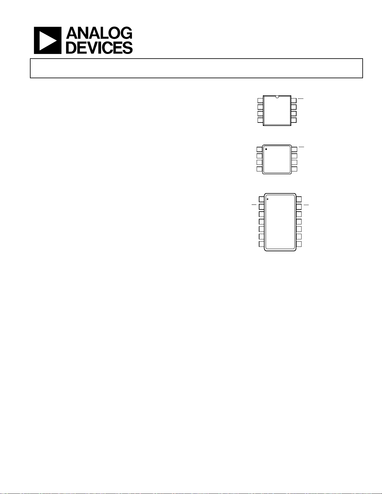
PIN CONFIGURATIONS
V+
1
AD8611
IN+
2
3
IN–
TOP VIEW
(Not to Scale)
4
V–
Figure 1. 8-Lead Narrow Body SOIC
V+
1
AD8611
IN+
2
TOP VIEW
IN–
3
(Not to Scale)
4
V–
Figure 2. 8-Lead MSOP
1
QA
2
QA
3
GND
LEA
V–
INA–
INA
AD8612
TOP VIEW
4
(Not to Scale)
5
6
7
Figure 3. 14-Lead TSSOP
(R-8)
(RM-8)
(RU-14)
8
7
6
5
8
7
6
5
QA
QA
GND
LATCH
QA
QA
GND
LATCH
14
QB
13
Q
12
GND
11
LEB
10
V+
9
INB–
8
INB+
06010-001
06010-002
B
06010-003
GENERAL DESCRIPTION
The AD8611/AD8612 are single and dual 4 ns comparators
with latch function and complementary output. The latch is not
functional if V
Fast 4 ns propagation delay makes the AD8611/AD8612 good
choices for timing circuits and line receivers. Propagation delays
for rising and falling signals are closely matched and tracked over
temperature. This matched delay makes the AD8611/AD8612
good choices for clock recovery because the duty cycle of the
output matches the duty cycle of the input.
Rev. A
Information furnished by Analog Devices is believed to be accurate and reliable. However, no
responsibility is assumed by Anal og Devices for its use, nor for any infringements of patents or ot her
rights of third parties that may result from its use. Specifications subject to change without notice. No
license is granted by implication or otherwise under any patent or patent rights of Analog Devices.
Trademarks and registered trademarks are the property of their respective owners.
is less than 4.3 V.
CC
The AD8611 has the same pinout as the LT1016 and LT1394,
with lower supply current and a wider common-mode input
range, which includes the negative supply rail.
The AD8611/AD8612 are specified over the industrial temperature range (−40°C to +85°C). The AD8611 is available in both
8-lead MSOP and narrow 8-lead SOIC surface-mount packages.
The AD8612 is available in a 14-lead TSSOP surface-mount
package.
One Technology Way, P.O. Box 9106, Norwood, MA 02062-9106, U.S.A.
Tel: 781.329.4700 www.analog.com
Fax: 781.461.3113 ©2006 Analog Devices, Inc. All rights reserved.
Page 2

AD8611/AD8612
TABLE OF CONTENTS
Features.............................................................................................. 1
Optimizing High Speed Performance..................................... 10
Applications....................................................................................... 1
Pin Configurations ........................................................................... 1
General Description ......................................................................... 1
Revision History ............................................................................... 2
Specifications..................................................................................... 3
Absolute Maximum Ratings............................................................ 5
Thermal Resistance ...................................................................... 5
ESD Caution.................................................................................. 5
Pin Configurations and Function Descriptions ........................... 6
Typical Performance Characteristics ............................................. 7
Applications..................................................................................... 10
REVISION HISTORY
8/06—Rev. 0 to Rev. A
Updated Format..................................................................Universal
Added No Latch if V
Changes to Pin Names.......................................................Universal
Added Pin Configurations and Function Descriptions Page..... 6
Changes to Table 8.......................................................................... 12
Changes to Figure 26...................................................................... 12
Changes to Ordering Guide.......................................................... 17
< 4.3 V .........................................Universal
CC
Upgrading the LT1394 and LT1016......................................... 10
Maximum Input Frequency and Overdrive............................ 10
Output Loading Considerations............................................... 11
Using the Latch to Maintain a Constant Output.................... 11
Input Stage and Bias Currents .................................................. 11
Using Hysteresis ......................................................................... 11
Clock Timing Recovery............................................................. 12
A 5 V, High Speed Window Comparator................................ 12
Outline Dimensions....................................................................... 16
Ordering Guide .......................................................................... 17
4/00—Revision 0: Initial Version
Rev. A | Page 2 of 20
Page 3

AD8611/AD8612
SPECIFICATIONS
V+ = 5.0 V, V− = V
Table 1.
Parameter Symbol Conditions Min Typ Max Unit
INPUT CHARACTERISTICS
Offset Voltage VOS 1 7 mV
−40°C ≤ TA ≤ +85°C 8 mV
Offset Voltage Drift ΔVOS/ΔT 4 μV/°C
Input Bias Current IB VCM = 0 V –6 –4 μA
I
Input Offset Current IOS VCM = 0 V ±4 μA
Input Common-Mode Voltage Range VCM 0.0 3.0 V
Common-Mode Rejection Ratio CMRR 0 V ≤ VCM ≤ 3.0 V 55 85 dB
Large Signal Voltage Gain AVO RL = 10 kΩ 3000 V/V
Input Capacitance CIN 3.0 pF
LATCH ENABLE INPUT
Logic 1 Voltage Threshold VIH VCC > 4.3 V 2.0 1.65 V
Logic 0 Voltage Threshold VIL VCC > 4.3 V 1.60 0.8 V
Logic 1 Current IIH VCC > 4.3 V, VLH = 3.0 V –1.0 –0.3 μA
Logic 0 Current IIL VCC > 4.3 V, VLL = 0.3 V –5 –2.7 μA
Latch Enable
Pulse Width t
Setup Time tS VCC > 4.3 V 0.5 ns
Hold Time tH VCC > 4.3 V 0.5 ns
DIGITAL OUTPUTS
Logic 1 Voltage VOH IOH = 50 μA, ΔVIN > 250 mV 3.0 3.35 V
Logic 1 Voltage VOH IOH = 3.2 mA, ΔVIN > 250 mV 2.4 3.4 V
Logic 0 Voltage VOL IOL = 3.2 mA, ΔVIN > 250 mV 0.25 0.4 V
DYNAMIC PERFORMANCE
Input Frequency f
Propagation Delay tP 200 mV step with 100 mV overdrive1 4.0 5.5 ns
−40°C ≤ TA ≤ +85°C 5 ns
Propagation Delay tP 100 mV step with 5 mV overdrive 5 ns
Differential Propagation Delay
(Rising Propagation Delay vs.
Falling Propagation Delay)
Rise Time 20% to 80% 2.5 ns
Fall Time 80% to 20% 1.1 ns
POWER SUPPLY
Power Supply Rejection Ratio PSRR 4.5 V ≤ V+ ≤ 5.5 V 55 73 dB
V+ Supply Current2 I+ 5.7 10 mA
−40°C ≤ TA ≤ +85°C 10
Ground Supply Current2 I
−40°C ≤ TA ≤ +85°C 7 mA
V− Supply Current2 I− 2.2 4 mA
−40°C ≤ TA ≤ +85°C 5 mA
1
Guaranteed by design.
2
Per comparator.
= 0 V, TA = 25°C, unless otherwise noted.
GND
−40°C ≤ TA ≤ +85°C –7 –4.5 μA
B
V
PW(E)
400 mV p-p sine wave 100 MHz
MAX
100 mV step with 100 mV overdrive
Δt
P
VO = 0 V, RL = ∞ 3.5 7 mA
GND
> 4.3 V 3 ns
CC
1
0.5 2.0 ns
Rev. A | Page 3 of 20
Page 4

AD8611/AD8612
V+ = 3.0 V, V− = VGND = 0 V, TA = 25°C, unless otherwise noted.
Table 2.
Parameter Symbol Conditions Min Typ Max Unit
INPUT CHARACTERISTICS
Offset Voltage VOS
Input Bias Current IB V
Input Common-Mode Voltage Range VCM
Common-Mode Rejection Ratio CMRR 0 V ≤ VCM ≤ 1.0 V 55
OUTPUT CHARACTERISTICS
Output High Voltage VOH I
Output Low Voltage VOL I
LATCH ENABLE INPUT Not functional if VCC < 4.3 V
POWER SUPPLY
Power Supply Rejection Ratio PSRR 2.7 V ≤ V+ ≤ 6 V
Supply Currents
V+ Supply Current
2
Ground Supply Current
2
V– Supply Current2 I−
DYNAMIC PERFORMANCE
Propagation Delay tP 100 mV step with 20 mV overdrive
1
Output high voltage without pull-up resistor. It may be useful to have a pull-up resistor to V+ for 3 V operation.
2
Per comparator.
3
Guaranteed by design.
= 0 V −6 −4.0
CM
IB −40°C ≤ TA ≤ +85°C −7 −4.5
0
1 7 mV
1.0 V
μA
μA
dB
= −3.2 mA, VIN > 250 mV 1.2
OH
= +3.2 mA, VIN > 250 mV
OL
1
V
0.3 V
VO = 0 V, RL = ∞
I+ −40°C ≤ TA ≤ +85°C
46
4.5 6.5 mA
dB
10 mA
I
−40°C ≤ TA ≤ +85°C
GND
2.5 3.5 mA
5.5 mA
−40°C ≤ TA ≤ +85°C
2 3.5 mA
4.8 mA
3
4.5 6.5 ns
Rev. A | Page 4 of 20
Page 5
AD8611/AD8612
ABSOLUTE MAXIMUM RATINGS
Table 3.
Parameter Rating
Total Analog Supply Voltage 7.0 V
Digital Supply Voltage 7.0 V
Input Voltage1 ±4 V
Differential Input Voltage ±5 V
Output Short-Circuit Duration to GND Indefinite
Storage Temperature Range
R, RU, RM Packages −65°C to +150°C
Operating Temperature Range −40°C to +85°C
Junction Temperature Range
R, RU, RM Packages −65°C to +150°C
Lead Temperature Range (Soldering, 10 sec) 300°C
1
The analog input voltage is equal to ±4 V or the analog supply voltage,
whichever is less.
Stresses above those listed under Absolute Maximum Ratings
may cause permanent damage to the device. This is a stress
rating only; functional operation of the device at these or any
other conditions above those indicated in the operational
section of this specification is not implied. Exposure to absolute
maximum rating conditions for extended periods may affect
device reliability.
THERMAL RESISTANCE
Table 4.
Package Type θ
8-Lead SOIC (R) 158 43 °C/W
8-Lead MSOP (RM) 240 43 °C/W
14-Lead TSSOP (RU) 240 43 °C/W
1
θJA is specified for the worst-case conditions, that is, a device in socket for
P-DIP and a device soldered in circuit board for SOIC and TSSOP.
1
θ
JA
Unit
JC
ESD CAUTION
ESD (electrostatic discharge) sensitive device. Electrostatic charges as high as 4000 V readily accumulate on
the human body and test equipment and can discharge without detection. Although this product features
proprietary ESD protection circuitry, permanent damage may occur on devices subjected to high energy
electrostatic discharges. Therefore, proper ESD precautions are recommended to avoid performance
degradation or loss of functionality.
Rev. A | Page 5 of 20
Page 6
AD8611/AD8612
+
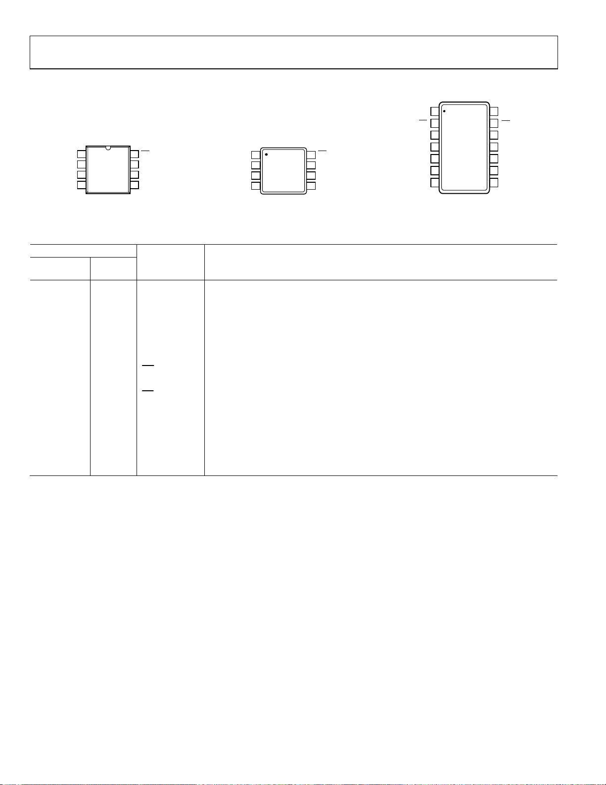
PIN CONFIGURATIONS AND FUNCTION DESCRIPTIONS
V+
IN+
IN–
V–
1
AD8611
2
3
TOP VIEW
(Not to Scale)
4
8
7
6
5
QA
QA
GND
LATCH
1
QA
2
QA
3
V–
AD8612
TOP VIEW
4
(Not to Scale)
5
6
7
GND
V+
1
AD8611
IN+
2
TOP VIEW
IN–
3
(Not to Scale)
4
06010-001
V–
8
7
6
5
QA
QA
GND
LATCH
06010-002
LEA
INA–
INA
14
QB
13
Q
B
12
GND
11
LEB
10
V+
9
INB–
8
INB+
Figure 4. 8-Lead Narrow Body SOIC Pin Configuration Figure 5. 8-L ead MS OP Pin Config uration Fig ure 6. 14-Lea d TSSO P Pin C onfigu ration
Table 5. Pin Function Descriptions
Pin No.
SOIC and
MSOP
TSSOP Mnemonic Description
1 10 V+ Positive Supply Terminal.
2 IN+ Noninverting Analog Input of the Differential Input Stage.
3 IN− Inverting Analog Input of the Differential Input Stage.
4 5 V− Negative Supply Terminal.
5 LATCH Latch Enable Input.
6 3, 12 GND Negative Logic Supply
7 1 QA One of Two Complementary Output for Channel A.
8 2
QA
One of Two Complementary Output for Channel A.
14 QB One of Two Complementary Output for Channel B.
13
QB
One of Two Complementary Output for Channel B.
4 LEA Channel A Latch Enable.
11 LEB Channel B Latch Enable.
7 INA+ Noninverting Analog Input of the Differential Input Stage for Channel A.
6 INA− Inverting Analog Input of the Differential Input Stage for Channel A.
8 INB+ Noninverting Analog Input of the Differential Input Stage for Channel B.
9 INB− Inverting Analog Input of the Differential Input Stage for Channel B.
06010-003
Rev. A | Page 6 of 20
Page 7

AD8611/AD8612
TYPICAL PERFORMANCE CHARACTERISTICS
8
V+ = 5V
OVERDRIVE > 10mV
7
6
5
4
3
2
PROPAGATI ON DELAY ( ns)
1
0
–50
Figure 7. Propagation Delay vs. Temperature
–25
PD–
PD+
0
TEMPERATURE ( °C)
25 50 75
100
06010-004
18
V+ = 5V
T
= 25°C
A
OVERDRIVE = 5mV
14
1.0
PD–
PD+
1.5 2.0
12
8
6
PROPAGATI ON DELAY (n s)
2
0
020.5
SOURCE RESISTANCE (kΩ)
Figure 10. Propagation Delay vs. Source Resistance
.5
6010-007
18
16
14
12
10
8
6
PROPAGATI ON DELAY (n s)
4
2
0
PD–
PD+
0
OVERDRIVE (mV)
Figure 8. Propagation Delay vs. Overdrive
8
V+ = 5V
T
= 25°C
A
7
OVERDRIVE > 10mV
6
5
4
3
2
PROPAGATION DELAY (n s)
1
0
0
CAPACIT ANCE (pF)
PD–
Figure 9. Propagation Delay vs. Load Capacitance
V+ = 5V
T
= 25°C
A
PD+
8
7
6
5
4
3
2
PROPAGATI ON DELAY (n s)
1
255 101520
06010-005
0
PD+
PD–
SUPPLY VOLTAGE (V)
TA = 25°C
STEP = 100mV
OVERDRIVE > 10mV
45
623
06010-008
Figure 11. Propagation Delay vs. Supply Voltage
35
TA = 25°C
STEP = 100mV
OVERDRIVE = 50mV
30
25
20
15
10
PROPAGATI ON DELAY (n s)
5
8020 40 60
06010-006
0
PD–
45
COMMON-MODE VOLTAGE (V)
PD+
623
06010-009
Figure 12. Propagation Delay vs. Common-Mode Voltage
Rev. A | Page 7 of 20
Page 8

AD8611/AD8612
1.2
1.0
0.8
(mV)
0.6
OS
V
0.4
0.2
40
35
30
25
(mA)
20
SY+
I
15
VS = 3V
= 5V
V
S
0
–60 100–40
–20 0 20406080
TEMPERATURE ( °C)
Figure 13. Offset Voltage vs. Temperature
V+ = 5V
T
=25°C
A
06010-010
0.40
0.35
0.30
0.25
–40°C
0.20
+85°C
0.15
+25°C
LOAD CURRENT (V )
0.10
0.05
0
01246810
SINK CURRENT (mA)
+85°C
+25°C
–40°C
2
6010-013
Figure 16. Output Low Voltage vs. Load Current (Sinking) Over Temperature
4.0
3.8
3.6
3.4
3.2
3.0
+85°C
+25°C
–40°C
10
5
0
INPUT FREQUENCY (MHz)
Figure 14. Supply Current vs. Input Frequency
2.0
V+ = 5V
1.8
1.6
1.4
1.2
1.0
0.8
TIMING (ns)
0.6
0.4
0.2
0
–50
–25
SETUP TIME
HOLD TIME
0
25 50 75
TEMPERATURE (°C)
Figure 15. Latch Setup and Hold Time vs. Temperature
100
2.8
OUTPUT HIGH VOLTAGE (V)
2.6
2.4
100110
06010-011
0
LOAD CURRENT (mA)
12246810
06010-014
Figure 17. Output High Voltage vs. Load Current (Sourcing) Over
Temperature
8
7
6
5
4
(mA)
SY
I
3
2
1
0
–60 100–40
06010-012
VS = 5V
VS = 3V
–20 0 20 40 60 80
TEMPERATURE (° C)
6010-015
Figure 18. Supply Current vs. Temperature
Rev. A | Page 8 of 20
Page 9

AD8611/AD8612
0
–0.5
–1.0
–1.5
–2.0
(mA)
–2.5
GND
I
–3.0
–3.5
–4.0
–4.5
50
Figure 19. I
V
= 3V
S
VS = 5V
0
TEMPERATURE (°C)
vs. Temperature
GND
50
100
06010-016
V+ = 5V
= 25°C
T
A
0V
VOLTAGE
–VIN TRACE @ 10mV/DIV
V
OUT
TRACE @ 1V/DIV
TIME (2ns/DIV)
Figure 22. Falling Edge Response
V
IN
V
OUT
6010-019
0
–0.5
–1.0
–40
V+ = 5V
= 25°C
T
A
VS = 3V
V
= 5V
S
–20
Figure 20. I
0 20406080
TEMPERATURE (°C)
− vs. Temperature
SY
V
OUT
V
IN
100
06010-017
–1.5
(mA)
SY
I
–2.0
–2.5
–3.0
–60
0V
VOLTAGE
V+ = 5V
T
= 25°C
A
0V
VOLTAGE
–VIN TRACE @ 10mV/DIV
V
OUT
V
OUT
V
IN
TRACE @ 1V/DIV
TIME (4ns/DIV)
Figure 23. Response to a 50 MHz, 100 mV Input Sine Wave
06010-020
–VIN TRACE @ 10mV/DIV
TRACE @ 1V/DIV
V
OUT
TIME (2ns/DIV)
06010-018
Figure 21. Rising Edge Response
Rev. A | Page 9 of 20
Page 10

AD8611/AD8612
APPLICATIONS
OPTIMIZING HIGH SPEED PERFORMANCE
As with any high speed comparator or amplifier, proper design
and layout of the AD8611/AD8612 should be used to ensure
optimal performance. Excess stray capacitance or improper
grounding can limit the maximum performance of high speed
circuitry.
Minimizing resistance from the source to the comparator’s
input is necessary to minimize the propagation delay of the
circuit. Source resistance in combination with the equivalent
input capacitance of the AD8611/AD8612 creates an R-C filter
that could cause a lagged voltage rise at the input to the
comparator. The input capacitance of the AD8611/AD8612 in
combination with stray capacitance from an input pin to
ground results in several picofarads of equivalent capacitance.
Using a surface-mount package and a minimum of input trace
length, this capacitance is typically around 3 pF to 5 pF. A
combination of 3 k source resistance and 3 pF of input
capacitance yields a time constant of 9 ns, which is slower than
the 4 ns propagation delay of the AD8611/AD8612. Source
impedances should be less than 1 k for best performance.
Another important consideration is the proper use of powersupply-bypass capacitors around the comparator. A 1 F bypass
capacitor should be placed within 0.5 inches of the device
between each power supply pin and ground. Another 10 nF
ceramic capacitor should be placed as close as possible to the
device in parallel with the 1 F bypass capacitor. The 1 F
capacitor reduces any potential voltage ripples from the power
supply, and the 10 nF capacitor acts as a charge reservoir for the
comparator during high frequency switching.
A continuous ground plane on the PC board is also
recommended to maximize circuit performance. A ground
plane can be created by using a continuous conductive plane
over the surface of the circuit board, only allowing breaks in the
plane for necessary traces and vias. The ground plane provides a
low inductive current return path for the power supply, thus
eliminating any potential differences at various ground points
throughout the circuit board caused from ground bounce. A
proper ground plane can also minimize the effects of stray
capacitance on the circuit board.
UPGRADING THE LT1394 AND LT1016
The AD8611 single comparator is pin-for-pin compatible with
the LT1394 and LT1016 and offers an improvement in propagation
delay over both comparators. These devices can easily be replaced
with the higher performance AD8611; however, there are differences, so it is useful to ensure that the system still operates properly.
The five major differences between the AD8611 and the LT1016
include input voltage range, input bias currents, propagation
delay, output voltage swing, and power consumption. Input
common-mode voltage is found by taking the average of the
Rev. A | Page 10 of 20
two voltages at the inputs to the comparator. The LT1016 has an
input voltage range from 1.25 V above the negative supply to
1.5 V below the positive supply. The AD8611 input voltage
range extends down to the negative supply voltage to within 2 V
of V+. If the input common-mode voltage is exceeded, input
signals should be shifted or attenuated to bring them into range,
keeping in mind the note about source resistance in the
Optimizing High Speed Performance section.
For example, an AD8611 powered from a 5 V single supply has
its noninverting input connected to a 1 V peak-to-peak, high
frequency signal centered around 2.3 V and its inverting input
connected to a fixed 2.5 V reference voltage. The worst-case
input common-mode voltage to the AD8611 is 2.65 V. This is
well below the 3.0 V input common-mode voltage range to the
comparator. Note that signals much greater than 3.0 V result in
increased input currents and may cause the comparator to
operate more slowly.
The input bias current to the AD8611 is 7 A maximum over
temperature (−40°C to +85°C). This is identical to the
maximum input bias current for the LT1394, and half of the
maximum I
and LT1394 flow out from the comparator’s inputs, as opposed
to the LT1016 whose input bias current flows into its inputs.
Using low value resistors around the comparator and low
impedance sources will minimize any potential voltage shifts
due to bias currents.
The AD8611 is able to swing within 200 mV of ground and
within 1.5 V of positive supply voltage. This is slightly more
output voltage swing than the LT1016. The AD8611 also uses
less current than the LT1016—5 mA as compared to 25 mA of
typical supply current.
The AD8611 has a typical propagation delay of 4 ns, compared
with the LT1394 and LT1016, whose propagation delays are
typically 7 ns and 10 ns, respectively.
for the LT1016. Input bias currents to the AD8611
B
MAXIMUM INPUT FREQUENCY AND OVERDRIVE
The AD8611 can accurately compare input signals up to
100 MHz with less than 10 mV of overdrive. The level of
overdrive required increases with ambient temperature, with up
to 50 mV of overdrive recommended for a 100 MHz input
signal and an ambient temperature of +85°C.
It is not recommend to use an input signal with a fundamental
frequency above 100 MHz because the AD8611 could draw up
to 20 mA of supply current and the outputs may not settle to a
definite state. The device returns to its specified performance
once the fundamental input frequency returns to below 100 MHz.
Page 11

AD8611/AD8612
V
R
OUTPUT LOADING CONSIDERATIONS
The AD8611 can deliver up to 10 mA of output current without
increasing its propagation delay. The outputs of the device
should not be connected to more than 40 TTL input logic gates
or drive less than 400 of load resistance.
The AD8611 output has a typical output swing between ground
and 1 V below the positive supply voltage. Decreasing the
output load resistance to ground lowers the maximum output
voltage due to the increase in output current.
Table 6 shows the
typical output high voltage vs. load resistance to ground.
Table 6. Maximum Output Voltage vs. Resistive Load
Output Load to Ground V+ − V
300 Ω 1.5 V
500 Ω 1.3 V
1 kΩ 1.2 V
10 kΩ 1.1 V
>20 kΩ 1.0 V
OUT, HI
(typ)
Connecting a 500 to 2 k pull-up resistor to V+ on the
output helps increase the output voltage so that it is closer to the
positive rail; in this configuration, however, the output voltage
will not reach its maximum until 20 ns to 50 ns after the output
voltage switches. This is due to the R-C time constant between
the pull-up resistor and the output and load capacitances. The
output pull-up resistor cannot improve propagation delay.
The AD8611 is stable with all values of capacitive load; however,
loading an output with greater than 30 pF increases the
propagation delay of that channel. Capacitive loads greater than
500 pF also create some ringing on the output wave.
Tabl e 7
shows propagation delay vs. several values of load capacitance.
The loading on one output of the AD8611 does not affect the
propagation delay of the other output.
Table 7. Propagation Delay vs. Capacitive Load
CL (pF) tPD Rising (ns) tPD Falling (ns)
<10 3.5 3.5
33 5 5
100 8 7
390 14.5 10
680 26 15
USING THE LATCH TO MAINTAIN A CONSTANT OUTPUT
With the VCC supply at a nominal 5 V, the latch input to the
AD8611/AD8612 can be used to retain data at the output of the
comparator. When the latch voltage goes high, the output
voltage remains in its previous state, independent of changes in
the input voltage.
The setup time for the AD8611/AD8612 is 0.5 ns and the hold
time is 0.5 ns. Setup time is defined as the minimum amount of
time the input voltage must remain in a valid state before the
latch is activated for the latch to function properly. Hold time is
defined as the amount of time the input must remain constant
after the latch voltage goes high for the output to remain latched
to its voltage.
The latch input is TTL and CMOS compatible, so a logic high is
a minimum of 2.0 V and a logic low is a maximum of 0.8 V. The
latch circuitry in the AD8611/AD8612 has no built-in
hysteresis. At or below approximately 4.1 V, the latch pin
becomes unresponsive and should normally be tied low for low
V
operation.
CC
INPUT STAGE AND BIAS CURRENTS
The AD8611 and AD8612 each use a bipolar PNP differential
input stage. This enables the input common-mode voltage range
to extend from within 2.0 V of the positive supply voltage to
200 mV below the negative supply voltage. Therefore, using a
single 5 V supply, the input common-mode voltage range is
−200 mV to +3.0 V. Input common-mode voltage is the average
of the voltages at the two inputs. For proper operation, the input
common-mode voltage should be kept within the commonmode voltage range.
The input bias current for the AD8611/AD8612 is 4 A, which
is the amount of current that flows from each input of the
comparator. This bias current goes to zero on an input that is
high and doubles on an input that is low, which is a characteristic
common to any bipolar comparator. Care should be taken in
choosing resistances to be connected around the comparator
because large resistors could significantly decrease the voltage
due to the input bias current.
The input capacitance for the AD8611/AD8612 is typically 3 pF.
This is measured by inserting a 5 kΩ source resistance in series
with the input and measuring the change in propagation delay.
USING HYSTERESIS
Hysteresis can easily be added to a comparator through the
addition of positive feedback. Adding hysteresis to a comparator
offers an advantage in noisy environments where it is undesirable
for the output to toggle between states when the input signal is
close to the switching threshold.
for configuring the AD8611 or AD8612 with hysteresis.
SIGNAL
REF
Figure 24. Configuring the AD8611/AD8612 with Hysteresis
In Figure 24, the input signal is connected directly to the
inverting input of the comparator. The output is fed back to the
noninverting input through R1 and R2. The ratio of R1 to
R1 + R2 establishes the width of the hysteresis window, with
V
setting the center of the window, or the average switching
REF
voltage. The QA or QB output switches low when the input
Figure 24 shows a simple method
COMPARATO
R1
R2
C
F
6010-021
Rev. A | Page 11 of 20
Page 12

AD8611/AD8612
V
V
voltage is greater than VHI, and does not switch high again until
the input voltage is less than V
()
−+=
5.1V
VV
R
×=
VV
REF
LO
+
where V+ is the positive supply voltage.
The capacitor C
is optional and can be added to introduce a
F
pole into the feedback network. This has the effect of increasing
the amount of hysteresis at high frequencies, which is useful
when comparing relatively slow signals in high frequency noise
environments. At frequencies greater than f
window approaches V
frequencies less than f
= V+ − 1.5 V and VLO = 0 V. For
HI
, the threshold voltages remain as in
P
Equation 1.
CLOCK TIMING RECOVERY
Comparators are often used in digital systems to recover clock
timing signals. High speed square waves transmitted over any
distance, even tens of centimeters, can become distorted due to
stray capacitance and inductance. Poor layout or improper
termination can also cause reflections on the transmission line,
further distorting the signal waveform. A high speed
comparator can be used to recover the distorted waveform
while maintaining a minimum of delay.
Figure 25 shows V
65 MHz, 100 mV peak-to-peak distorted clock signal into a 4 V
peak-to-peak square wave. The lower trace is the input to the
AD8611, and the upper trace is the QA or QB output from the
comparator. The AD8611 is powered from a 5 V single supply.
vs. VIN as the AD8611 is used to recover a
OUT
, as given in Equation 1:
LO
1
R
V
+
REFREFHI
21
RR
+
212RR
(1)
, the hysteresis
P
A 5 V, HIGH SPEED WINDOW COMPARATOR
A window comparator circuit is used to detect when a signal is
between two fixed voltages. The AD8612 can be used to create a
high speed window comparator, as shown in
example, the reference window voltages are set as:
2
R
=
V
HI
+
V
LO
21
RR
4
R
=
RR
+
The output of the A1 comparator goes high when the input
signal exceeds V
V
drops below VLO. When the input voltage is between VHI
IN
and V
, both comparator outputs are low, turning off both Q1
LO
and Q2, thus driving V
, and the output of A2 goes high only when
HI
to a high state. If the input signal
OUT
goes outside of the reference voltage window, V
To ensure a minimum of switching delay, the use of high speed
transistors is recommended for Q1 and Q2. Using the AD8612
with 2N3960 transistors provides a total propagation delay from
V
IN
to V
of less than 10 ns.
OUT
Table 8. Window Comparator Output States
V
Input Voltage
OUT
≈ 200 mV VIN < VLO
+5 V VLO < VIN < VHI
≈ 200 mV VIN > VHI
5V
R1
V
R2
V
IN
5V
HI
6
10
1kΩ
1
A1
7
3
AD8612
4
500Ω
Figure 26. In this
43
OUT
5
Q1
Q2
goes low.
1kΩ
V
OUT
OUT
V
5V
R3
V
2V/DIV
20mV/DIV
IN
LO
R4
NOTES
1. Q1, Q 2 = 2N3960.
2. PINS 2 AND 13 ARE NO CO NNECTS.
9
8
AD8612
A2
11
5
1kΩ
14
12
500Ω
6010-023
Figure 26. A High Speed Window Comparator
TIME (10n s/DIV)
06010-022
Figure 25. Using the AD8611 to Recover a Noisy Clock Signal
Rev. A | Page 12 of 20
Page 13

AD8611/AD8612
SPICE Model
* AD8611 SPICE Macro-Model Typical Values
* 1/2000, Ver. 1.0
* TAM/ADSC
*
* Node assignments
* non-inverting input
* | inverting input
* | | positive supply
* | | | negative supply
* | | | | Latch
* | | | | | DGND
* | | | | | | Q
* | | | | | | | QNOT
* | | | | | | | |
.SUBCKT AD8611 1 2 99 50 80 51 45 65
*
* INPUT STAGE
*
*
Q1 4 3 5 PIX
Q2 6 2 5 PIX
IBIAS 99 5 800E-6
RC1 4 50 1E3
RC2 6 50 1E3
CL1 4 6 3E-13
CIN 1 2 3E-12
VCM1 99 7 DC 1.9
D1 5 7 DX
EOS 3 1 POLY(1) (31,98) 1E-3 1
*
* Reference Voltages
*
EREF 98 0 POLY(2) (99,0) (50,0) 0 0.5 0.5
RREF 98 0 100E3
*
Rev. A | Page 13 of 20
Page 14

AD8611/AD8612
* CMRR = 66dB, ZERO AT 1 kHz
*
ECM1 30 98 POLY(2) (1,98) (2,98) 0 0.5 0.5
RCM1 30 31 10E3
RCM2 31 98 5
CCM1 30 31 15.9E-9
*
* Latch Section
*
RX 80 51 100E3
E1 10 98 (4,6) 1
S1 10 11 (80,51) SLATCH1
R2 11 12 1
C3 12 98 5 4E-12
E2 13 98 (12,98) 1
R3 12 13 500
*
* Power Supply Section
*
GSY1 99 52 POLY(1) (99,50) 4E-3 -2 6E-4
GSY2 52 50 POLY(1) (99,50) 3 7E-3 -.6E-3
RSY 52 51 10
*
* Gain Stage Av = 250 fp=100 MHz
*
G2 98 20 (12,98) 0.25
R1 20 98 1000
C1 20 98 10E-13
E3 97 0 (99,0) 1
E4 52 0 (51,0) 1
V1 97 21 DC 0.8
V2 22 52 DC 0.8
D2 20 21 DX
D3 22 20 DX
*
* Q Output
*
Rev. A | Page 14 of 20
Page 15

AD8611/AD8612
Q3 99 41 46 NOX
Q4 47 42 51 NOX
RB1 43 41 2000
RB2 40 42 2000
CB1 99 41 0.5E-12
CB2 42 51 1E-12
RO1 46 44 1
D4 44 45 DX
RO2 47 45 500
EO1 97 43 (20,51) 1
EO2 40 51 (20,51) 1
*
* Q NOT Output
*
Q5 99 61 66 NOX
Q6 67 62 51 NOX
RB3 63 61 2000
RB4 60 62 2000
CB3 99 61 0 5E-12
CB4 62 51 1E-12
RO3 66 64 1
D5 64 65 DX
RO4 67 65 500
EO3 63 51 (20,51) 1
EO4 97 60 (20,51) 1
*
* MODELS
*
.MODEL PIX PNP(BF=100,IS=1E-16)
.MODEL NOX NPN(BF=100,VAF=130,IS=1E-14)
.MODEL DX D(IS=1E-14)
.MODEL SLATCH1 VSWITCH(ROFF=1E6,RON=500,
+VOFF=2.1,VON=1.4)
.ENDS AD8611
Rev. A | Page 15 of 20
Page 16

AD8611/AD8612
OUTLINE DIMENSIONS
3.20
3.00
2.80
8
5
3.20
3.00
2.80
1
5.15
4.90
4.65
4
4.00 (0.1574)
3.80 (0.1497)
5.00 (0.1968)
4.80 (0.1890)
85
6.20 (0.2440)
5.80 (0.2284)
41
PIN 1
0.65 BSC
0.95
0.85
0.75
0.15
0.38
0.00
0.22
COPLANARITY
0.10
COMPLIANT TO JEDEC STANDARDS MO-187-AA
1.10 MAX
SEATING
PLANE
0.23
0.08
8°
0°
Figure 27. 8-Lead Mini Small Outline Package [MSOP]
(RM-8)
Dimensions shown in millimeters
4.50
4.40
4.30
PIN 1
1.05
1.00
0.80
Figure 29. 14-Lead Thin Shrink Small Outline Package [TSSOP]
0.25 (0.0098)
0.10 (0.0040)
0.80
0.60
0.40
5.10
5.00
4.90
14
0.65
BSC
0.15
0.05
COMPLIANT TO JEDEC STANDARDS MO-153-AB-1
0.30
0.19
8
6.40
BSC
71
1.20
MAX
SEATING
PLANE
COPLANARITY
0.20
0.09
0.10
COPLANARITY
CONTROLLING DIMENSIONS ARE IN MILLIMETERS; INCH DIMENSIONS
(IN PARENTHESES) ARE ROUNDED-OFF MILLIMETER EQUIVALENTS FOR
REFERENCE ONLY AND ARE NOT APPROPRIATE FOR USE IN DESIGN.
(RU-14)
Dimensions shown in millimeters
1.27 (0.0500)
BSC
0.10
SEATING
PLANE
COMPLIANT TO JEDEC STANDARDS MS-012-AA
1.75 (0.0688)
1.35 (0.0532)
0.51 (0.0201)
0.31 (0.0122)
0.25 (0.0098)
0.17 (0.0067)
0.50 (0.0196)
0.25 (0.0099)
8°
1.27 (0.0500)
0°
0.40 (0.0157)
Figure 28. 8-Lead Standard Small Outline Package [SOIC_N]
Narrow Body
(R-8)
Dimensions shown in millimeters and (inches)
8°
0°
0.75
0.60
0.45
× 45°
Rev. A | Page 16 of 20
Page 17

AD8611/AD8612
ORDERING GUIDE
Temperature
Model
Range
AD8611ARM-REEL –40°C to +85°C 8-Lead Mini Small Outline Package [MSOP] RM-8 G1A
AD8611ARM-R2 –40°C to +85°C 8-Lead Mini Small Outline Package [MSOP] RM-8 G1A
AD8611ARMZ-REEL1 –40°C to +85°C 8-Lead Mini Small Outline Package [MSOP] RM-8 G1A
AD8611ARMZ-R2
1
–40°C to +85°C 8-Lead Mini Small Outline Package [MSOP] RM-8 G1A
AD8611AR –40°C to +85°C 8-Lead Standard Small Outline Package [SOIC_N] R-8
AD8611AR-REEL –40°C to +85°C 8-Lead Standard Small Outline Package [SOIC_N] R-8
AD8611AR-REEL7 –40°C to +85°C 8-Lead Standard Small Outline Package [SOIC_N] R-8
AD8611ARZ1 –40°C to +85°C 8-Lead Standard Small Outline Package [SOIC_N] R-8
AD8611ARZ-REEL
1
–40°C to +85°C 8-Lead Standard Small Outline Package [SOIC_N] R-8
AD8611ARZ-REEL71 –40°C to +85°C 8-Lead Standard Small Outline Package [SOIC_N] R-8
AD8612ARU –40°C to +85°C 14-Lead Thin Shrink Small Outline Package [TSSOP] RU-14
AD8612ARU-REEL –40°C to +85°C 14-Lead Thin Shrink Small Outline Package [TSSOP] RU-14
AD8612ARUZ
1
–40°C to +85°C 14-Lead Thin Shrink Small Outline Package [TSSOP] RU-14
AD8612ARUZ-REEL1 –40°C to +85°C 14-Lead Thin Shrink Small Outline Package [TSSOP] RU-14
1
Z = Pb-free part.
Package Description Package Option Branding
Rev. A | Page 17 of 20
Page 18

AD8611/AD8612
NOTES
Rev. A | Page 18 of 20
Page 19

AD8611/AD8612
NOTES
Rev. A | Page 19 of 20
Page 20

AD8611/AD8612
NOTES
©2006 Analog Devices, Inc. All rights reserved. Trademarks and
registered trademarks are the property of their respective owners.
C06010-0-8/06(A)
Rev. A | Page 20 of 20
 Loading...