

Page 1
Precision CMOS, Single-Supply, Rail-to-Rail,
Input/Output Wideband Operational Amplifiers
FEATURES
Low offset voltage: 500 μV maximum
Single-supply operation: 2.7 V to 5.5 V
Low supply current: 750 μA/Amplifier
Wide bandwidth: 8 MHz
Slew rate: 5 V/μs
Low distortion
No phase reversal
Low input currents
Unity-gain stable
Qualified for automotive applications
APPLICATIONS
Current sensing
Barcode scanners
PA controls
Battery-powered instrumentation
Multipole filters
Sensors
ASIC input or output amplifiers
Audio
GENERAL DESCRIPTION
The AD8601, AD8602, and AD8604 are single, dual, and quad
rail-to-rail, input and output, single-supply amplifiers featuring
very low offset voltage and wide signal bandwidth. These amplifiers
use a new, patented trimming technique that achieves superior
performance without laser trimming. All are fully specified to
operate on a 3 V to 5 V single supply.
The combination of low offsets, very low input bias currents,
and high speed make these amplifiers useful in a wide variety
of applications. Filters, integrators, diode amplifiers, shunt
current sensors, and high impedance sensors all benefit from
the combination of performance features. Audio and other ac
applications benefit from the wide bandwidth and low distortion.
For the most cost-sensitive applications, the D grades offer this
ac performance with lower dc precision at a lower price point.
Applications for these amplifiers include audio amplification for
portable devices, portable phone headsets, bar code scanners,
portable instruments, cellular PA controls, and multipole filters.
The ability to swing rail-to-rail at both the input and output
enables designers to buffer CMOS ADCs, DACs, ASICs, and
other wide output swing devices in single-supply systems.
AD8601/AD8602/AD8604
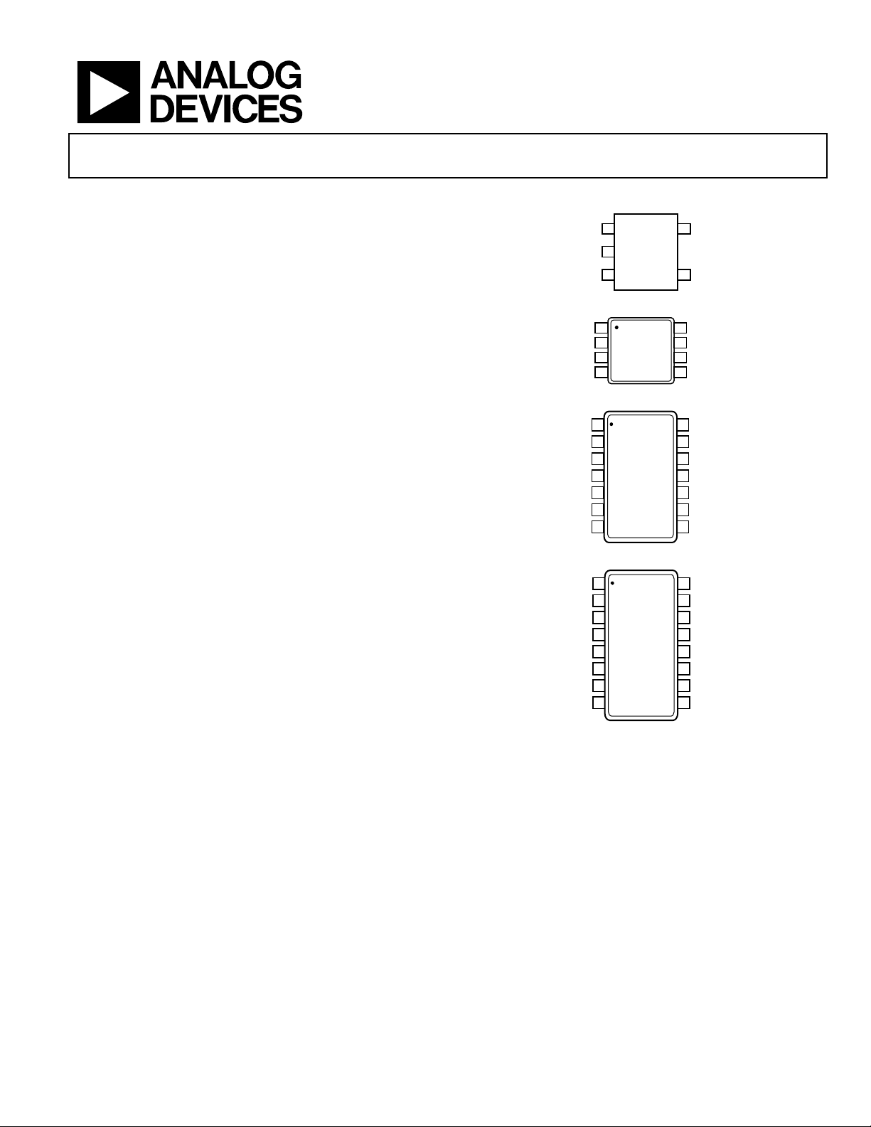
PIN CONFIGURATIONS
OUT A
1
AD8601
TOP VIEW
V–
2
(Not to S cale)
+IN
3
Figure 1. 5-Lead SOT-23 (RJ Suffix)
OUT A
1
AD8602
2
–IN A
+IN A
V–
TOP VIEW
3
(Not to S cal e)
4
Figure 2. 8-Lead MSOP (RM Suffix) and 8-Lead SOIC (R-Suffix)
1
OUT A
2
–IN A
3
+IN A
+IN B
–IN B
OUT B
V+
AD8604
TOP VIEW
4
(Not to Scale)
5
6
7
Figure 3. 14-Lead TSSOP (RU Suffix) and 14-Lead SOIC (R Suffix)
1
OUT A
2
–IN A
3
+IN A
+IN B
–IN B
OUT B
NC NC
AD8604
TOP VIEW
4
V+
(Not to Scale)
5
6
7
8
NC = NO CONNECT
Figure 4. 16-Lead Shrink Small Outline QSOP (RQ Suffix)
The AD8601, AD8602, and AD8604 are specified over the
extended industrial (−40°C to +125°C) temperature range. The
AD8601, single, is available in a tiny, 5-lead SOT-23 package. The
AD8602, dual, is available in 8-lead MSOP and 8-lead, narrow
SOIC surface-mount packages. The AD8604, quad, is available
in 14-lead TSSOP, 14-lead SOIC, and 16-lead QSOP packages.
See the Ordering Guide for automotive grades.
5
4
8
7
6
5
14
13
12
11
10
9
8
16
15
14
13
12
11
10
9
V+
–IN
V+
OUT B
–IN B
+IN B
OUT D
–IN D
+IN D
V–
+IN C
–IN C
OUT C
OUT D
–IN D
+IN D
V–
+IN C
–IN C
OUT C
01525-001
01525-002
01525-003
01525-004
Rev. G
Rev. G
Information furnished by Analog Devices is believed to be accurate and reliable. However, no
Information furnished by Analog Devices is believed to be accurate and reliable. However, no
responsibility is assumed by Analog Devices for its use, nor for any infringements of patents or other
responsibility is assumed by Analog Devices for its use, nor for any infringements of patents or other
rights of third parties that may result from its use. Specifications subject to change without notice. No
rights of third parties that may result from its use. Specifications subject to change without notice. No
license is granted by implication or otherwise under any patent or patent rights of Analog Devices.
license is granted by implication or otherwise under any patent or patent rights of Analog Devices.
Trademarks and registered trademarks are the property of their respective owners.
Trademarks and registered trademarks are the property of their respective owners.
One Technology Way, P.O. Box 9106, Norwood, MA 02062-9106, U.S.A.
One Technology Way, P.O. Box 9106, Norwood, MA 02062-9106, U.S.A.
Tel: 781.329.4700 www.analog.com
Tel: 781.329.4700 www.analog.com
Fax: 781.461.3113 ©2000–2011 Analog Devices, Inc. All rights reserved.
Fax: 781.461.3113 ©2000–2011 Analog Devices, Inc. All rights reserved.
Page 2

AD8601/AD8602/AD8604
TABLE OF CONTENTS
Features.............................................................................................. 1
Applications....................................................................................... 1
General Description ......................................................................... 1
Pin Configurations ........................................................................... 1
Revision History ............................................................................... 2
Specifications..................................................................................... 3
Electrical Characteristics ............................................................. 3
Absolute Maximum Ratings............................................................ 5
Thermal Resistance ...................................................................... 5
ESD Caution.................................................................................. 5
Typical Performance Characteristics ............................................. 6
Theory of Operation ...................................................................... 15
Rail-to-Rail Input Stage............................................................. 15
REVISION HISTORY
1/11—Rev. F to Rev. G
Changes to Ordering Guide.......................................................... 22
Change to Automotive Products Section .................................... 22
5/10—Rev. E to Rev. F
Changes to Features Section and General Description
Section................................................................................................ 1
Changes to Ordering Guide.......................................................... 22
Added Automotive Products Section .......................................... 22
2/10—Rev. D to Rev. E
Add 16-Lead QSOP............................................................Universal
Changes to Table 3 and Table 4....................................................... 5
Updated Outline Dimensions....................................................... 19
Changes to Ordering Guide.......................................................... 22
Input Overvoltage Protection................................................... 16
Overdrive Recovery ................................................................... 16
Power-On Time.......................................................................... 16
Using the AD8602 in High Source Impedance
Applications ................................................................................ 16
High Side and Low Side, Precision Current Monitoring ...... 16
Using the AD8601 in Single-Supply, Mixed Signal
Applications ................................................................................ 17
PC100 Compliance for Computer Audio Applications ........ 17
SPICE Model............................................................................... 18
Outline Dimensions....................................................................... 19
Ordering Guide .......................................................................... 22
Automotive Products................................................................. 22
11/03—Rev. C to Rev. D
Changes to Features ..........................................................................1
Changes to Ordering Guide.............................................................4
3/03—Rev. B to Rev. C
Changes to Features ..........................................................................1
3/03—Rev. A to Rev. B
Change to Features............................................................................1
Change to Functional Block Diagrams...........................................1
Change to TPC 39 .......................................................................... 11
Changes to Figures 4 and 5 ........................................................... 14
Changes to Equations 2 and 3................................................. 14, 15
Updated Outline Dimensions....................................................... 16
Rev. G | Page 2 of 24
Page 3

AD8601/AD8602/AD8604
SPECIFICATIONS
ELECTRICAL CHARACTERISTICS
VS = 3 V, VCM = VS/2, TA = 25°C, unless otherwise noted.
Table 1.
A Grade D Grade
Parameter Symbol Conditions Min Typ Max Min Typ Max Unit
INPUT CHARACTERISTICS
Offset Voltage (AD8601/AD8602) VOS 0 V ≤ VCM ≤ 1.3 V 80 500 1100 6000 μV
−40°C ≤ TA ≤ +85°C 700 7000 μV
−40°C ≤ TA ≤ +125°C 1100 7000 μV
0 V ≤ VCM ≤ 3 V1 350 750 1300 6000 μV
−40°C ≤ TA ≤ +85°C 1800 7000 μV
−40°C ≤ TA ≤ +125°C 2100 7000 μV
Offset Voltage (AD8604) VOS VCM = 0 V to 1.3 V 80 600 1100 6000 μV
−40°C ≤ TA ≤ +85°C 800 7000 μV
−40°C ≤ TA ≤ +125°C 1600 7000 μV
V
= 0 V to 3.0 V1
CM
−40°C ≤ TA ≤ +85°C 2200 7000 μV
−40°C ≤ TA ≤ +125°C 2400 7000 μV
Input Bias Current IB 0.2 60 0.2 200 pA
−40°C ≤ TA ≤ +85°C 25 100 25 200 pA
−40°C ≤ TA ≤ +125°C 150 1000 150 1000 pA
Input Offset Current IOS 0.1 30 0.1 100 pA
−40°C ≤ TA ≤ +85°C 50 100 pA
−40°C ≤ TA ≤ +125°C 500 500 pA
Input Voltage Range 0 3 0 3 V
Common-Mode Rejection Ratio CMRR VCM = 0 V to 3 V 68 83 52 65 dB
Large Signal Voltage Gain AVO V
= 0.5 V to 2.5 V,
O
= 2 kΩ, VCM = 0 V
R
L
Offset Voltage Drift ΔVOS/ΔT 2 2 μV/°C
OUTPUT CHARACTERISTICS
Output Voltage High VOH IL = 1.0 mA 2.92 2.95 2.92 2.95 V
–40°C ≤ TA ≤ +125°C 2.88 2.88 V
Output Voltage Low VOL IL = 1.0 mA 20 35 20 35 mV
−40°C ≤ TA ≤ +125°C 50 50 mV
Output Current I
Closed-Loop Output Impedance Z
±30 ±30 mA
OUT
f = 1 MHz, AV = 1 12 12 Ω
OUT
POWER SUPPLY
Power Supply Rejection Ratio PSRR VS = 2.7 V to 5.5 V 67 80 56 72 dB
Supply Current/Amplifier ISY VO = 0 V 680 1000 680 1000 μA
−40°C ≤ TA ≤ +125°C 1300 1300 μA
DYNAMIC PERFORMANCE
Slew Rate SR RL = 2 kΩ 5.2 5.2 V/μs
Settling Time tS To 0.01% <0.5 <0.5 μs
Gain Bandwidth Product GBP 8.2 8.2 MHz
Phase Margin Φo 50 50 Degrees
NOISE PERFORMANCE
Voltage Noise Density en f = 1 kHz 33 33 nV/√Hz
f = 10 kHz 18 18 nV/√Hz
Current Noise Density in 0.05 0.05 pA/√Hz
1
For VCM between 1.3 V and 1.8 V, VOS may exceed specified value.
Rev. G | Page 3 of 24
350 800 1300 6000 μV
30 100 20 60 V/mV
Page 4

AD8601/AD8602/AD8604
VS = 5.0 V, VCM = VS/2, TA = 25°C, unless otherwise noted.
Table 2.
A Grade D Grade
Parameter Symbol Conditions Min Typ Max Min Typ Max Unit
INPUT CHARACTERISTICS
Offset Voltage (AD8601/AD8602) VOS 0 V ≤ VCM ≤ 5 V 80 500 1300 6000 μV
−40°C ≤ TA ≤ +125°C 1300 7000 μV
Offset Voltage (AD8604) VOS VCM = 0 V to 5 V 80 600 1300 6000 μV
−40°C ≤ TA ≤ +125°C 1700 7000 μV
Input Bias Current IB 0.2 60 0.2 200 pA
−40°C ≤ TA ≤ +85°C 100 200 pA
−40°C ≤ TA ≤ +125°C 1000 1000 pA
Input Offset Current IOS 0.1 30 0.1 100 pA
−40°C ≤ TA ≤ +85°C 6 50 6 100 pA
−40°C ≤ TA ≤ +125°C 25 500 25 500 pA
Input Voltage Range 0 5 0 5 V
Common-Mode Rejection Ratio CMRR VCM = 0 V to 5 V 74 89 56 67 dB
Large Signal Voltage Gain AVO
= 0.5 V to 4.5 V,
V
O
= 2 kΩ, VCM = 0 V
R
L
Offset Voltage Drift ΔVOS/ΔT 2 2 μV/°C
OUTPUT CHARACTERISTICS
Output Voltage High VOH IL = 1.0 mA 4.925 4.975 4.925 4.975 V
I
= 10 mA 4.7 4.77 4.7 4.77 V
L
−40°C ≤ TA ≤ +125°C 4.6 4.6 V
Output Voltage Low VOL IL = 1.0 mA 15 30 15 30 mV
I
= 10 mA 125 175 125 175 mV
L
−40°C ≤ TA ≤ +125°C 250 250 mV
Output Current I
Closed-Loop Output Impedance Z
±50 ±50 mA
OUT
f = 1 MHz, AV = 1 10 10 Ω
OUT
POWER SUPPLY
Power Supply Rejection Ratio PSRR VS = 2.7 V to 5.5 V 67 80 56 72 dB
Supply Current/Amplifier I
V
SY
= 0 V 750 1200 750 1200 μA
O
−40°C ≤ TA ≤ +125°C 1500 1500 μA
DYNAMIC PERFORMANCE
Slew Rate SR RL = 2 kΩ 6 6 V/μs
Settling Time tS To 0.01% <1.0 <1.0 μs
Full Power Bandwidth BWp <1% distortion 360 360 kHz
Gain Bandwidth Product GBP 8.4 8.4 MHz
Phase Margin Φo 55 55 Degrees
NOISE PERFORMANCE
Voltage Noise Density en f = 1 kHz 33 33 nV/√Hz
f = 10 kHz 18 18 nV/√Hz
Current Noise Density in f = 1 kHz 0.05 0.05 pA/√Hz
30 80 20 60 V/mV
Rev. G | Page 4 of 24
Page 5
AD8601/AD8602/AD8604
ABSOLUTE MAXIMUM RATINGS
Table 3.
Parameter Rating
Supply Voltage 6 V
Input Voltage GND to VS
Differential Input Voltage ±6 V
Storage Temperature Range −65°C to +150°C
Operating Temperature Range −40°C to +125°C
Junction Temperature Range −65°C to +150°C
Lead Temperature Range (Soldering, 60 sec) 300°C
ESD 2 kV HBM
Stresses above those listed under Absolute Maximum Ratings
may cause permanent damage to the device. This is a stress
rating only; functional operation of the device at these or any
other conditions above those indicated in the operational
section of this specification is not implied. Exposure to absolute
maximum rating conditions for extended periods may affect
device reliability.
THERMAL RESISTANCE
θJA is specified for worst-case conditions, that is, a device
soldered onto a circuit board for surface-mount packages using
a standard 4-layer board.
Table 4. Thermal Resistance
Package Type θJA θ
5-Lead SOT-23 (RJ) 190 92 °C/W
8-Lead SOIC (R) 120 45 °C/W
8-Lead MSOP (RM) 142 45 °C/W
14-Lead SOIC (R) 115 36 °C/W
14-Lead TSSOP (RU) 112 35 °C/W
16-Lead QSOP (RQ) 115 36 °C/W
Unit
JC
ESD CAUTION
Rev. G | Page 5 of 24
Page 6
AD8601/AD8602/AD8604
TYPICAL PERFORMANCE CHARACTERISTICS
3,000
2,500
VS = 3V
T
= 25°C
A
V
= 0V TO 3V
CM
60
50
VS = 5V
T
= 25°C TO 85°C
A
2,000
1,500
1,000
QUANTITY (Amplifiers)
500
0
–1.0 –0.8 –0.6 –0.4 –0.2 0 0.2 0.4 0.6 0.8 1.0
INPUT OFFSET VOLTAGE (mV)
Figure 5. Input Offset Voltage Distribution
3,000
VS = 5V
T
= 25°C
A
V
= 0V TO 5V
CM
2,500
2,000
1,500
1,000
QUANTITY (Amplifiers)
500
40
30
20
QUANTITY (Amplifiers)
10
0
012345678910
01525-005
TCVOS (µV/°C)
01525-008
Figure 8. Input Offset Voltage Drift Distribution
1.5
VS = 3V
= 25°C
T
A
1.0
0.5
0
–0.5
–1.0
INPUT OFFSET VOLTAGE (mV)
–1.5
0
–1.0 –0.8 –0.6 –0.4 –0.2 0 0.2 0.4 0.6 0.8 1.0
INPUT OFFSET VOLTAGE (mV)
Figure 6. Input Offset Voltage Distribution
60
50
40
30
20
QUANTITY ( Amp lifiers)
10
0
012345678910
TCVOS (µV/°C)
VS = 3V
T
= 25°C TO 85°C
A
Figure 7. Input Offset Voltage Drift Distribution
–2.0
0 0.5 1.0 1.5 2.0 2.5 3.0
01525-006
COMMON-MO DE VO LTAGE (V)
01525-009
Figure 9. Input Offset Voltage vs. Common-Mode Voltage
1.5
VS = 5V
= 25°C
T
A
1.0
0.5
0
–0.5
–1.0
INPUT OFFSET VOLTAGE (mV)
–1.5
–2.0
01234
01525-007
COMMON-MODE VOLTAGE ( V)
5
01525-010
Figure 10. Input Offset Voltage vs. Common-Mode Voltage
Rev. G | Page 6 of 24
Page 7
AD8601/AD8602/AD8604
300
VS = 3V
250
30
VS = 3V
25
200
150
100
INPUT BIAS CURRENT (pA)
50
0
–40 –25 –105 203550658095110125
TEMPERATURE ( °C)
Figure 11. Input Bias Current vs. Temperature
300
VS = 5V
250
200
150
100
INPUT BIAS CURRENT (pA)
50
20
15
10
INPUT OFF SE T CURRENT (pA)
5
0
–40 –25 –105 203550658095110125
01525-011
TEMPERATURE ( °C)
01525-014
Figure 14. Input Offset Current vs. Temperature
30
VS = 5V
25
20
15
10
INPUT OFF SE T CURRENT (pA)
5
0
–40 –25 –105 203550658095110125
TEMPERATURE ( °C)
Figure 12. Input Bias Current vs. Temperature
5
VS = 5V
= 25°C
T
A
4
3
2
INPUT BIAS CURRENT (pA)
1
0
0 0.5 1.0 1.5 2.0 2.5 3.0 3.5 4.0 4.5 5.0
COMMON-MODE VOLTAGE (V)
Figure 13. Input Bias Current vs. Common-Mode Voltage
0
–40 –25 –105 203550658095110125
01525-012
TEMPERATURE ( °C)
01525-015
Figure 15. Input Offset Current vs. Temperature
10k
VS = 2.7V
= 25°C
T
A
1k
100
SOURCE
10
OUTPUT VOLTAGE (mV)
1
0.1
0.001 0.01 0.1 1 10 100
01525-013
LOAD CURRENT (mA)
SINK
01525-016
Figure 16. Output Voltage to Supply Rail vs. Load Current
Rev. G | Page 7 of 24
Page 8
AD8601/AD8602/AD8604
10k
VS = 5V
T
= 25°C
A
1k
35
30
25
VS = 2.7V
100
10
OUTPUT VOLTAGE (mV)
1
0.1
0.001 0.01 0.1 1 10 100
SOURCE
SINK
LOAD CURRENT (mA)
Figure 17. Output Voltage to Supply Rail vs. Load Current
5.1
VS = 5V
5.0
VOH @ 1mA LOAD
4.9
4.8
VOH @ 10mA LOAD
4.7
OUTPUT VOLTAGE (V)
4.6
4.5
–40 –25 –105 203550658095110125
TEMPERATURE (°C)
Figure 18. Output Voltage Swing vs. Temperature
250
VS = 5V
200
150
VOH @ 10mA LOAD
100
OUTPUT VOLTAGE (mV)
50
VOH @ 1mA LOAD
0
–40 –25 –10 5 20 35 50 65 80 95 110 125
TEMPERATURE (°C)
Figure 19. Output Voltage Swing vs. Temperature
20
15
10
OUTPUT VOLTAGE (mV)
5
0
–40 –25 –10 5 20 35 50 65 80 95 110 125
01525-017
VOH @ 1mA LOAD
TEMPERATURE ( °C)
01525-020
Figure 20. Output Voltage Swing vs. Temperature
2.67
VS = 2.7V
2.66
2.65
VOH @ 1mA LOAD
2.64
OUTPUT VOLTAGE (V)
2.63
2.62
–40 –25 –10 5 20 35 50 65 80 95 110 125
01525-018
TEMPERATURE ( °C)
01525-021
Figure 21. Output Voltage Swing vs. Temperature
120
100
80
60
40
20
GAIN (dB)
0
–20
–40
–60
–80
1k 10k 100k 1M 10M 100M
01525-019
FREQUENCY (Hz)
PHASE
GAIN
VS = 3V
R
= NO LOAD
L
T
= 25°C
A
–90
–45
0
45
90
135
180
225
270
315
360
PHASE SHIFT (Degrees)
01525-022
Figure 22. Open-Loop Gain and Phase vs. Frequency
Rev. G | Page 8 of 24
Page 9

AD8601/AD8602/AD8604
120
100
80
60
40
20
GAIN (dB)
0
–20
–40
–60
–80
1k 10k 100k 1M 10M 100M
FREQUENCY (Hz)
GAIN
VS = 5V
R
= NO LOAD
L
T
= 25°C
A
PHASE
Figure 23. Open-Loop Gain and Phase vs. Frequency
VS = 3V
AV = 100
40
AV = 10
20
AV = 1
0
CLOSD-LOOP GAIN (dB)
T
= 25°C
A
–90
–45
0
45
90
135
180
225
270
315
360
PHASE SHIFT (Degrees)
01525-023
3.0
2.5
VS = 2.7V
V
= 2.6V p-p
IN
R
= 2kΩ
L
2.0
T
= 25°C
A
A
= 1
V
1.5
1.0
OUTPUT SWING (V p-p)
0.5
0
1k 10k 100k 1M 10M
FREQUENCY (Hz)
Figure 26. Closed-Loop Output Voltage Swing vs. Frequency
6
5
VS = 5V
V
= 4.9V p- p
IN
4
R
= 2kΩ
L
T
= 25°C
A
A
= 1
V
3
2
OUTPUT SWING (V p-p)
1
01525-026
1k 10k 100k 1M 10M 100M
FREQUENCY (Hz)
Figure 24. Closed-Loop Gain vs. Frequency
VS = 5V
T
= 25°C
AV = 100
40
AV = 10
20
AV = 1
0
CLOSD-LOOP GAIN (dB)
1k 10k 100k 1M 10M 100M
FREQUENCY (Hz)
A
Figure 25. Closed-Loop Gain vs. Frequency
0
01525-024
1k 10k 100k 1M 10M
FREQUENCY (Hz)
01525-027
Figure 27. Closed-Loop Output Voltage Swing vs. Frequency
200
VS = 3V
T
= 25°C
180
A
160
140
120
100
80
60
OUTPUT I M P EDANCE ( Ω)
40
20
0
01525-025
1k 10k 100k 1M 10M 100M
AV = 100
FREQUENCY (Hz)
AV = 10
AV = 1
01525-028
Figure 28. Output Impedance vs. Frequency
Rev. G | Page 9 of 24
Page 10

AD8601/AD8602/AD8604
200
VS = 5V
T
= 25°C
180
A
160
140
120
100
80
60
OUTPUT I M P EDANCE ( Ω)
40
20
0
100 1k 10k 100k 1M 10M
AV = 100
AV = 10
AV = 1
FREQUENCY (Hz)
Figure 29. Output Impedance vs. Frequency
160
VS = 3V
T
= 25°C
140
A
120
100
80
60
40
20
0
COMMON-MODE REJECTION (dB)
–20
–40
1k 10k 100k 1M 10M 20M
FREQUENCY (Hz)
Figure 30. Common-Mode Rejection Ratio vs. Frequency
160
VS = 5V
T
= 25°C
140
A
120
100
80
60
40
20
0
COMMON-MODE REJECTION (dB)
–20
–40
1k 10k 100k 1M 10M 20M
FREQUENCY (Hz)
Figure 31. Common-Mode Rejection Ratio vs. Frequency
01525-029
01525-030
01525-031
160
VS = 5V
T
= 25°C
140
A
120
100
80
60
40
20
0
POWER SUPP LY REJECTION (dB)
–20
–40
1k100 10k 100k 1M 10M
FREQUENCY (Hz)
Figure 32. Power Supply Rejection Ratio vs. Frequency
70
VS = 2.7V
R
=
L
∞
TA = 25°C
60
A
= 1
V
50
40
30
20
SMALL SIGNAL OVERSHOOT (%)
10
0
10 100 1k
CAPACITANCE (pF)
–OS
+OS
Figure 33. Small Signal Overshoot vs. Load Capacitance
70
VS = 5V
R
=
L
∞
TA = 25°C
60
A
= 1
V
50
40
30
20
SMALL SIGNAL OVERSHOOT (%)
10
0
10 100 1k
CAPACITANCE (pF)
–OS
+OS
Figure 34. Small Signal Overshoot vs. Load Capacitance
01525-032
01525-033
01525-034
Rev. G | Page 10 of 24
Page 11

AD8601/AD8602/AD8604
1.2
VS = 5V
1.0
0.8
0.6
0.4
0.2
SUPPLY CURRENT P ER AM P LIFIER ( mA)
0
–40 –25 –105 203550658095110125
TEMPERATURE (°C)
Figure 35. Supply Current per Amplifier vs. Temperature
1.0
VS = 3V
0.8
0.6
0.4
01525-035
0.1
VS = 5V
T
= 25°C
A
G = 10
0.01
G = 1
THD + N (%)
0.001
0.0001
20 100 1k 10k 20k
FREQUENCY (Hz)
RL = 600Ω
RL = 2kΩ
RL = 10kΩ
RL = 600Ω
RL = 10kΩ
Figure 38. Total Harmonic Distortion + Noise vs. Frequency
64
VS = 2.7V
= 25°C
T
A
56
48
40
32
24
RL = 2kΩ
01525-038
0.2
SUPPLY CURRENT P ER AM P LIFIER ( mA)
0
–40 –25 –105 203550658095110125
TEMPERATURE (°C)
Figure 36. Supply Current per Amplifier vs. Temperature
0.8
0.7
0.6
0.5
0.4
0.3
0.2
0.1
SUPPLY CURRENT P E R AM PLIFIER (mA)
0
012345
SUPPLY VOLTAGE (V)
Figure 37. Supply Current per Amplifier vs. Supply Voltage
01525-036
6
01525-037
16
VOLTAG E NOISE DENSITY (nV/ Hz)
8
0
0 5 10 15 20 25
FREQUENCY (kHz)
Figure 39. Voltage Noise Density vs. Frequency
208
VS = 2.7V
= 25°C
T
A
182
156
130
104
78
52
VOLTAG E NOISE DENSITY (nV/ Hz)
26
0
0 0.5 1.0 1.5 2.0 2.5
FREQUENCY (kHz)
Figure 40. Voltage Noise Density vs. Frequency
01525-039
01525-040
Rev. G | Page 11 of 24
Page 12

AD8601/AD8602/AD8604
208
182
156
130
104
VS = 5V
= 25°C
T
A
VS = 5V
T
= 25°C
A
78
52
VOLTAG E NOISE DENSITY (nV/ Hz)
26
0
0 0.5 1.0 1.5 2.0 2.5
FREQUENCY (kHz)
Figure 41. Voltage Noise Density vs. Frequency
64
VS = 5V
= 25°C
T
A
56
48
40
32
24
16
VOLTAG E NOISE DENSITY (nV/ Hz)
8
0
0 5 10 15 20 25
FREQUENCY (kHz)
Figure 42. Voltage Noise Density vs. Frequency
VOLTAGE (2.5µV/DIV)
TIME (1s/DIV)
01525-041
01525-044
Figure 44. 0.1 Hz to 10 Hz Input Voltage Noise
VS = 5V
= 10kΩ
R
L
= 200pF
C
L
= 25°C
T
A
50mV/DIV 200ns/DIV
01525-042
01525-045
Figure 45. Small Signal Transient Response
VS = 2.7V
= 25°C
T
A
VOLTAGE (2.5µV/DIV)
TIME (1s/DIV)
Figure 43. 0.1 Hz to 10 Hz Input Voltage Noise
01525-043
Rev. G | Page 12 of 24
VS = 2.7V
R
= 10kΩ
L
C
= 200pF
L
T
= 25°C
A
50mV/DIV 200ns/DIV
Figure 46. Small Signal Transient Response
01525-046
Page 13

AD8601/AD8602/AD8604
VS = 5V
R
= 10kΩ
L
C
= 200pF
L
A
= 1
V
T
= 25°C
A
V
IN
V
OUT
VS = 5V
R
= 10kΩ
L
A
= 1
V
T
= 25°C
A
VOLTAGE (1V/DIV)
TIME ( 400ns/DIV)
Figure 47. Large Signal Transient Response
VS = 2.7V
R
= 10kΩ
L
C
= 200pF
L
A
= 1
V
T
= 25°C
A
VOLTAGE (500mV/DIV )
TIME ( 400ns/DIV)
Figure 48. Large Signal Transient Response
V
IN
V
OUT
VS = 2.7V
R
= 10kΩ
L
A
= 1
V
T
= 25°C
A
VOLTAGE (1V/DIV)
01525-047
TIME (2µs/DIV)
01525-050
Figure 50. No Phase Reversal
VS = 5V
= 10kΩ
R
L
= 2V p-p
V
O
= 25°C
T
A
V
+0.1%
ERROR
–0.1%
VOLTAGE (V)
ERROR
VIN TRACE – 0.5V/DIV
TRACE – 10mV/DIV
V
OUT
01525-048
TIME (100ns/DIV)
IN
V
OUT
01525-051
Figure 51. Settling Time
2.0
VS = 2.7V
T
= 25°C
A
1.5
1.0
0.5
0
0.1% 0.01%
VOLTAGE (1V/DIV)
TIME (2µs/DIV)
01525-049
Figure 49. No Phase Reversal
–0.5
OUTPUT SWING (V)
–1.0
–1.5
–2.0
300 350 400 450 500 550 600
0.1% 0.01%
SETTLING TIME (ns)
Figure 52. Output Swing vs. Settling Time
01525-052
Rev. G | Page 13 of 24
Page 14

AD8601/AD8602/AD8604
5
VS = 5V
T
= 25°C
4
A
3
2
1
0
–1
OUTPUT SWING (V)
–2
–3
–4
–5
0 200 400 600 800 1,000
0.1% 0.01%
0.1% 0.01%
SETTLING TIME (ns)
01525-053
Figure 53. Output Swing vs. Settling Time
Rev. G | Page 14 of 24
Page 15

AD8601/AD8602/AD8604
THEORY OF OPERATION
The AD8601/AD8602/AD8604 family of amplifiers are rail-to-rail
input and output, precision CMOS amplifiers that operate from
2.7 V to 5.0 V of the power supply voltage. These amplifiers use
Analog Devices, Inc., DigiTrim® technology to achieve a higher
degree of precision than available from most CMOS amplifiers.
DigiTrim technology is a method of trimming the offset voltage
of the amplifier after it has been assembled. The advantage in postpackage trimming lies in the fact that it corrects any offset voltages
due to the mechanical stresses of assembly. This technology is
scalable and used with every package option, including the 5-lead
SOT-23, providing lower offset voltages than previously achieved in
these small packages.
The DigiTrim process is completed at the factory and does not
add additional pins to the amplifier. All AD860x amplifiers are
available in standard op amp pinouts, making DigiTrim completely
transparent to the user. The AD860x can be used in any precision
op amp application.
The input stage of the amplifier is a true rail-to-rail architecture,
allowing the input common-mode voltage range of the op amp
to extend to both positive and negative supply rails. The voltage
swing of the output stage is also rail-to-rail and is achieved by
using an NMOS and PMOS transistor pair connected in a
common-source configuration. The maximum output voltage
swing is proportional to the output current, and larger currents
limit how close the output voltage can get to the supply rail,
which is a characteristic of all rail-to-rail output amplifiers.
With 1 mA of output current, the output voltage can reach
within 20 mV of the positive rail and within 15 mV of the
negative rail. At light loads of >100 kΩ, the output swings
within ~1 mV of the supplies.
The open-loop gain of the AD860x is 80 dB, typical, with a load
of 2 kΩ. Because of the rail-to-rail output configuration, the gain
of the output stage and the open-loop gain of the amplifier are
dependent on the load resistance. Open-loop gain decreases with
smaller load resistances. Again, this is a characteristic inherent
to all rail-to-rail output amplifiers.
RAIL-TO-RAIL INPUT STAGE
The input common-mode voltage range of the AD860x extends
to both the positive and negative supply voltages. This maximizes
the usable voltage range of the amplifier, an important feature
for single-supply and low voltage applications. This rail-to-rail
input range is achieved by using two input differential pairs, one
NMOS and one PMOS, placed in parallel. The NMOS pair is
active at the upper end of the common-mode voltage range, and
the PMOS pair is active at the lower end.
The NMOS and PMOS input stages are separately trimmed using
DigiTrim to minimize the offset voltage in both differential pairs.
Both NMOS and PMOS input differential pairs are active in a
500 mV transition region, when the input common-mode voltage
is between approximately 1.5 V and 1 V below the positive supply
voltage. The input offset voltage shifts slightly in this transition
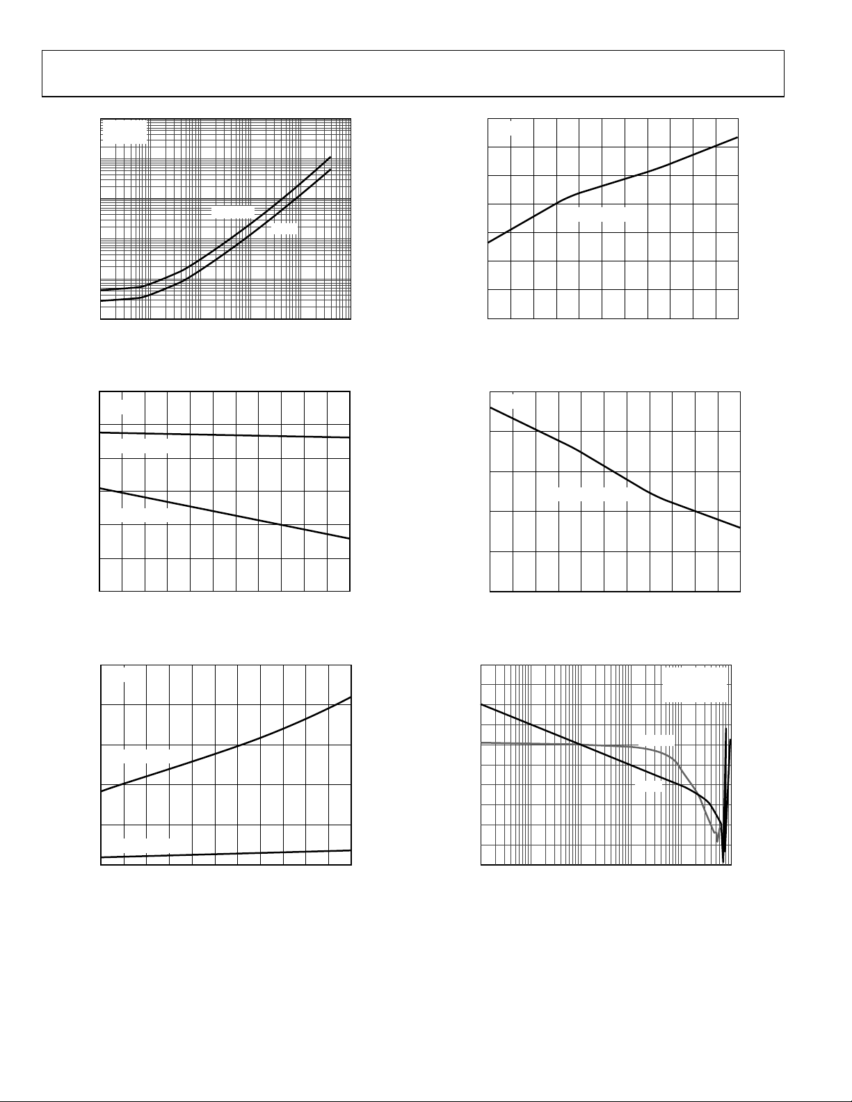
region, as shown in Figure 9 and Figure 10 .The common-mode
rejection ratio is also slightly lower when the input commonmode voltage is within this transition band. Compared to the
Burr-Brown OPA2340UR rail-to-rail input amplifier, shown in
Figure 54, the AD860x, shown in Figure 55, exhibits lower
offset voltage shift across the entire input common-mode
range, including the transition region.
0.7
0.4
0.1
–0.2
(mV)
OS
–0.5
V
–0.8
–1.1
–1.4
012345
Figure 54. Burr-Brown OPA2340UR Input Offset Voltage vs.
Common-Mode Voltage, 24 SOIC Units @ 25°C
V
(V)
CM
01525-054
0.7
0.4
0.1
–0.2
(mV)
OS
–0.5
V
–0.8
–1.1
–1.4
012345
Figure 55. AD8602AR Input Offset Voltage vs. Common-Mode Voltage,
300 SOIC Units @ 25°C
V
(V)
CM
01525-055
Rev. G | Page 15 of 24
Page 16

AD8601/AD8602/AD8604
F
V
INPUT OVERVOLTAGE PROTECTION
As with any semiconductor device, if a condition could exist
that could cause the input voltage to exceed the power supply,
the device’s input overvoltage characteristic must be considered.
Excess input voltage energizes the internal PN junctions in the
AD860x, allowing current to flow from the input to the supplies.
This input current does not damage the amplifier, provided it is
limited to 5 mA or less. This can be ensured by placing a resistor in
series with the input. For example, if the input voltage could
exceed the supply by 5 V, the series resistor should be at least
(5 V/5 mA) = 1 kΩ. With the input voltage within the supply
rails, a minimal amount of current is drawn into the inputs,
which, in turn, causes a negligible voltage drop across the series
resistor. Therefore, adding the series resistor does not adversely
affect circuit performance.
OVERDRIVE RECOVERY
Overdrive recovery is defined as the time it takes the output of
an amplifier to come off the supply rail when recovering from
an overload signal. This is tested by placing the amplifier in a
closed-loop gain of 10 with an input square wave of 2 V p-p
while the amplifier is powered from either 5 V or 3 V.
The AD860x has excellent recovery time from overload conditions.
The output recovers from the positive supply rail within 200 ns
at all supply voltages. Recovery from the negative rail is within
500 ns at a 5 V supply, decreasing to within 350 ns when the
device is powered from 2.7 V.
POWER-ON TIME
The power-on time is important in portable applications where
the supply voltage to the amplifier may be toggled to shut down
the device to improve battery life. Fast power-up behavior ensures
that the output of the amplifier quickly settles to its final voltage,
improving the power-up speed of the entire system. When the
supply voltage reaches a minimum of 2.5 V, the AD860x settles to
a valid output within 1 µs. This turn-on response time is faster
than many other precision amplifiers, which can take tens or
hundreds of microseconds for their outputs to settle.
USING THE AD8602 IN HIGH SOURCE IMPEDANCE APPLICATIONS
The CMOS rail-to-rail input structure of the AD860x allows
these amplifiers to have very low input bias currents, typically
0.2 pA. This allows the AD860x to be used in any application
that has a high source impedance or must use large value
resistances around the amplifier. For example, the photodiode
amplifier circuit shown in Figure 56 requires a low input bias
current op amp to reduce output voltage error. The AD8601
minimizes offset errors due to its low input bias current and low
offset voltage.
The current through the photodiode is proportional to the incident
light power on its surface. The 4.7 MΩ resistor converts this current
into a voltage, with the output of the AD8601 increasing at 4.7 V/µA.
The feedback capacitor reduces excess noise at higher frequencies
by limiting the bandwidth of the circuit to
BW
= (1)
1
()
Cπ
M7.42
F
Using a 10 pF feedback capacitor limits the bandwidth to
approximately 3.3 kHz.
10p
(OPTIONAL)
4.7MΩ
D1
AD8601
Figure 56. Amplifier Photodiode Circuit
V
OUT
4.7V/µA
01525-056
HIGH SIDE AND LOW SIDE, PRECISION CURRENT MONITORING
Because of its low input bias current and low offset voltage, the
AD860x can be used for precision current monitoring. The true
rail-to-rail input feature of the AD860x allows the amplifier to
monitor current on either the high side or the low side. Using both
amplifiers in an AD8602 provides a simple method for monitoring
both current supply and return paths for load or fault detection.
Figure 57 and Figure 58 demonstrate both circuits.
3
R2
MONITOR
OUTPUT
MONITOR
OUTPUT
249kΩ
Q1
2N3904
R1
100Ω
R
SENSE
0.1Ω
Figure 57. Low-Side Current Monitor
3V
R1
100Ω
Q1
2N3905
R2
2.49kΩ
Figure 58. High-Side Current Monitor
R
SENSE
0.1Ω
3V
1/2 AD8602
3V
1/2 AD8602
I
L
RETURN TO
GROUND
V+
01525-057
01525-058
Rev. G | Page 16 of 24
Page 17

AD8601/AD8602/AD8604
V
V
Voltage drop is created across the 0.1 Ω resistor that is
proportional to the load current. This voltage appears at the
inverting input of the amplifier due to the feedback correction
around the op amp. This creates a current through R1, which
in turn, pulls current through R2. For the low side monitor, the
monitor output voltage is given by
R
⎡
⎛
SENSE
×−=
R2VOutputMonitor 3 (2)
⎜
⎢
⎣
R1
⎝
⎤
⎞
I
×
⎟
L
⎥
⎠
⎦
For the high side monitor, the monitor output voltage is
R
SENSE
R1
⎞
I
(3)
⎟
L
⎠
⎛
R2OutputMonitor ×
×=
⎜
⎝
Using the components shown, the monitor output transfer
function is 2.5 V/A.
USING THE AD8601 IN SINGLE-SUPPLY, MIXED SIGNAL APPLICATIONS
Single-supply, mixed signal applications requiring 10 or more
bits of resolution demand both a minimum of distortion and a
maximum range of voltage swing to optimize performance. To
ensure that the ADCs or DACs achieve their best performance, an
amplifier often must be used for buffering or signal conditioning.
The 750 µV maximum offset voltage of the AD8601 allows the
amplifier to be used in 12-bit applications powered from a 3 V
single supply, and its rail-to-rail input and output ensure no
signal clipping.
Figure 59 shows the AD8601 used as an input buffer amplifier
to the AD7476, a 12-bit, 1 MSPS ADC. As with most ADCs,
total harmonic distortion (THD) increases with higher source
impedances. By using the AD8601 in a buffer configuration, the
low output impedance of the amplifier minimizes THD while
the high input impedance and low bias current of the op amp
minimizes errors due to source impedance. The 8 MHz gain
bandwidth product of the AD8601 ensures no signal attenuation up to 500 kHz, which is the maximum Nyquist frequency
for the AD7476.
REF193
0.1µF 0.1µF10µF
SCLK
SDATA
CS
SERIAL
INTERFACE
R
S
4
5
3
2
AD8601
1
680nF
1µF
TANT
V
DD
V
IN
GND
AD7476/AD7477
Figure 59. A Complete 3 V 12-Bit 1 MHz Analog-to-Digital Conversion System
5V
SUPPLY
µC/µP
01525-059
Figure 60 demonstrates how the AD8601 can be used as an
output buffer for the DAC for driving heavy resistive loads. The
AD5320 is a 12-bit DAC that can be used with clock frequencies
up to 30 MHz and signal frequencies up to 930 kHz. The railto-rail output of the AD8601 allows it to swing within 100 mV
of the positive supply rail while sourcing 1 mA of current. The
total current drawn from the circuit is less than 1 mA, or 3 mW
from a 3 V single supply.
3
3-WIRE
SERIAL
INTERFACE
1µF
4
5
6
AD5320
4
5
3
1
2
1
AD8601
V
OUT
0V TO 3 V
R
L
01525-060
Figure 60. Using the AD8601 as a DAC Output Buffer to Drive Heavy Loads
The AD8601, AD7476, and AD5320 are all available in spacesaving SOT-23 packages.
PC100 COMPLIANCE FOR COMPUTER AUDIO APPLICATIONS
Because of its low distortion and rail-to-rail input and output,
the AD860x is an excellent choice for low cost, single-supply
audio applications, ranging from microphone amplification
to line output buffering. Figure 38 shows the total harmonic
distortion plus noise (THD + N) figures for the AD860x. In
unity gain, the amplifier has a typical THD + N of 0.004%, or
−86 dB, even with a load resistance of 600 Ω. This is compliant
with the PC100 specification requirements for audio in both
portable and desktop computers.
Figure 61 shows how an AD8602 can be interfaced with an AC’97
codec to drive the line output. Here, the AD8602 is used as a
unity-gain buffer from the left and right outputs of the AC’97
codec. The 100 µF output coupling capacitors block dc current
and the 20 Ω series resistors protect the amplifier from short
circuits at the jack.
5
25
V
DD
V
29
DD
LEFT
35
OUT
AD1881
(AC’97)
RIGHT
36
OUT
26
V
SS
NOTES
1. ADDITIONAL PINS O M ITTED FOR CLARITY.
Figure 61. A PC100-Compliant Line Output Amplifier
5V
2
A
3
AD8602
5
B
6
AD8602
C1
+
2kΩ
C2
+
2kΩ
R4
20Ω
R2
R5
20Ω
R3
01525-061
8
100µF
1
4
100µF
7
Rev. G | Page 17 of 24
Page 18

AD8601/AD8602/AD8604
SPICE MODEL
The SPICE macro-model for the AD860x amplifier can be downloaded at www.analog.com. The model accurately simulates a
number of both dc and ac parameters, including open-loop gain,
bandwidth, phase margin, input voltage range, output voltage
swing vs. output current, slew rate, input voltage noise, CMRR,
PSRR, and supply current vs. supply voltage. The model is
optimized for performance at 27°C. Although it functions at
different temperatures, it may lose accuracy with respect to the
actual behavior of the AD860x.
Rev. G | Page 18 of 24
Page 19

AD8601/AD8602/AD8604
0
0
OUTLINE DIMENSIONS
3.00
2.90
2.80
1.30
1.15
0.90
.15 MAX
.05 MIN
1.70
1.60
1.50
5
123
4
1.90
BSC
0.50 MAX
0.35 MIN
COMPLIANT TO JEDEC STANDARDS MO-178-AA
0.95 BSC
1.45 MAX
0.95 MIN
3.00
2.80
2.60
SEATING
PLANE
0.20 MAX
0.08 MIN
10°
5°
0°
0.60
BSC
0.55
0.45
0.35
11-01-2010-A
Figure 62. 5-Lead Small Outline Transistor Package [SOT-23]
(RJ-5)
Dimensions shown in millimeters
3.20
3.00
2.80
8
5
4
0.40
0.25
5.15
4.90
4.65
1.10 MAX
15° MAX
6°
0°
0.23
0.09
0.80
0.55
0.40
10-07-2009-B
3.20
3.00
2.80
PIN 1
IDENTIFIER
0.95
0.85
0.75
0.15
0.05
COPLANARITY
1
0.65 BSC
0.10
COMPLIANT TO JEDEC STANDARDS MO-187-AA
Figure 63. 8-Lead Mini Small Outline Package [MSOP]
(RM-8)
Dimensions shown in millimeters
Rev. G | Page 19 of 24
Page 20

AD8601/AD8602/AD8604
4.00 (0.1574)
3.80 (0.1497)
0.25 (0.0098)
0.10 (0.0040)
COPLANARITY
0.10
CONTROLLING DIMENSIONS ARE IN MILLIMETERS; INCH DIMENSIONS
(IN PARENTHESES) ARE ROUNDED-OFF MILLIMETER EQUIVALENTS FOR
REFERENCE ONLYAND ARE NOT APPROPRIATE FOR USE IN DESIGN.
5.00(0.1968)
4.80(0.1890)
85
1
1.27 (0.0500)
SEATING
PLANE
COMPLIANT TO JEDEC STANDARDS MS-012-AA
BSC
6.20 (0.2441)
5.80 (0.2284)
4
1.75 (0.0688)
1.35 (0.0532)
0.51 (0.0201)
0.31 (0.0122)
8°
0°
0.25 (0.0098)
0.17 (0.0067)
0.50 (0.0196)
0.25 (0.0099)
1.27 (0.0500)
0.40 (0.0157)
45°
012407-A
Figure 64. 8-Lead Standard Small Outline Package [SOIC_N]
(R-8)
Dimensions shown in millimeters and (inches)
8.75 (0.3445)
8.55 (0.3366)
4.00 (0.1575)
3.80 (0.1496)
14
1
8
7
6.20 (0.2441)
5.80 (0.2283)
0.25 (0.0098)
0.10 (0.0039)
COPLANARITY
0.10
CONTROLLING DIME NSIONS ARE IN MILLIMETE RS; INCH DIMENSIO NS
(IN PARENTHESES) ARE ROUNDED-OFF MILLIMET E R E QUIVALENTS FOR
REFERENCE ONLYAND ARE NOT APPROP RIATE FOR USE IN DESIGN.
1.27 (0.0500)
BSC
0.51 (0.0201)
0.31 (0.0122)
COMPLIANT TO JEDEC S TANDARDS MS-012-AB
1.75 (0.0689)
1.35 (0.0531)
SEATING
PLANE
8°
0°
0.25 (0.0098)
0.17 (0.0067)
0.50 (0.0197)
0.25 (0.0098)
1.27 (0.0500)
0.40 (0.0157)
45°
060606-A
Figure 65. 14-Lead Standard Small Outline Package [SOIC_N]
(R-14)
Dimensions shown in millimeters and (inches)
Rev. G | Page 20 of 24
Page 21

AD8601/AD8602/AD8604
4.50
4.40
4.30
PIN 1
1.05
1.00
0.80
0.15
0.05
COPLANARITY
0.10
5.10
5.00
4.90
14
1
0.65 BSC
0.30
0.19
COMPLIANT TO JEDEC S T ANDARDS M O-153-AB-1
8
6.40
BSC
7
1.20
0.20
MAX
0.09
SEATING
PLANE
8°
0°
0.75
0.60
0.45
061908-A
Figure 66. 14-Lead Thin Shrink Small Outline Package [TSSOP]
(RU-14)
Dimensions shown in millimeters
0.197 (5.00)
0.193 (4.90)
0.189 (4.80)
0.065 (1.65)
0.049 (1.25)
0.010 (0.25)
0.004 (0.10)
COPLANARITY
0.004 (0.10)
16
1
0.025 (0.64)
BSC
CONTROLLING DIMENSIONS ARE IN INCHES; MILLIMETER DIMENSIONS
(IN PARENTHESES) ARE ROUNDED-OFF INCH EQUIVALENTSFOR
REFERENCE ONLYAND ARE NOT APPROPRIATE FOR USE IN DESIGN.
COMPLIANT TO JEDEC STANDARDS MO-137-AB
9
8
0.012 (0.30)
0.008 (0.20)
0.158 (4.01)
0.154 (3.91)
0.150 (3.81)
0.069 (1.75)
0.053 (1.35)
SEATING
PLANE
0.244 (6.20)
0.236 (5.99)
0.228 (5.79)
8°
0°
0.010 (0.25)
0.006 (0.15)
0.050 (1.27)
0.016 (0.41)
0.020 (0.51)
0.010 (0.25)
0.041 (1.04)
REF
01-28-2008-A
Figure 67. 16-Lead Shrink Small Outline Package [QSOP]
(RQ-16)
Dimensions shown in inches and (millimeters)
Rev. G | Page 21 of 24
Page 22

AD8601/AD8602/AD8604
ORDERING GUIDE
1, 2
Model
AD8601ARTZ-R2 −40°C to +125°C 5-Lead SOT-23 RJ-5 AAA
AD8601ARTZ-REEL −40°C to +125°C 5-Lead SOT-23 RJ-5 AAA
AD8601ARTZ-REEL7 −40°C to +125°C 5-Lead SOT-23 RJ-5 AAA
AD8601WARTZ-RL −40°C to +125°C 5-Lead SOT-23 RJ-5 AAA
AD8601WARTZ-R7 −40°C to +125°C 5-Lead SOT-23 RJ-5 AAA
AD8601WDRTZ-REEL −40°C to +125°C 5-Lead SOT-23 RJ-5 AAD
AD8601WDRTZ-REEL7 −40°C to +125°C 5-Lead SOT-23 RJ-5 AAD
AD8602AR −40°C to +125°C 8-Lead SOIC_N R-8
AD8602AR-REEL −40°C to +125°C 8-Lead SOIC_N R-8
AD8602AR-REEL7 −40°C to +125°C 8-Lead SOIC_N R-8
AD8602ARZ −40°C to +125°C 8-Lead SOIC_N R-8
AD8602ARZ-REEL −40°C to +125°C 8-Lead SOIC_N R-8
AD8602ARZ-REEL7 −40°C to +125°C 8-Lead SOIC_N R-8
AD8602WARZ-RL −40°C to +125°C 8-Lead SOIC_N R-8
AD8602WARZ-R7 −40°C to +125°C 8-Lead SOIC_N R-8
AD8602ARM-REEL −40°C to +125°C 8-Lead MSOP RM-8 ABA
AD8602ARMZ −40°C to +125°C 8-Lead MSOP RM-8 ABA
AD8602ARMZ-REEL −40°C to +125°C 8-Lead MSOP RM-8 ABA
AD8602DR −40°C to +125°C 8-Lead SOIC_N R-8
AD8602DR-REEL −40°C to +125°C 8-Lead SOIC_N R-8
AD8602DR-REEL7 −40°C to +125°C 8-Lead SOIC_N R-8
AD8602DRZ −40°C to +125°C 8-Lead SOIC_N R-8
AD8602DRZ-REEL −40°C to +125°C 8-Lead SOIC_N R-8
AD8602DRZ-REEL7 −40°C to +125°C 8-Lead SOIC_N R-8
AD8602DRM-REEL −40°C to +125°C 8-Lead MSOP RM-8 ABD
AD8602DRMZ-REEL −40°C to +125°C 8-Lead MSOP RM-8 ABD
AD8604ARZ −40°C to +125°C 14-Lead SOIC_N R-14
AD8604ARZ-REEL −40°C to +125°C 14-Lead SOIC_N R-14
AD8604ARZ-REEL7 −40°C to +125°C 14-Lead SOIC_N R-14
AD8604DRZ −40°C to +125°C 14-Lead SOIC_N R-14
AD8604DRZ-REEL −40°C to +125°C 14-Lead SOIC_N R-14
AD8604ARUZ −40°C to +125°C 14-Lead TSSOP RU-14
AD8604ARUZ-REEL −40°C to +125°C 14-Lead TSSOP RU-14
AD8604DRU −40°C to +125°C 14-Lead TSSOP RU-14
AD8604DRU -REEL −40°C to +125°C 14-Lead TSSOP RU-14
AD8604DRUZ −40°C to +125°C 14-Lead TSSOP RU-14
AD8604DRUZ-REEL −40°C to +125°C 14-Lead TSSOP RU-14
AD8604ARQZ −40°C to +125°C 16-Lead QSOP RQ-16
AD8604ARQZ-RL −40°C to +125°C 16-Lead QSOP RQ-16
AD8604ARQZ-R7 −40°C to +125°C 16-Lead QSOP RQ-16
1
Z = RoHS Compliant Part.
2
W = Qualified for Automotive Applications.
AUTOMOTIVE PRODUCTS
The AD8601W/AD8602W models are available with controlled manufacturing to support the quality and reliability requirements of
automotive applications. Note that these automotive models may have specifications that differ from the commercial models; therefore,
designers should review the Specifications section of this data sheet carefully. Only the automotive grade products shown are available for
use in automotive applications. Contact your local Analog Devices Account Representative for specific product ordering information and
to obtain the specific Automotive Reliability reports for these models.
Temperature Range Package Description Package Option Branding
Rev. G | Page 22 of 24
Page 23

AD8601/AD8602/AD8604
NOTES
Rev. G | Page 23 of 24
Page 24

AD8601/AD8602/AD8604
NOTES
©200–2011 Analog Devices, Inc. All rights reserved. Trademarks and
registered trademarks are the property of their respective owners.
D01525-0-1/11(G)
Rev. G | Page 24 of 24
 Loading...