Analog Devices AD8601 2 4 d Datasheet

Precision CMOS Single-Supply
14
13
12
11
10
9
8
1
2
3
4
5
6
7
ⴚIN A
ⴙIN A
Vⴙ
ⴙIN B
ⴚIN B
OUT B
OUT D
ⴚIN D
ⴙIN D
Vⴚ
ⴙIN C
ⴚIN C
OUT C
OUT A
AD8604
14
13
12
11
10
9
8
1
2
3
4
5
6
7
ⴚIN A
ⴙIN A
Vⴙ
ⴙIN B
ⴚIN B
OUT B
OUT D
ⴚIN D
ⴙIN D
Vⴚ
ⴙIN C
ⴚIN C
OUT C
OUT A
AD8604
Rail-to-Rail Input/Output Wideband
Operational Amplifiers
AD8601/AD8602/AD8604
FEATURES
Low Offset Voltage: 500 V Max
Single-Supply Operation: 2.7 V to 5.5 V
Low Supply Current: 750 A/Amplifier
Wide Bandwidth: 8 MHz
Slew Rate: 5 V/s
Low Distortion
No Phase Reversal
Low Input Currents
Unity Gain Stable
APPLICATIONS
Current Sensing
Barcode Scanners
PA Controls
Battery-Powered Instrumentation
Multipole Filters
Sensors
ASIC Input or Output Amplifiers
Audio
GENERAL DESCRIPTION
The AD8601, AD8602, and AD8604 are single, dual, and quad
rail-to-rail input and output single-supply amplifiers featuring very
low offset voltage and wide signal bandwidth. These amplifiers
use a new, patented trimming technique that achieves superior
performance without laser trimming. All are fully specified to
operate on a 3 V to 5 V single supply.
The combination of low offsets, very low input bias currents,
and high speed make these amplifiers useful in a wide variety of
applications. Filters, integrators, diode amplifiers, shunt current
sensors, and high impedance sensors all benefit from the combination of performance features. Audio and other ac applications
benefit from the wide bandwidth and low distortion. For the
most cost-sensitive applications, the D grades offer this ac performance with lower dc precision at a lower price point.
Applications for these amplifiers include audio amplification for
portable devices, portable phone headsets, bar code scanners,
portable instruments, cellular PA controls, and multipole filters.
The ability to swing rail-to-rail at both the input and output
enables designers to buffer CMOS ADCs, DACs, ASICs, and
other wide output swing devices in single-supply systems.
FUNCTIONAL BLOCK DIAGRAM
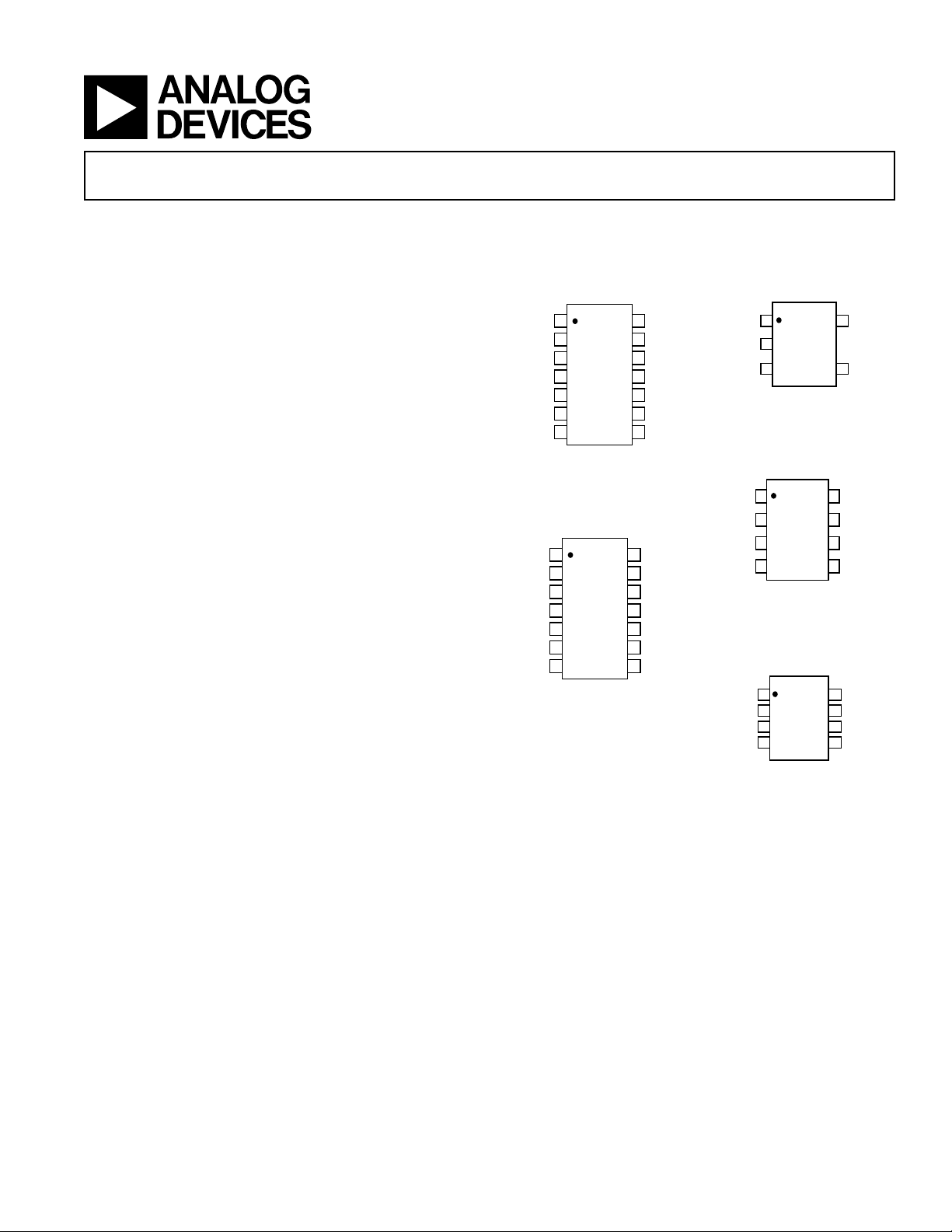
14-Lead TSSOP
(RU Suffix)
5-Lead SOT-23
(RT Suffix)
OUT A
1
Vⴚ
2
AD8601
ⴙIN
3
Vⴙ
5
ⴚIN
4
8-Lead MSOP
(RM Suffix)
14-Lead SOIC
(R Suffix)
1
OUT A
2
ⴚIN A
ⴙIN A
AD8602
3
VⴚⴙIN B
4
8
7
6
5
Vⴙ
OUT B
ⴚIN B
8-Lead SOIC
(R Suffix)
OUT A
ⴚIN A
ⴙIN A
Vⴚ
1
2
AD8602
3
4
8
7
6
5
Vⴙ
OUT B
ⴚIN B
ⴙIN B
The AD8601, AD8602, and AD8604 are specified over the
extended industrial (–40°C to +125°C) temperature range. The
AD8601, single, is available in the tiny 5-lead SOT-23 package.
The AD8602, dual, is available in 8-lead MSOP and narrow
SOIC surface-mount packages. The AD8604, quad, is available
in 14-lead TSSOP and narrow SOIC packages.
SOT, MSOP, and TSSOP versions are available in tape and
reel only.
REV. D
Information furnished by Analog Devices is believed to be accurate and
reliable. However, no responsibility is assumed by Analog Devices for its
use, nor for any infringements of patents or other rights of third parties that
may result from its use. No license is granted by implication or otherwise
under any patent or patent rights of Analog Devices. Trademarks and
registered trademarks are the property of their respective owners.
One Technology Way, P.O. Box 9106, Norwood, MA 02062-9106, U.S.A.
Tel: 781/329-4700 www.analog.com
Fax: 781/326-8703 © 2003 Analog Devices, Inc. All rights reserved.

AD8601/AD8602/AD8604–SPECIFICATIONS
ELECTRICAL CHARACTERISTICS
(VS = 3 V, VCM = VS/2, TA = 25ⴗC, unless otherwise noted.)
A Grade D Grade
Parameter Symbol Conditions Min Typ Max Min Typ Max Unit
INPUT CHARACTERISTICS
Offset Voltage (AD8601/AD8602) V
Offset Voltage (AD8604) V
Input Bias Current I
OS
OS
B
0 V ≤ VCM ≤ 1.3 V 80 500 1,100 6,000 µV
–40°C ≤ T
–40°C ≤ T
0 V ≤ VCM ≤ 3 V
–40°C ≤ T
–40°C ≤ T
≤ +85°C 700 7,000 µV
A
≤ +125°C 1,100 7,000 µV
A
*
≤ +85°C 1,800 7,000 µV
A
≤ +125°C 2,100 7,000 µV
A
350 750 1,300 6,000 µV
VCM = 0 V to 1.3 V 80 600 1,100 6,000 µV
–40°C ≤ T
–40°C ≤ T
VCM = 0 V to 3.0 V
–40°C ≤ T
–40°C ≤ T
≤ +85°C 800 7,000 µV
A
≤ +125°C 1,600 7,000 µV
A
A
A
*
350 800 1,300 6,000 µV
≤ +85°C 2,200 7,000 µV
≤ +125°C 2,400 7,000 µV
0.2 60 0.2 200 pA
–40°C ≤ T
≤ +85°C25100 25 200 pA
A
–40°C ≤ TA ≤ +125°C 150 1,000 150 1,000 pA
Input Offset Current I
OS
–40°C ≤ T
≤ +85°C50100 pA
A
0.1 30 0.1 100 pA
–40°C ≤ TA ≤ +125°C 500 500 pA
Input Voltage Range 0 3 0 3 V
Common-Mode Rejection Ratio CMRR V
Large Signal Voltage Gain A
VO
= 0 V to 3 V 68 83 52 65 dB
CM
VO = 0.5 V to 2.5 V,
RL = 2 kΩ , VCM = 0 V 30 100 20 60 V/mV
Offset Voltage Drift ∆VOS/∆T22µV/°C
OUTPUT CHARACTERISTICS
Output Voltage High V
Output Voltage Low V
OH
OL
IL = 1.0 mA 2.92 2.95 2.92 2.95 V
–40°C ≤ T
≤ +125°C 2.88 2.88 V
A
IL = 1.0 mA 20 35 20 35 mV
–40°C ≤ TA ≤ +125°C50 50mV
Output Current I
Closed-Loop Output Impedance Z
OUT
OUT
f = 1 MHz, AV = 1 12 12 Ω
±30 ±30 mA
POWER SUPPLY
Power Supply Rejection Ratio PSRR VS = 2.7 V to 5.5 V 67 80 56 72 dB
Supply Current/Amplifier I
SY
VO = 0 V 680 1,000 680 1,000 µA
–40°C ≤ TA ≤ +125°C 1,300 1,300 µA
DYNAMIC PERFORMANCE
Slew Rate SR RL = 2 kΩ 5.2 5.2 V/µs
Settling Time t
S
To 0.01% <0.5 <0.5 µs
Gain Bandwidth Product GBP 8.2 8.2 MHz
Phase Margin ⌽o5050Degrees
NOISE PERFORMANCE
Voltage Noise Density e
Current Noise Density i
*For VCM between 1.3 V and 1.8 V, VOS may exceed specified value.
Specifications subject to change without notice.
n
e
n
n
f = 1 kHz 33 33 nV/√Hz
f = 10 kHz 18 18 nV/√Hz
0.05 0.05 pA/√Hz
REV. D–2–

AD8601/AD8602/AD8604
ELECTRICAL CHARACTERISTICS
(VS = 5.0 V, VCM = VS/2, TA = 25ⴗC, unless otherwise noted.)
A Grade D Grade
Parameter Symbol Conditions Min Typ Max Min Typ Max Unit
INPUT CHARACTERISTICS
Offset Voltage (AD8601/AD8602) V
Offset Voltage (AD8604) V
OS
OS
0 V ≤ VCM ≤ 5 V 80 500 1,300 6,000 µV
–40°C ≤ T
≤ +125°C 1,300 7,000 µV
A
VCM = 0 V to 5 V 80 600 1,300 6,000 µV
–40°C ≤ TA ≤ +125°C 1,700 7,000 µV
Input Bias Current I
B
–40°C ≤ T
≤ +85°C 100 200 pA
A
0.2 60 0.2 200 pA
–40°C ≤ TA ≤ +125°C 1,000 1,000 pA
Input Offset Current I
OS
–40°C ≤ T
≤ +85°C6506100 pA
A
0.1 30 0.1 100 pA
–40°C ≤ TA ≤ +125°C25500 25 500 pA
Input Voltage Range 0 5 0 5 V
Common-Mode Rejection Ratio CMRR V
Large Signal Voltage Gain A
VO
= 0 V to 5 V 74 89 56 67 dB
CM
VO = 0.5 V to 4.5 V, 30 80 20 60 V/mV
= 2 kΩ, VCM = 0 V
R
L
Offset Voltage Drift ∆VOS/∆T22µV/°C
OUTPUT CHARACTERISTICS
Output Voltage High V
OH
IL = 1.0 mA 4.925 4.975 4.925 4.975 V
IL = 10 mA 4.7 4.77 4.7 4.77 V
–40°C ≤ TA ≤ +125°C 4.6 4.6 V
Output Voltage Low V
OL
IL = 1.0 mA 15 30 15 30 mV
IL = 10 mA 125 175 125 175 mV
–40°C ≤ TA ≤ +125°C 250 250 mV
Output Current I
Closed-Loop Output Impedance Z
OUT
OUT
f = 1 MHz, AV = 1 10 10 Ω
±50 ±50 mA
POWER SUPPLY
Power Supply Rejection Ratio PSRR VS = 2.7 V to 5.5 V 67 80 56 72 dB
Supply Current/Amplifier I
SY
VO = 0 V 750 1,200 750 1,200 µA
–40°C ≤ TA ≤ +125°C 1,500 1,500 µA
DYNAMIC PERFORMANCE
Slew Rate SR RL = 2 kΩ 66V/µs
Settling Time t
S
To 0.01% <1.0 <1.0 µs
Full Power Bandwidth BWp < 1% Distortion 360 360 kHz
Gain Bandwidth Product GBP 8.4 8.4 MHz
Phase Margin ⌽o5555Degrees
NOISE PERFORMANCE
Voltage Noise Density e
Current Noise Density i
Specifications subject to change without notice.
n
e
n
n
f = 1 kHz 33 33 nV/√
f = 10 kHz 18 18 nV/√
f = 1 kHz 0.05 0.05 pA/√Hz
Hz
Hz
REV. D
–3–

AD8601/AD8602/AD8604
ABSOLUTE MAXIMUM RATINGS*
Supply Voltage . . . . . . . . . . . . . . . . . . . . . . . . . . . . . . . . . . 6 V
Input Voltage . . . . . . . . . . . . . . . . . . . . . . . . . . . . . GND to V
S
Differential Input Voltage . . . . . . . . . . . . . . . . . . . . . . . . ±6 V
Storage Temperature Range
R, RM, RT, RU Packages . . . . . . . . . . . . –65°C to +150°C
Operating Temperature Range
AD8601/AD8602/AD8604 . . . . . . . . . . . . –40°C to +125°C
Junction Temperature Range
R, RM, RT, RU Packages . . . . . . . . . . . . –65°C to +150°C
Lead Temperature Range (Soldering, 60 sec) . . . . . . . . 300°C
ESD . . . . . . . . . . . . . . . . . . . . . . . . . . . . . . . . . . 2 kV HBM
*Stresses above those listed under Absolute Maximum Ratings may cause perma-
nent damage to the device. This is a stress rating only; functional operation of the
device at these or any other conditions above those listed in the operational
sections of this specification is not implied. Exposure to absolute maximum rating
conditions for extended periods may affect device reliability.
ORDERING GUIDE
Temperature Package Package
Model Range Description Option Branding
AD8601ART-R2 –40°C to +125°C 5-Lead SOT-23 RT-5 AAA
AD8601ART-REEL –40°C to +125°C 5-Lead SOT-23 RT-5 AAA
AD8601ART-REEL7 –40°C to +125°C 5-Lead SOT-23 RT-5 AAA
AD8601DRT-R2 –40°C to +125°C 5-Lead SOT-23 RT-5 AAD
AD8601DRT-REEL –40°C to +125°C 5-Lead SOT-23 RT-5 AAD
AD8601DRT-REEL7 –40°C to +125°C 5-Lead SOT-23 RT-5 AAD
AD8602AR –40°C to +125°C 8-Lead SOIC R-8
AD8602AR-REEL7 –40°C to +125°C 8-Lead SOIC R-8
AD8602AR-R2 –40°C to +125°C 8-Lead SOIC R-8
AD8602DR –40°C to +125°C 8-Lead SOIC R-8
AD8602DR-REEL –40°C to +125°C 8-Lead SOIC R-8
AD8602DR-REEL7 –40°C to +125°C 8-Lead SOIC R-8
AD8602ARM-R2 –40°C to +125°C 8-Lead MSOP RM-8 ABA
AD8602ARM-REEL –40°C to +125°C 8-Lead MSOP RM-8 ABA
AD8602DRM-REEL –40°C to +125°C 8-Lead MSOP RM-8 ABD
AD8604AR –40°C to +125°C 14-Lead SOIC R-14
AD8604AR-REEL –40°C to +125°C 14-Lead SOIC R-14
AD8604AR-REEL7 –40°C to +125°C 14-Lead SOIC R-14
AD8604DR –40°C to +125°C 14-Lead SOIC R-14
AD8604DR-REEL –40°C to +125°C 14-Lead SOIC R-14
AD8604ARU –40°C to +125°C 14-Lead TSSOP RU-14
AD8604ARU-REEL –40°C to +125°C 14-Lead TSSOP RU-14
AD8604DRU –40°C to +125°C 14-Lead TSSOP RU-14
AD8604DRU-REEL –40°C to +125°C 14-Lead TSSOP RU-14
Package Type JA*
JC
Unit
5-Lead SOT-23 (RT) 230 92 °C/W
8-Lead SOIC (R) 158 43 °C/W
8-Lead MSOP (RM) 210 45 °C/W
14-Lead SOIC (R) 120 36 °C/W
14-Lead TSSOP (RU) 180 35 °C/W
*JA is specified for worst-case conditions, i.e., JA is specified for device in
socket for PDIP packages; JA is specified for device soldered onto a circuit
board for surface-mount packages.
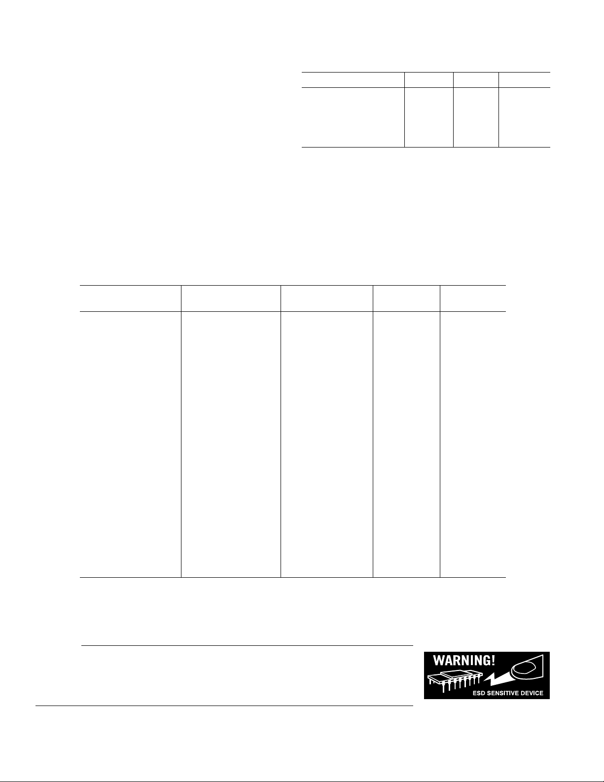
CAUTION
ESD (electrostatic discharge) sensitive device. Electrostatic charges as high as 4000 V readily
accumulate on the human body and test equipment and can discharge without detection. Although the
AD8601/AD8602/AD8604 features proprietary ESD protection circuitry, permanent damage may
occur on devices subjected to high energy electrostatic discharges. Therefore, proper ESD precautions
are recommended to avoid performance degradation or loss of functionality.
REV. D–4–

3,000
TCVOS – V/ⴗC
60
30
0
0101
QUANTITY – Amplifiers
23456789
50
40
20
10
VS = 5V
T
A
= 25ⴗC TO 85ⴗC
VS = 3V
= 25ⴗC
T
A
2,500
2,000
1,500
1,000
QUANTITY – Amplifiers
500
= 0V TO 3V
V
CM
Typical Performance Characteristics–
AD8601/AD8602/AD8604
0
ⴚ1.0
ⴚ0.6 ⴚ0.4 ⴚ0.2
ⴚ0.8
INPUT OFFSET VOLTAGE – mV
0
0.2 0.4 0.6 0.8
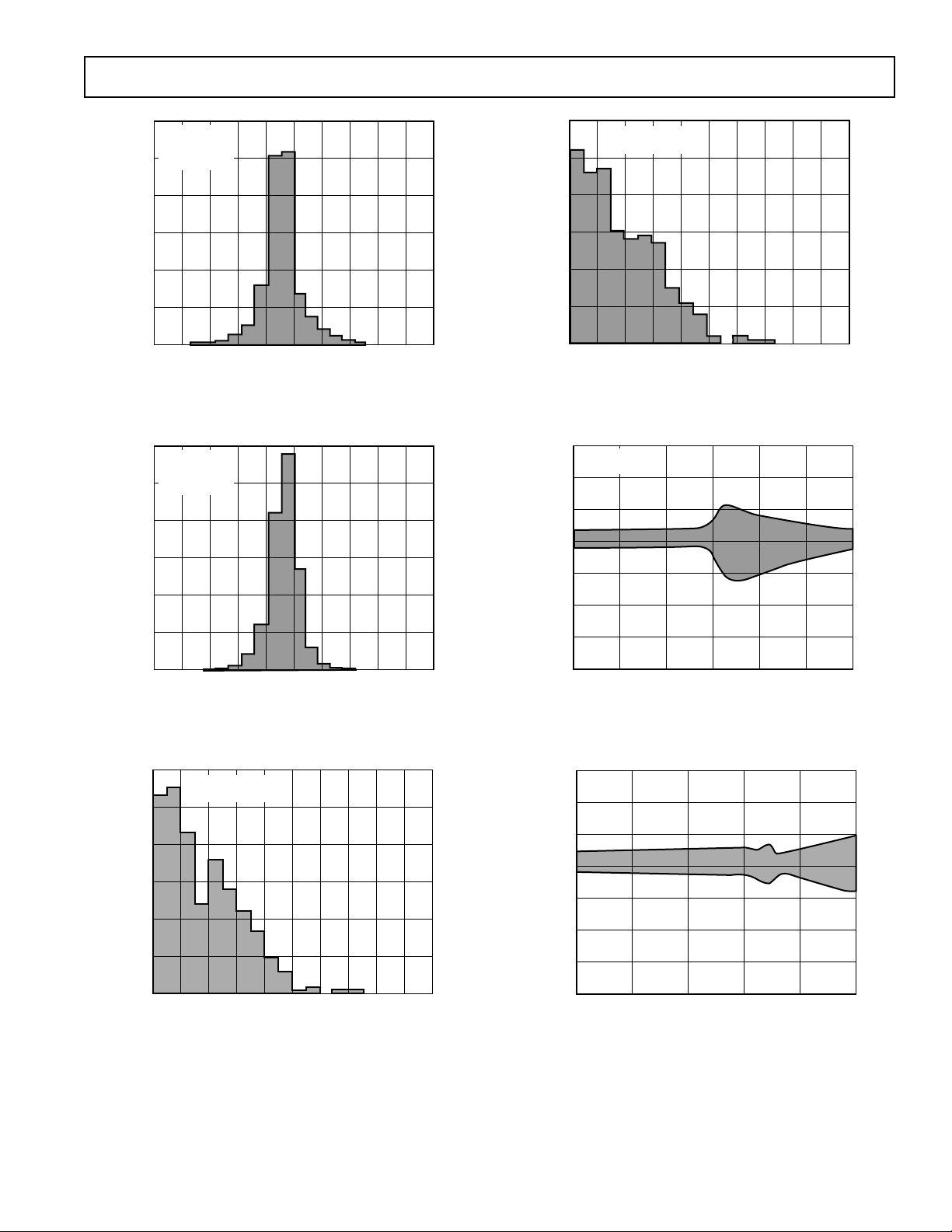
TPC 1. Input Offset Voltage Distribution
3,000
VS = 5V
= 25ⴗC
T
A
2,500
2,000
1,500
1,000
QUANTITY – Amplifiers
500
0
ⴚ1.0
= 0V TO 5V
V
CM
ⴚ0.8
ⴚ0.6 ⴚ0.4 ⴚ0.2
INPUT OFFSET VOLTAGE – mV
0
0.2 0.4 0.6 0.8
TPC 2. Input Offset Voltage Distribution
60
50
VS = 3V
TA = 25ⴗC TO 85ⴗC
1.0
1.0
TPC 4. Input Offset Voltage Drift Distribution
1.5
VS = 3V
= 25ⴗC
T
0
03.00.5
A
1.0 1.5 2.0 2.5
COMMON-MODE VOLTAGE – V
1.0
0.5
ⴚ0.5
ⴚ1.0
INPUT OFFSET VOLTAGE – mV
ⴚ1.5
ⴚ2.0
TPC 5. Input Offset Voltage vs. Common-Mode Voltage
1.5
VS = 5V
= 25ⴗC
T
A
1.0
REV. D
40
30
20
QUANTITY – Amplifiers
10
0
0101
23456789
TCVOS – V/ⴗC
TPC 3. Input Offset Voltage Drift Distribution
0.5
0
ⴚ0.5
ⴚ1.0
INPUT OFFSET VOLTAGE – mV
ⴚ1.5
ⴚ2.0
01
2345
COMMON-MODE VOLTAGE – V
TPC 6. Input Offset Voltage vs. Common-Mode Voltage
–5–

AD8601/AD8602/AD8604
300
VS = 3V
250
200
150
100
INPUT BIAS CURRENT – pA
50
0
ⴚ40
ⴚ25 ⴚ10
535508095110
TEMPERATURE – ⴗC
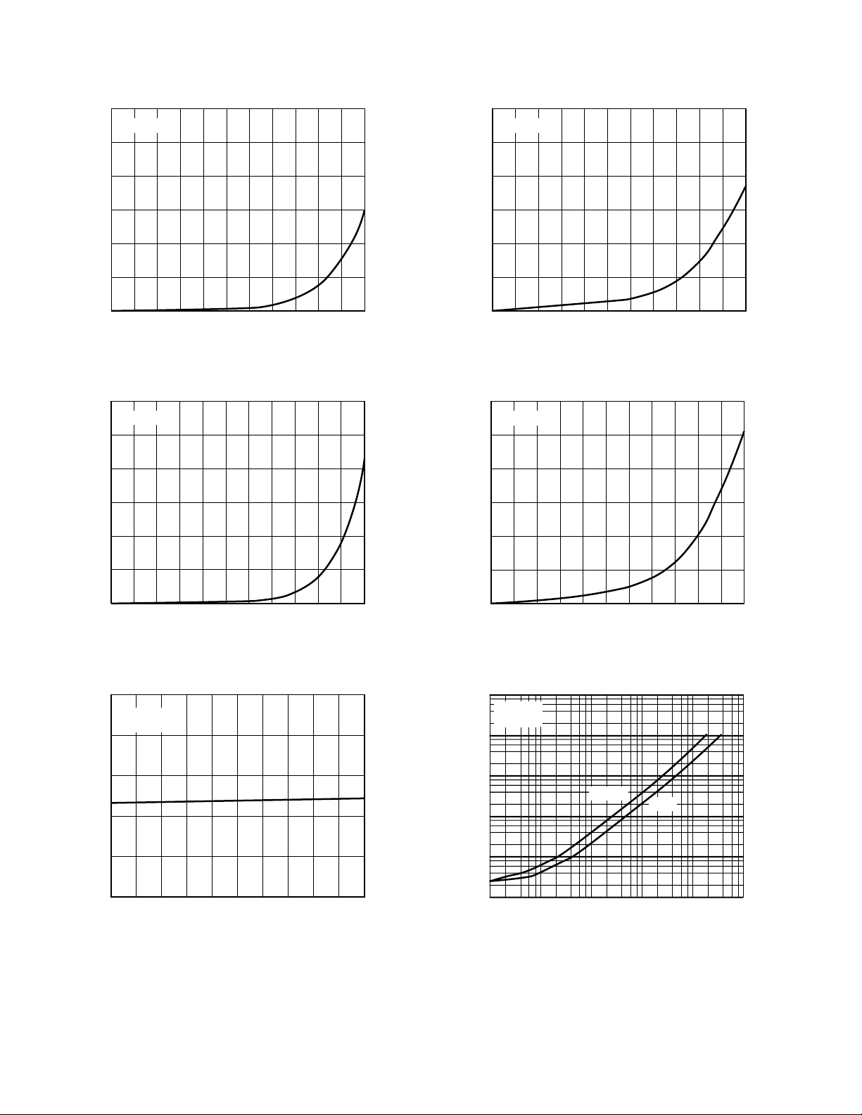
TPC 7. Input Bias Current vs. Temperature
300
VS = 5V
250
200
150
30
VS = 3V
25
20
15
10
INPUT OFFSET CURRENT – pA
5
0
ⴚ40
12520 65
ⴚ25 ⴚ10
535508095110
TEMPERATURE – ⴗC
12520 65
TPC 10. Input Offset Current vs. Temperature
30
VS = 5V
25
20
15
100
INPUT BIAS CURRENT – pA
50
0
ⴚ40
ⴚ25 ⴚ10
535508095110
TEMPERATURE – ⴗC
12520 65
TPC 8. Input Bias Current vs. Temperature
5
VS = 5V
= 25ⴗC
T
A
4
3
2
INPUT BIAS CURRENT – pA
1
0
0 0.5 1.0 1.5 4.5 5.0
2.0 2.5 3.0 3.5
COMMON-MODE VOLTAGE – V
4.0
TPC 9. Input Bias Current vs. Common-Mode Voltage
10
INPUT OFFSET CURRENT – pA
5
0
ⴚ40
ⴚ25 ⴚ10
535508095110
TEMPERATURE – ⴗC
12520 65
TPC 11. Input Offset Current vs. Temperature
10k
VS = 2.7V
T
= 25ⴗC
A
1k
100
10
OUTPUT VOLTAGE – mV
1
0.1
0.001 1000.01
SOURCE
0.1 1 10
LOAD CURRENT – mA
SINK
TPC 12. Output Voltage to Supply Rail vs. Load Current
REV. D–6–
 Loading...