Analog Devices AD8600CHIPS, AD8600AP Datasheet
16-Channel, 8-Bit
a
FEATURES
16 Independently Addressable Voltage Outputs
Full-Scale Set by External Reference
2 µs Settling Time
Double Buffered 8-Bit Parallel Input
High Speed Data Load Rate
Data Readback
Operates from Single +5 V
Optional ±6 V Supply Extends Output Range
APPLICATIONS
Phased Array Ultrasound & Sonar
Power Level Setting
Receiver Gain Setting
Automatic Test Equipment
LCD Clock Level Setting
GENERAL DESCRIPTION
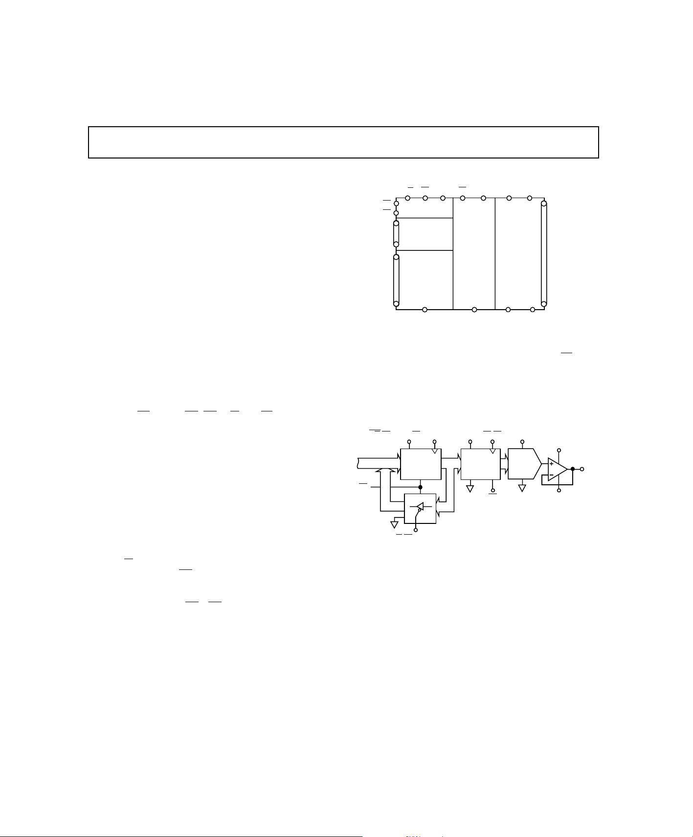
The AD8600 contains 16 independent voltage output digital-toanalog converters that share a common external reference input
voltage. Each DAC has its own DAC register and input register
to allow double buffering. An 8-bit parallel data input, four address pins, a
digital interface.
The AD8600 is constructed in a monolithic CBCMOS process
which optimizes use of CMOS for logic and bipolar for speed
and precision. The digital-to-analog converter design uses voltage mode operation ideally suited to single supply operation.
The internal DAC voltage range is fixed at DACGND to V
The voltage buffers provide an output voltage range that approaches ground and extends to 1.0 V below V
reference voltage values and digital inputs will settle within
±1 LSB in 2 µs.
Data is preloaded into the input registers one at a time after the
internal address decoder selects the input register. In the write
mode (R/
the positive edge of the
be used to load the data. After changes have been submitted to
the input registers, the DAC registers are simultaneously updated by a common load
put voltages simultaneously appear on all 16 outputs.
CS select, a LD, EN, R/W, and RS provide the
.
REF
. Changes in
CC
W low) data is latched into the input register during
EN pulse. Pulses as short as 40 ns can
EN × LD strobe. The new analog out-
Multiplying DAC
AD8600*
FUNCTIONAL BLOCK DIAGRAM
V
RS
DB7
DB6
DB5
DB4
DB3
DB2
DB1
DB0
CS
EN
A3
A2
A1
A0
R/W
CONTROL
ADDRESS
REGISTERS
LOGIC
DECODE
16 x 8
INPUT
D
GND1
DD1
At system power up or during fault recovery the reset (RS) pin
forces all DAC registers into the zero state which places zero
volts at all DAC outputs.
The AD8600 is offered in the PLCC-44 package. The device is
designed and tested for operation over the extended industrial
temperature range of –40°C to +85°C.
R/
W•CS•ADDR•EN
DB7...DB0
RS
D
GND1
R/W•CS•ADDRESS
V
INPUT
REGISTER
DD1
Figure 1. Equivalent DAC Channel
V
LD
DD2VREFVCC
16 x 8
DAC
REGISTERS
AD8600
D
GND2
V
DD2
DAC
REGISTER
D
GND2
LD•EN
RS
8-BIT
DAC
DACGND
DACGND
16
V
REF
R-2R
DAC
O0
O1
O2
O3
O4
O5
O6
O7
O8
S
O9
O10
O11
O12
O13
O14
O15
V
EE
V
CC
O
X
V
EE
*Patent pending.
REV. 0
Information furnished by Analog Devices is believed to be accurate and
reliable. However, no responsibility is assumed by Analog Devices for its
use, nor for any infringements of patents or other rights of third parties
which may result from its use. No license is granted by implication or
otherwise under any patent or patent rights of Analog Devices.
One Technology Way, P.O. Box 9106, Norwood. MA 02062-9106, U.S.A.
Tel: 617/329-4700 Fax: 617/326-8703

AD8600–SPECIFICATIONS
(@ V
= V
SINGLE SUPPLY
DD1
= VCC = +5 V ± 5%, V
DD2
Parameter Symbol Condition Min Typ Max Units
STATIC PERFORMANCE
Resolution N 8 Bits
Relative Accuracy
2
Differential Nonlinearity
Full-Scale Voltage V
Full-Scale Tempco TCV
Zero Scale Error V
Reference Input Resistance R
ANALOG OUTPUT
Output Voltage Range
Output Current I
Capacitive Load C
1
2
2
INL –1 ±1/2 +1 LSB
DNL Guaranteed Monotonic –1 ±1/4 +1 LSB
FS
ZSE
V
ZSE
REF
OVR
OUT
L
Data = FF
Data = FF
FS
Data = 00H, RS = “0,” TA= +25°C +3.5 LSB
Data = 00H, RS = “0” +5 LSB
Data = AB
V
SS
= +2.5 V 0.000 2.500 V
REF
Data = 80
No Oscillation 50 pF
LOGIC INPUTS
Logic Input Low Voltage V
Logic Input High Voltage V
Logic Input Current I
Logic Input Capacitance
3
IL
IH
IL
C
IL
LOGIC OUTPUTS
Logic Out High Voltage V
Logic Out Low Voltage V
AC CHARACTERISTICS
3
Slew Rate SR For ∆V
Voltage Output Settling Time
Voltage Output Settling Time2t
OH
OL
2
t
S1
S2
IOH = –0.4 mA 3.5 V
IOL = 1.6 mA 0.4 V
REF
±1 LSB of Final Value, Full-Scale Data Change 2 µs
±1 LSB of Final Value, ∆V
POWER SUPPLIES
V
Positive Supply Current I
Logic Supply Currents I
Power Dissipation P
CC
DD1&2
DISS
= 5 V, VIL = 0 V, No Load 24 35 mA
IH
V
= 5 V, VIL = 0 V, No Load 0.1 mA
IH
V
= 5 V, VIL = 0 V, No Load 120 175 mW
IH
Power Supply Sensitivity PSS ∆VCC = ±5% 0.007 %/%
Logic Power Supply Range V
Positive Power Supply Range3V
NOTES
1
When V
2
Single supply operation does not include the final 2 LSBs near analog ground. If this performance is critical, use a negative supply (VEE) pin of at least –0.7 V to
–5.25 V. Note that for the INL measurement zero-scale voltage is extrapolated using codes 7
3
Guaranteed by design not subject to production test.
Specifications subject to change without notice.
= 2.500 V, 1 LSB = 9.76 mV.
REF
DDR
CCR
= 0 V, V
EE
H
H
H
H
= +2.500 V, –40°C ≤ TA ≤ +85°C, unless otherwise noted)
REF
2.480 2.490 2.500 V
±20 ppm/°C
1.2 2 kΩ
±2mA
0.8 V
2.4 V
10 µA
10 pF
or FS Code Change 4 7 V/µs
= 1 V, Data = FF
REF
H
2 µs
4.75 5.25 V
to 8010.
10
V
DD
7.0 V
–2–
REV. 0

AD8600
(@ V
= V
DUAL SUPPLY
DD1
= VCC = +5 V ± 5%, V
DD2
Parameter Symbol Condition Min Typ Max Units
STATIC PERFORMANCE
1
Resolution N 8 Bits
Total Unadjusted Error TUE All Other DACs Loaded with Data = 55
Relative Accuracy INL –1 ±1/2 +1 LSB
Differential Nonlinearity DNL Guaranteed Monotonic –1 ±1/4 +1 LSB
Full-Scale Voltage V
Full-Scale Voltage Error V
FS
FSE
Full-Scale Tempco TCV
Zero Scale Error V
Zero Scale Error V
Zero Scale Error V
ZSE
ZSE
ZSE
Zero Scale Tempco TCV
Reference Input Resistance R
Reference Input Capacitance2C
REF
REF
Data = FFH, V
Data = FFH, V
Data = FFH, V
FS
Data = 00H, RS = “0,” TA = +25°C–2±1+2 mV
Data = 00H, All Other DACs Data = 00
Data = 00H, All Other DACs Data = 55
Data = 00H, VCC = +5 V, VEE = –5 V ±10 µV/°C
ZS
Data = AB
Data = AB
ANALOG OUTPUT
V
Output Voltage Range OVR
Output Voltage Range
Output Current I
Capacitive Load
2
2
OVR
OUT
C
L
1
2
= +3.5 V 0.000 3.500 V
REF
V
= V
CC
Data = 80
No Oscillation 50 pF
LOGIC INPUTS
Logic Input Low Voltage V
Logic Input High Voltage V
Logic Input Current I
Logic Input Capacitance
2
IL
IH
IL
C
IL
LOGIC OUTPUTS
Logic Out High Voltage V
Logic Out Low Voltage V
AC CHARACTERISTICS
2
OH
OL
IOH = –0.4 mA 3.5 V
IOL = 1.6 mA 0.4 V
Reference In Bandwidth BW –3 dB Frequency, V
Slew Rate SR For ∆ V
Voltage Noise Density e
Digital Feedthrough FT Digital Inputs to DAC Outputs 10 nVs
Voltage Output Settling Time
Voltage Output Settling Time3t
N
3
t
S1
S2
f = 1 kHz, V
±1 LSB of Final Value, FS Data Change 1 2 µs
±1 LSB of Final Value, ∆V
POWER SUPPLIES
V
Positive Supply Current I
Negative Supply Current I
Logic Supply Currents I
Power Dissipation
4
CC
EE
DD1&2
P
DISS
= 5 V, VIL = 0 V, VEE = –5 V, No Load 22 35 mA
IH
V
= 5 V, VIL = 0 V, VEE = –5 V, No Load 22 35 mA
IH
V
= 5 V, VIL = 0 V, VEE = –5 V, No Load 0.1 mA
IH
V
= 5 V, VIL = 0 V, VEE = –5 V, No Load 225 350 mW
IH
Power Supply Sensitivity PSS ∆ VCC & ∆VEE = ±5% 0.007 %/%
Logic Power Supply Range V
Pos Power Supply Range
Neg Power Supply Range
NOTES
1
When V
2
Guaranteed by design not subject to production test.
3
Settling time test is performed using RL = 50 kΩ and CL = 35 pF.
4
Power Dissipation is calculated using 5 V × (IDD + |ISS| + I
Specifications subject to change without notice.
= +3.500 V, 1 LSB = 13.67 mV.
REF
2
2
V
V
DDR
CCR
EER
DD1
= –5 V ± 5%, V
EE
REF
REF
REF
H
H
= +7 V, V
DD2
H
= +3.5 V 3.473 3.486 3.500 V
= +3.5 V –1 +1 LSB
= +3.5 V ±20 ppm/°C
EE
= +3.500 V, –40°C ≤ TA ≤ +85°C, unless otherwise noted)
REF
H
H
H
–1 ±3/4 +1 LSB
–1 +1 LSB
±1/2 LSB
1.2 2 kΩ
= –0.7 V, V
= 5 V 0.000 5.000 V
REF
±2mA
240 pF
0.8 V
2.4 V
10 µA
10 pF
= 2.5 VDC + 0.1 V
or FS Code Change 4 7 V/µs
REF
REF
= 0 V 46 nV/√Hz
REF
= 1 V, Data = FF
REF
AC
500 kHz
H
12 µs
4.75 5.25 V
V
DD
7.0 V
–5.25 0.0 V
+ I
).
DD2
REV. 0
–3–
AD8600
(@ V
= V
= VCC = +5 V ± 5%, V
DD2
ELECTRICAL CHARACTERISTICS
DD1
unless otherwise noted)
Parameter Symbol Condition Min Typ Max Units
INTERFACE TIMING
Clock (EN) Frequency f
EN) High Pulse Width t
Clock (
EN) LowPulse Width t
Clock (
Data Setup Time t
Data Hold Time t
Address Setup Time t
Address Hold Time t
Valid Address to Data Valid t
Load Enable Setup Time t
Load Enable Hold Time t
Read/Write to Clock (
Read/Write to DataBus Hi-Z t
Read/Write to DataBus Active t
EN) to Read/Write t
Clock (
EN) to Chip Select t
Clock (
Chip Select to Clock (
Chip Select to Data Valid t
Chip Select to DataBus Hi-Z t
Reset Pulse Width t
NOTES
1
Guaranteed by design not subject to production test.
2
All logic input signals have maximum rise and fall times of 2 ns.
Specifications subject to change without notice.
1, 2
CLK
CH
CL
DS
DH
AS
AH
AD
LS
EN)t
EN)t
LH
RWC
RWZ
RWD
TWH
TCH
CSC
CSD
CSZ
RS
Data Loading 12.5 MHz
= –5 V, V
EE
= +3.500 V, –40°C ≤ TA ≤ +85°C,
REF
40 ns
40 ns
40 ns
10 ns
0ns
0ns
160 ns
0ns
0ns
30 ns
120 ns
120 ns
0ns
0ns
30 ns
120 ns
150 ns
25 ns
R/W
DATA
ADDR
EN
CS
t
RWZ
t
t
RWC
AS
t
DS
t
CSC
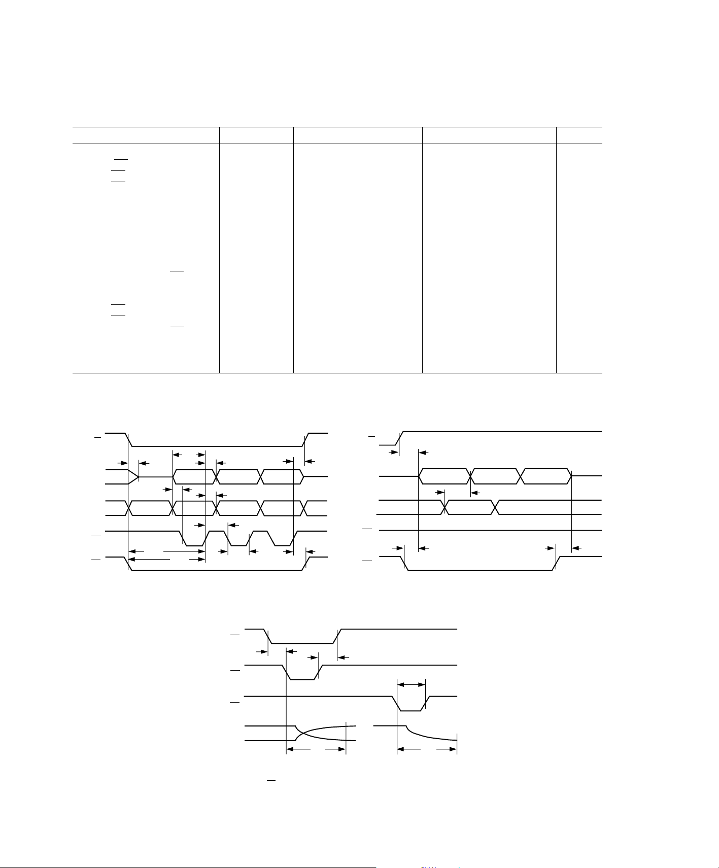
Figure 2. Write Timing
R/W
t
TWH
t
DH
t
AH
t
CH
t
CL
t
TCH
HIGH-Z
DATA
ADDR
EN
CS
HIGH -Z
t
t
RWD
CSD
t
AD
t
CSZ
Figure 3. Readback Timing
LD
t
LS
EN
RS
OUT
t
LH
t
RS
t
S1
t
S1
Figure 4. Write to DAC Register & Voltage Output Settling
Timing (CS= High, Prevents Input Register Changes)
–4–
REV. 0
AD8600
ABSOLUTE MAXIMUM RATINGS
(TA= +25°C unless otherwise noted)
V
(Digital Supply) to GND . . . . . . . . . . . . . .–0.3 V, +7 V
DD1
(DAC Buffer/Driver Supply) . . . . . . . . . . . . –0.3 V, +7 V
V
DD2
(Analog Supply) to GND . . . . . . . . . . . . . . . –0.3 V, +7 V
V
CC
(Analog Supply) to GND . . . . . . . . . . . . . . . +0.3 V, –7 V
V
EE
to GND . . . . . . . . . . . . . . . . . . . . . . –0.3 V, V
V
REF
to V
V
DD2
to GND . . . . . . . . . . . . . . . . . . . . . . . . . . . . . . . . . V
V
OUT
Short Circuit Duration
V
OUT
. . . . . . . . . . . . . . . . . . . . . . . . . . . . . . . . .–0.3 V
REF
to GND or Power Supplies
1
. . . . . . . . . . . . . . .
Digital Input/Output Voltage to GND . . . –0.3 V, V
Thermal Resistance–Theta Junction-to-Ambient (θ
+ 0.3 V
CC
CC
Continuous
+ 0.3 V
DD
)
JA
PLCC-44 . . . . . . . . . . . . . . . . . . . . . . . . . . . . . . . . 47°C/W
– T
Package Power Dissipation . . . . . . . . . . . . . . . . (T
Maximum Junction Temperature T
max . . . . . . . . . . . 150°C
J
)/θ
J
A
JA
Operating Temperature Range . . . . . . . . . . . . –40°C to +85°C
Storage Temperature Range . . . . . . . . . . . . –65°C to +150°C
Lead Temperature (Soldering, 10 sec) . . . . . . . . . . . . +300°C
NOTE
1
No more than four outputs may be shorted to power or GND simultaneously.
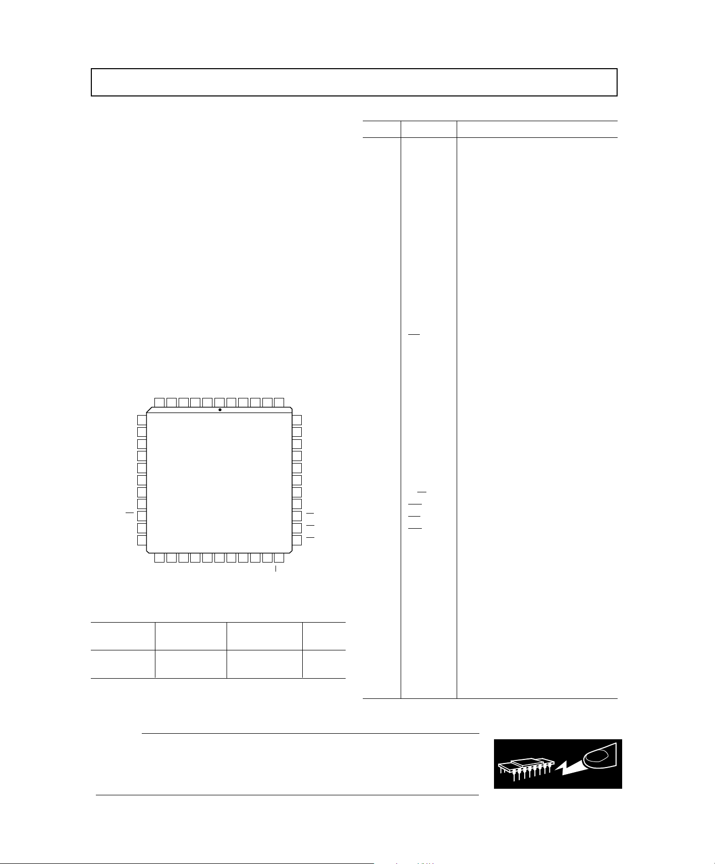
PIN CONFIGURATION
CC
DD2
DGND2
V
V
43
25 28
26
A2
A0
A1
EE
V
O8
404142
O9
39
38
O10
O11
37
O12
36
35
O13
34
O14
33
O15
32
DGND1
31
LD
30
CS
29
EN
27
A3
R/W
O6
7
8
O5
9
O4
10
O3
O2
11
O1
12
13
O0
V
14
DD1
RS
15
DB0
16
DB1
17
NC = NO CONNECT
O7
DB2
EE
V
DB3
CC
V
DB4
REF
NC
DACGND
V
3
AD8600
TOP VIEW
(Not to Scale)
21 24
22182019
23
DB7
DB5
DB6
4412645
ORDERING GUIDE
Package Package
Model Temperature Description Option
AD8600AP –40°C to +85°C 44-Lead PLCC P-44A
AD8600Chips +25°C Die*
*For die specifications contact your local Analog Devices sales office.
The AD8600 contains 5782 transistors.
PIN DESCRIPTION
Pin No. Name Description
1 NC No Connection
2V
REF
Reference input voltage common
to all DACs.
3 DACGND DAC Analog Ground Return. Sets
analog zero-scale voltage.
4V
5V
CC
EE
Output Amplifier Positive Supply
Output Amplifier Negative Supply
6 O7 DAC Channel Output No. 7
7 O6 DAC Channel Output No. 6
8 O5 DAC Channel Output No. 5
9 O4 DAC Channel Output No. 4
10 O3 DAC Channel Output No. 3
11 O2 DAC Channel Output No. 2
12 O1 DAC Channel Output No. 1
13 O0 DAC Channel Output No. 0
14 V
15
DD1
RS Active Low Reset Input Pin
Digital Logic Power Supply
16 DB0 Data Bit Zero I/O (LSB)
17 DB1 Data Bit I/O
18 DB2 Data Bit I/O
19 DB3 Data Bit I/O
20 DB4 Data Bit I/O
21 DB5 Data Bit I/O
22 DB6 Data Bit I/O
23 DB7 Most Significant Data Bit I/O (MSB)
24 A0 Address Bit Zero (LSB)
25 A1 Address Bit
26 A2 Address Bit
27 A3 Most Significant Addr Bit (MSB)
28 R/
29
30
31
W Read/Write Select Control Input
EN Active Low Enable Clock Strobe
CS Chip Select Input
LD DAC Register Load Strobe
32 DGND1 Digital Ground Input No. 1
33 O15 DAC Channel Output No. 15
34 O14 DAC Channel Output No. 14
35 O13 DAC Channel Output No. 13
36 O12 DAC Channel Output No. 12
37 O11 DAC Channel Output No. 11
38 O10 DAC Channel Output No. 10
39 O9 DAC Channel Output No. 9
40 O8 DAC Channel Output No. 8
41 V
42 V
EE
CC
Output Amplifier Negative Supply
Output Amplifier Positive Supply
43 DGND2 Digital Ground Input No. 2
44 V
DD2
DAC Analog Supply Voltage
CAUTION
ESD (electrostatic discharge) sensitive device. Electrostatic charges as high as 4000 V readily
accumulate on the human body and test equipment and can discharge without detection.
Although the AD8600 features proprietary ESD protection circuitry, permanent damage may
occur on devices subjected to high energy electrostatic discharges. Therefore, proper ESD
precautions are recommended to avoid performance degradation or loss of functionality.
REV. 0
–5–
WARNING!
ESD SENSITIVE DEVICE
 Loading...