

Page 1
Dual, Ultralow Distortion,
FEATURES
Low noise: 1 nV/√Hz at 1 kHz
Low distortion: −105 dB THD @ 20 kHz
<80 nV p-p input noise, 0.1 Hz to 10 Hz
Slew rate: 16 V/μs
Wide bandwidth: 10 MHz
Supply current: 4.7 mA/amp typical
Low offset voltage: 10 μV typical
CMRR: 120 dB
Unity-gain stable
±15 V operation
APPLICATIONS
Professional audio preamplifiers
ATE/precision testers
Imaging systems
Medical/physiological measurements
Precision detectors/instruments
Precision data conversion
Ultralow Noise Op Amp
AD8599
PIN CONFIGURATION
1
OUT A
–IN A
+IN A
AD8599
2
3
TOP VIEW
(Not to S cale)
–V
4
Figure 1. 8-Lead SOIC (R-8)
8
7
6
5
+V
OUT B
–IN B
+IN B
06274-054
GENERAL DESCRIPTION
The AD8599 is a dual, very low noise, low distortion operational amplifier ideal for use as a preamplifier. The low noise of
1 nV/√Hz and low harmonic distortion of −105 dB (or better)
at audio bandwidths give the AD8599 the wide dynamic range
necessary for preamps in audio, medical, and instrumentation
applications. The AD8599’s excellent slew rate of 16 V/μs and
10 MHz gain bandwidth make it highly suitable for medical
applications. The low distortion and settling time of the AD8599
make it ideal for buffering of high resolution data converters.
The AD8599 is available in an 8-Lead SOIC package and is
specified over a −40°C to +125°C temperature range.
Rev. A
Information furnished by Analog Devices is believed to be accurate and reliable. However, no
responsibility is assumed by Anal og Devices for its use, nor for any infringements of patents or ot her
rights of third parties that may result from its use. Specifications subject to change without notice. No
license is granted by implication or otherwise under any patent or patent rights of Analog Devices.
Trademarks and registered trademarks are the property of their respective owners.
One Technology Way, P.O. Box 9106, Norwood, MA 02062-9106, U.S.A.
Tel: 781.329.4700 www.analog.com
Fax: 781.461.3113 ©2007 Analog Devices, Inc. All rights reserved.
Page 2

AD8599
TABLE OF CONTENTS
Features.............................................................................................. 1
Applications....................................................................................... 1
Pin Configuration............................................................................. 1
General Description......................................................................... 1
Revision History ...............................................................................2
Specifications..................................................................................... 3
Absolute Maximum Ratings............................................................ 4
REVISION HISTORY
4/07—Rev. 0 to Rev. A
Updated Layout................................................................................. 5
Changes to Figure 45 Caption....................................................... 12
Added Figure 48.............................................................................. 12
Changes to Figure 51 Caption....................................................... 13
2/07—Revision 0: Initial Version
Thermal Resistance.......................................................................4
Power Sequencing.........................................................................4
ESD Caution...................................................................................4
Typical Performance Characteristics..............................................5
Outline Dimensions....................................................................... 14
Ordering Guide .......................................................................... 14
Rev. A | Page 2 of 16
Page 3

AD8599
SPECIFICATIONS
VS = ±15 V, VCM = 0 V, VO = 0 V, TA = +25°C, unless otherwise specified.
Table 1.
Parameter Symbol Conditions Min Typ Max Unit
INPUT CHARACTERISTICS
Offset Voltage V
OS
−40°C ≤ TA ≤ +125°C 180 μV
Offset Voltage Drift ΔVOS/ΔT −40°C ≤ TA ≤ +125°C 0.8 2.2 μV/°C
Input Bias Current I
B
−40°C ≤ TA ≤ +125°C 300 nA
Input Offset Current I
OS
−40°C ≤ TA ≤ +125°C 220 nA
Input Voltage Range IVR
Common-Mode Rejection Ratio CMRR −12.5 V ≤ VCM ≤ +12.5 V 120 140 dB
−40°C ≤ TA ≤ +125°C 115 dB
Large Signal Voltage Gain AVO R
−40°C ≤ TA ≤ +125°C 106 dB
Input Capacitance C
C
4.8 pf
DIFF
CM
OUTPUT CHARACTERISTICS
Output Voltage High V
OH
−40°C ≤ TA ≤ +125°C 12.8 V
R
−40°C ≤ TA ≤ +125°C 13.2 V
Output Voltage Low V
OL
−40°C ≤ TA ≤ +125°C −12.8 V
R
−40°C ≤ TA ≤ +125°C −13.3 V
Output Source Circuit I
Closed-Loop Output Impedance Z
SC
At 1 MHz, AV = 1 5 Ω
OUT
POWER SUPPLY
Power Supply Rejection Ratio PSRR VDD = ±18 V to ±4.5 V 120 140 dB
−40°C ≤ TA ≤ +125°C 118 dB
Supply Current per Amplifier ISY 4.7 5.7 mA
−40°C ≤ TA ≤ +125°C 6.75 mA
DYNAMIC PERFORMANCE
Slew Rate SR AV = −1, RL = 2 kΩ 16.8 V/μs
A
Settling Time ts To 0.01%, step = 10 V 2 μs
Gain Bandwidth Product GBP 10 MHz
Phase Margin
φ
M
NOISE PERFORMANCE
Peak-to-Peak Noise en p-p 0.1 Hz to 10 Hz 76 nV
Voltage Noise Density e
n
f = 10 Hz 1.5 nV/√Hz
Current Noise f = 1 kHz 1.5 pA/√Hz
Total Harmonic Distortion + Noise THD + N
Channel Separation CS f = 10 kHz −120 dB
10 120 μV
25 180 nA
25 180 nA
VDD = ±15 V −12.5 +12.5 V
≥ 600 Ω, VO = −11 V to +11 V 110 116 dB
L
4.5 pf
RL = 600 Ω 13.1 13.4 V
= 2 kΩ 13.5 13.7 V
L
RL = 600 Ω −13.2 −12.9 V
= 2 kΩ −13.5 −13.4 V
L
±52 mA
= 1, RL = 2 kΩ 15 V/μs
V
68 Degrees
f = 1 kHz 1.07 1.15 nV/√Hz
G = 1, RL ≥ 1 kΩ, f = 1 kHz, V
G = 1, R
≥ 1 kΩ, f = 20 kHz, V
L
RMS
= 3 V
RMS
= 3 V
−108 dB
−105 dB
Rev. A | Page 3 of 16
Page 4
AD8599
ABSOLUTE MAXIMUM RATINGS
Table 2.
Parameter Rating
Supply Voltage ±18 V
Input Voltage GND to V
Differential Input Voltage ±1 V
Output Short-Circuit to GND Indefinite
Storage Temperature Range −65°C to +150°C
Operating Temperature Range −40°C to +125°C
Lead Temperature Range (Soldering 60 sec) 300°C
Junction Temperature 150°C
Stresses above those listed under Absolute Maximum Ratings
may cause permanent damage to the device. This is a stress
rating only; functional operation of the device at these or any
other conditions above those indicated in the operational
section of this specification is not implied. Exposure to absolute
maximum rating conditions for extended periods may affect
device reliability.
DD
THERMAL RESISTANCE
θJA is specified for the worst-case conditions, that is, a device
soldered in a circuit board for surface-mount packages.
Table 3. Thermal Resistance
Package Type θJA θ
8-Lead SOIC (R-8) 120 36 °C/W
Unit
JC
POWER SEQUENCING
The op amp supplies must be established simultaneously with,
or before, any input signals are applied.
If this is not possible, the input current must be limited to 10 mA.
ESD CAUTION
Rev. A | Page 4 of 16
Page 5
AD8599
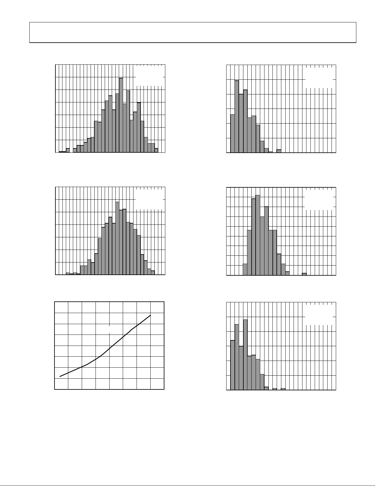
TYPICAL PERFORMANCE CHARACTERISTICS
NUMBER OF AMPLIFIE RS
70
60
50
40
30
20
10
MEAN = 8.23
STDEV = 24.47
MIN = –72.62
MAX = 62.09
NUMBER OF AMPL IFIERS
60
MEAN = 0.346
50
40
30
20
10
STDEV = 0.218
MIN = 0.010
MAX = 1.155
0
–75 –65 –55 –45 –35 –25 –15 –5 15 25 35 45 55 65 755
VOS (µV)
Figure 2. Input Offset Voltage Distribution, V
70
60
50
40
30
20
NUMBER OF AMPL IFIERS
10
0
–75 –65 –55 –45 –35 –25 –15 –5 15 25 35 45 55 65 755
VOS (µV)
Figure 3. Input Offset Voltage Distribution, V
60
50
40
30
VS = ±15V
= ±5 V
S
MEAN = 7.91
STDEV = 21.89
MIN = –63.02
MAX = 57.5
= ±15 V
S
0
06274-001
06274-002
0 0.2 1.6 1.8 2. 0 2.41.41.21.00.4 0.6 0.8 2. 2
Figure 5. TCV
45
40
35
30
25
20
15
NUMBER OF AMPLIFIE RS
10
5
0
0 0.2 1.6 1.8 2. 0 2.41.41.21.00.4 0.6 0.8 2.2
Figure 6. TCV
60
50
40
Distribution, VS = ±5 V, −40°C ≤ TA ≤ +125°C
OS
Distribution, VS = ±15 V, −40°C ≤ TA ≤ +125°C
OS
TCVOS (µV)
TCVOS (µV)
MEAN = 0.765
STDEV = 0.234
MIN = 0.338
MAX = 1.709
MEAN = 0.342
STDEV = 0.221
MIN = 0.013
MAX = 1.239
06274-004
06274-007
(µV)
20
OS
V
10
0
–10
–20
–50 –25 0 25 50 75 100 125 150
TEMPERATURE (° C)
Figure 4. Input Offset Voltage vs. Temperature
06274-003
Rev. A | Page 5 of 16
30
20
NUMBER OF AMPLIFIERS
10
0
0 0.2 1.6 1.8 2. 0 2.41.41.21.00.4 0.6 0.8 2. 2
Figure 7. TCV
Distribution, VS = ±15 V , −40°C ≤ TA ≤ +85°C
OS
TCVOS (µV)
06274-005
Page 6

AD8599
60
MEAN = 0.461
50
40
30
20
NUMBER OF AMPLIFIE RS
10
0
0 0.2 1.6 1.8 2. 0 2.41.41.21.00.4 0.6 0.8 2. 2
Figure 8. TCV
0
–5
–10
(µV)
–15
OS
V
–20
–25
–30
01234
Distribution, VS = ±5 V, −40°C ≤ TA ≤ +85°C
OS
TCVOS (µV)
= ±15V
V
S
VS = ±5V
TIME (Minute)
STDEV = 0.245
MIN = 0.026
MAX = 1.26
06274-006
5
06274-008
100
75
50
25
(µV)
0
OS
V
–25
–50
–75
–100
–15 –10 –5 0 5
VCM (V)
Figure 11. Offset Voltage vs. V
350
300
250
200
150
100
(nA)
B
50
I
0
–50
–100
–150
–200
–50 –25 0 25 50
TEMPERATURE ( °C)
, VS = ±15 V
CM
75 100
10 15
125
06274-010
06274-011
Figure 9. Offset Voltage vs. Time
100
75
50
25
(µV)
0
OS
V
–25
–50
–75
–100
–5.0 –2.5 0 2.5 5.0
VCM (V)
Figure 10. Offset Voltage vs. Common-Mode Voltage, V
= ±5 V
S
Figure 12. Input Bias Current vs. Temperature, V
350
300
250
200
150
100
(nA)
B
50
I
0
–50
–100
–150
–200
–50 –25 0 25 50
06274-009
TEMPERATURE ( °C)
Figure 13. Input Bias Current vs. Temperature, V
= ±5 V, VCM = 0 V
S
75 100
= ±15 V, VCM = 0 V
S
125
06274-012
Rev. A | Page 6 of 16
Page 7

AD8599
80
70
60
50
40
(nA)
OS
I
30
20
10
–50 –25 0 25 50
IOS @ VS = ±5V
IOS @ VS = ±15V
75 1000125
TEMPERATURE ( °C)
Figure 14. Input Offset Current vs. Temperature
350
300
250
200
150
100
50
0
(nA)
B
I
–50
–100
–150
–200
–250
–300
–350
–12 –10 –8 –6 –4
TA = –40°C
TA = +25°C
TA = +85°C
TA = +125°C
–2 0
VCM (V)
42
Figure 15. Input Bias Current vs. Voltage Common Mode; V
120
118
116
(dB)
VO
A
114
112
110
06274-013
–50 –25 0 25 50
RL = 600Ω, VO = ±11V
Figure 17. Large Signal Voltage Gain vs. Temperature, V
80
60
I
40
20
0
–20
OUTPUT CURRENT (mA)
–40
–60
6
12
108
= ±15 V
S
06274-014
–80
–50 –25 0 25 50
Figure 18. Output Current vs. Temperature, V
SINK
I
SOURCE
RL = 2kΩ, VO = ±11V
75 100
TEMPERATURE (° C)
75 100
TEMPERATURE (° C)
= ±5 V
S
150125
= ±15 V
S
150125
06274-016
06274-017
114
112
110
108
(dB)
VO
106
A
104
102
100
RL = 600Ω, VO = ±2V
RL = 2kΩ, VO = ±2V
75 100
TEMPERATURE (° C)
Figure 16. Large Signal Voltage Gain vs. Temperature, V
= ±5 V
S
150125–50 –25 0 25 50
06274-015
Rev. A | Page 7 of 16
80
60
I
40
20
0
–20
OUTPUT CURRENT (mA)
–40
–60
–80
–50 –25 0 25 50
SINK
I
SOURCE
TEMPERATURE (° C)
Figure 19. Output Current vs. Temperature, V
75 100
= ±15 V
S
150125
06274-018
Page 8

AD8599
14
10000
12
10
8
(mA)
SY
6
I
4
2
0
0481216
ISY = +125°C
Figure 20. Supply Current vs. Supply Voltage
15.0
12.5
10.0
(mA)
SY
I
7.5
ISY ±15V
ISY ±5V
20 24
VSY (V)
ISY = +85°C
ISY = +25°C
ISY = –40°C
I
SINK
1000
OUTPUT SAT URATION VO LTAGE (mV)
100
3228
4036
06274-019
0.001 0.01 0. 1 1 10
Figure 23. Output Saturation Voltage vs. Current Load, V
10000
1000
I
SOURCE
IL (mA)
VDD – V
100
06274-022
= ±15 V
S
OH
5.0
TEMPERATURE ( °C)
75 100
Figure 21. Supply Current vs. Temperature
10000
I
SINK
1000
OUTPUT SAT URATION VO LTAGE (mV)
100
0.001 0.01 0.1 1 10
I
SOURCE
IL (mA)
Figure 22. Output Saturation Voltage vs. Current Load, V
125–50 –25 0 25 50
100
= ±5 V
S
OUTPUT SATURAT ION VOL TAGE (mV)
100
06274-020
100 1000 10000 100000 1000000
Figure 24. Output Saturation Voltage vs. R
10000
1000
OUTPUT SATURAT ION VOL TAGE (mV)
100
06274-021
100 1000 10000 100000 1000000
Figure 25. Output Saturation Voltage vs. R
OUTPUT LOAD (Ω)
VEE – V
OL
OUTPUT LOAD (Ω)
, VS = ±5 V
L
, VS = ±5 V
L
06274-023
06274-024
Rev. A | Page 8 of 16
Page 9

AD8599
V
V
V
V
10000
0
–0.5
VDD – V
OH
1000
OUTPUT SATURATION VOLTAGE (mV)
100
100 1000 10000 100000 1000000
Figure 26. Output Saturation Voltage vs. R
10000
1000
OUTPUT SATURATION VOL TAGE (mV)
100
100 1000 10000 100000 1000000
Figure 27. Output Saturation Voltage vs. R
2.5
OUTPUT LOAD (Ω)
VEE – V
OL
OUTPUT LOAD (Ω)
, VS = ±15 V
L
, VS = ±15 V
L
–1.0
(V)
OL
–
EE
–1.5
V
–2.0
–2.5
06274-025
–50 –25 0 25 50
Figure 29. Output Saturation Voltage vs. Temperature, V
2.5
2.0
1.5
(V)
OH
–
CC
1.0
V
0.5
0
06274-026
–50 –25 0 25 50
Figure 30. Output Saturation Voltage vs. Temperature, V
0
VEE – VOL@ RL = 2kΩ
VEE – VOL@ RL = 600Ω
TEMPE RATURE ( °C)
VCC – VOH@ RL = 600Ω
VCC – VOH@ RL = 2kΩ
TEMPERATURE ( °C)
75 100 125 150
= ±5 V
S
75 100 125 150
= ±15 V
S
06274-028
06274-029
2.0
1.5
(V)
OH
–
CC
1.0
V
0.5
0
–50 –25 0 25 50
VCC – VOH@ RL = 600Ω
VCC – VOH@ RL = 2kΩ
75 100 125 150
TEMPERATURE (° C)
Figure 28. Output Saturation Voltage vs. Temperature, V
= ±5 V
S
06274-027
Rev. A | Page 9 of 16
–0.5
–1.0
(V)
OL
–
EE
–1.5
V
–2.0
–2.5
–50 –25 0 25 50
VEE – VOL@ RL = 2kΩ
VEE – VOL@ RL = 600Ω
75 100 125 150
TEMPERATURE (° C)
Figure 31. Output Saturation Voltage vs. Temperature, V
= ±15 V
S
06274-030
Page 10

AD8599
–
15.0
14.8
14.6
14.4
14.2
(V)
14.0
OH
V
13.8
13.6
13.4
13.2
13.0
–50 0 50
VOH@ RL = 600Ω
VOH@ RL = 2kΩ
TEMPE RATURE ( °C)
Figure 32. Output Voltage High vs. Temperature, V
13.0
–13.5
(V)
–14.0
OL
V
–14.5
–15.0
–50 0 50
VOL@ RL = 600Ω
VOL@ RL = 2kΩ
TEMPERATURE ( °C)
Figure 33. Output Voltage Low vs. Temperature, V
30
25
20
15
10
MAXIMUM OUTPUT SWING (V p-p)
VS = ±15V
VS = ±5V
5
100 150
= ±15 V
S
100 150
= ±15 V
S
120
100
80
60
40
GAIN (dB)
20
0
–20
–40
06274-031
1k 10k 100k 1M 10M
GAIN (dB)
PHASE (Degrees)
FREQUENCY (Hz)
Figure 35. Gain and Phase vs. Frequency, ±5 V ≤ V
50
40
30
20
10
0
–10
–20
CLOSED-LOOP GAIN (dB)
–30
–40
–50
06274-032
GAIN = 100
GAIN = 10
GAIN = 1
1k 10k 100k 1M 10M
FREQUENCY (Hz)
Figure 36. Closed-Loop Gain vs. Frequency, ±5 V ≤ V
70
60
GAIN = 100
50
40
(Ω)
OUT
Z
30
20
10
GAIN = 10
GAIN = 1
100M
≤ ±15 V
S
≤ ±15 V
S
120
100
80
60
40
20
0
–20
–40
100M
PHASE (Degrees)
06274-034
06274-035
0
1 10 100 1000 10000
FREQUENCY (kHz)
Figure 34. Maximum Output Swing vs. Frequency
06274-033
0
1k 10k 100k 1M 10M
FREQUENCY (Hz)
Figure 37. Closed-Loop Output Impedance vs. Frequency, ±5 V ≤ V
100M
≤ ±15 V
S
06274-036
Rev. A | Page 10 of 16
Page 11

AD8599
140
120
100
80
60
CMRR (dB)
40
20
0
10 100 1k 10k 100k
FREQUENCY (Hz)
CMRR –VS = ±5V (dB)
CMRR –V
= ±15V (dB)
S
1M
Figure 38. Common-Mode Rejection Ratio vs. Frequency
120
100
80
60
40
PSRR (dB)
20
PSRR+ (dB)
PSRR– (dB)
10M 100M
06274-037
600
500
400
300
200
NUMBER OF AMPLI FIERS
100
0
0.95 0.98 1.01 1.04 1.07 1.10 1. 13 1. 16 1.19
VOLTAGE NOISE DENSITY (nV / Hz)
Figure 41. Voltage Noise Density @ 1 kHz, ±5 V ≤ V
100
10
1
MEAN = 1.07
STDEV = 0.02
MIN = 1.05
MAX = 1.15
≤ ±15 V
S
06274-040
0
–20
100 1k 10k 100k 1M
FREQUENCY (Hz)
Figure 39. Power Supply Rejection Ratio vs. Frequency, ±5 V ≤ V
90
80
70
60
50
40
30
NUMBER OF AMPLIFIERS
20
10
0
1.0 1.1 1.2 1. 3 1.4 1. 5 1.6 1.7 1. 9 2.01.8
VOLTAGE NOISE DENSI TY (nV/ Hz)
Figure 40. Voltage Noise Density @ 10 kHz, ±5 V ≤ V
MEAN = 1.30
STDEV = 0.09
MIN = 1.1
MAX = 1.5
≤ ±15 V
S
10M
≤ ±15 V
S
VOLTAGE NO ISE DENSIT Y (nV/ Hz)
0.1
06274-038
1 10 100 1000
Figure 42. Voltage Noise Density vs. Frequency, ±5 V ≤ V
100
10
1
CURRTENT NOISE DENSITY (pA/ Hz)
0.1
06274-039
1 10 100 1000
FREQUENCY (Hz)
FREQUENCY (Hz)
≤ ±15 V
S
06274-041
06274-042
Figure 43. Current Noise Density vs. Frequency, ±5 V ≤ VS ≤ ±15 V
Rev. A | Page 11 of 16
Page 12

AD8599
0.1
0.01
20
15
10
5
THD + N (%)
0.001
0.0001
10 100 1000 10000 100000
FREQUENCY (Hz)
RL = 600Ω
RL = 2kΩ
Figure 44. Total Harmonic Distortion + Noise vs. Frequency, V
= 3 V rms
V
IN
0.1
VIN = 3V rms
= 5V rms
V
IN
= 7V rms
V
IN
0.01
THD + N (%)
0.001
0.0001
10 100 1000 10000 100000
FREQUENCY (Hz)
Figure 45. Total Harmonic Distortion + Noise vs. Frequency, V
80
60
40
20
0
–20
AMPLITUDE (mV)
–40
–60
–80
–800 –400 0 400 800 1200 1600 2000 2400
VS = ±15V, ±5V
= 100mV p-p
V
IN
= 1
A
V
EXTERNAL C
EXTERNAL R
VERTICAL AXI S = 20mV/DIV
HORIZONT AL AXIS = 400ns/DIV
= 100pF
L
= 10kΩ
L
TIME (ns)
2800 3200
Figure 46. Small Signal Response
= ±15 V,
S
= ±15 V
S
0
–5
AMPLITUDE (V)
–10
–15
–20
06274-043
06274-044
06274-046
–8.6 –4.6 –0.6 3.4 7. 4 11.4 15.4 19.4 23.4
20
15
10
5
0
–5
AMPLITUDE (V)
–10
–15
–20
–8.6 –4.6 –0.6 3.4 7. 4 11.4 15.4 19.4 23.4
45
40
35
30
25
20
OVERSHOOT (%)
15
10
5
0
10 100 1000
Figure 49. Overshoot vs. Capacitance, ±5 V ≤ V
VS = ±15V
= 20V p-p
V
IN
= 1
A
V
= 1kΩ
R
F
= 2kΩ
R
L
VERTICAL AXIS = 5V/DIV
HORIZONT AL AXIS = 4µs/DIV
TIME (µs)
Figure 47. Large Signal Response, A
VS = ±15V
= 20V p-p
V
IN
= –1
A
V
= 2kΩ
R
F
= 2kΩ
R
S
= 0pF
C
L
VERTICAL AXIS = 5V/DIV
HORIZONTAL AXIS = 4µs/DIV
TIME (µs)
Figure 48. Large Signal Response, A
CAPACITANCE (pF )
≤ ±15 V, AV = 1, RL = 10 kΩ
S
= 1
V
= −1
V
27.4 31. 4
27.4 31.4
06274-047
06274-048
06274-049
Rev. A | Page 12 of 16
Page 13

AD8599
–20
–40
0
VIN = 10V p-p
= 20V p-p
V
IN
800
600
400
–60
–80
–100
–120
CHANNEL SEPARATION (dB)
–140
–160
100 1000 10000 100000 1000000
Figure 50. Channel Separation vs. Frequency, V
FREQUENCY (Hz)
= ±15 V, AV = 100, RL = 1 kΩ
S
200
0
–200
AMPLITUDE (mV)
–400
–600
–800
06274-050
01234 567 8
Figure 51. Peak-to-Peak Noise, ±5 V ≤ V
TIME (S econds)
≤ ±15 V, AV = 1 M
S
910
06274-053
Rev. A | Page 13 of 16
Page 14

AD8599
OUTLINE DIMENSIONS
5.00 (0.1968)
4.80 (0.1890)
4.00 (0.1574)
3.80 (0.1497)
0.25 (0.0098)
0.10 (0.0040)
COPLANARITY
0.10
CONTROLL ING DIMENSI ONS ARE IN MILLIMETERS; INCH DI MENSIONS
(IN PARENTHESES) ARE ROUNDED-OFF MILLIMETER EQUIVALENTS FOR
REFERENCE ONLY AND ARE NOT APPROPRI ATE FOR USE IN DES IGN.
85
1
1.27 (0.0500)
SEATING
PLANE
COMPLIANT TO JEDEC STANDARDS MS-012-A A
BSC
6.20 (0.2441)
5.80 (0.2284)
4
1.75 (0.0688)
1.35 (0.0532)
0.51 (0.0201)
0.31 (0.0122)
8°
0°
0.25 (0.0098)
0.17 (0.0067)
0.50 (0.0196)
0.25 (0.0099)
1.27 (0.0500)
0.40 (0.0157)
45°
012407-A
Figure 52. 8-Lead Standard Small Outline Package [SOIC_N]
Narrow Body (R-8)
Dimensions shown in millimeters and (inches)
ORDERING GUIDE
Model Temperature Range Package Description Package Option
AD8599ARZ
AD8599ARZ-REEL
AD8599ARZ-REEL7
1
Z = RoHS Compliant Part.
1
1
−40°C to +125°C 8-Lead Standard Small Outline Package [SOIC_N] R-8
−40°C to +125°C 8-Lead Standard Small Outline Package [SOIC_N] R-8
1
−40°C to +125°C 8-Lead Standard Small Outline Package [SOIC_N] R-8
Rev. A | Page 14 of 16
Page 15

AD8599
NOTES
Rev. A | Page 15 of 16
Page 16

AD8599
NOTES
©2007 Analog Devices, Inc. All rights reserved. Trademarks and
registered trademarks are the property of their respective owners.
D06274-0-4/07(A)
Rev. A | Page 16 of 16
 Loading...