

Page 1
16 V Rail-to-Rail
a
FEATURES
Single-Supply Operation: 4.5 V to 16 V
Input Capability Beyond the Rails
Rail-to-Rail Output Swing
Continuous Output Current: 35 mA
Peak Output Current: 250 mA
Offset Voltage: 10 mV Max
Slew Rate: 6 V/s
Stable with 1 F Loads
Supply Current
APPLICATIONS
LCD Reference Drivers
Portable Electronics
Communications Equipment
GENERAL DESCRIPTION
The AD8568, AD8569, and AD8570 are low-cost, single-supply
buffer amplifiers with rail-to-rail input and output capability. They
are optimized for LCD monitor applications and built on an
advanced high voltage CBCMOS process. The AD8568 includes
two buffers, the AD8569 includes four buffers, and the AD8570
includes eight buffers.
These LCD buffers have high slew rates, 35 mA continuous
output drive, and high capacitive load drive capability. They
have a wide supply range and offset voltages below 10 mV.
The AD8568, AD8569, and AD8570 are specified over the –40°C
to +85°C temperature range. They are available on tape and reel,
with the AD8568 packaged in a 6-lead SOT-23, the AD8569
in a 10-lead MSOP, and the AD8570 in a 32-lead LFCSP and
20-lead TSSOP.
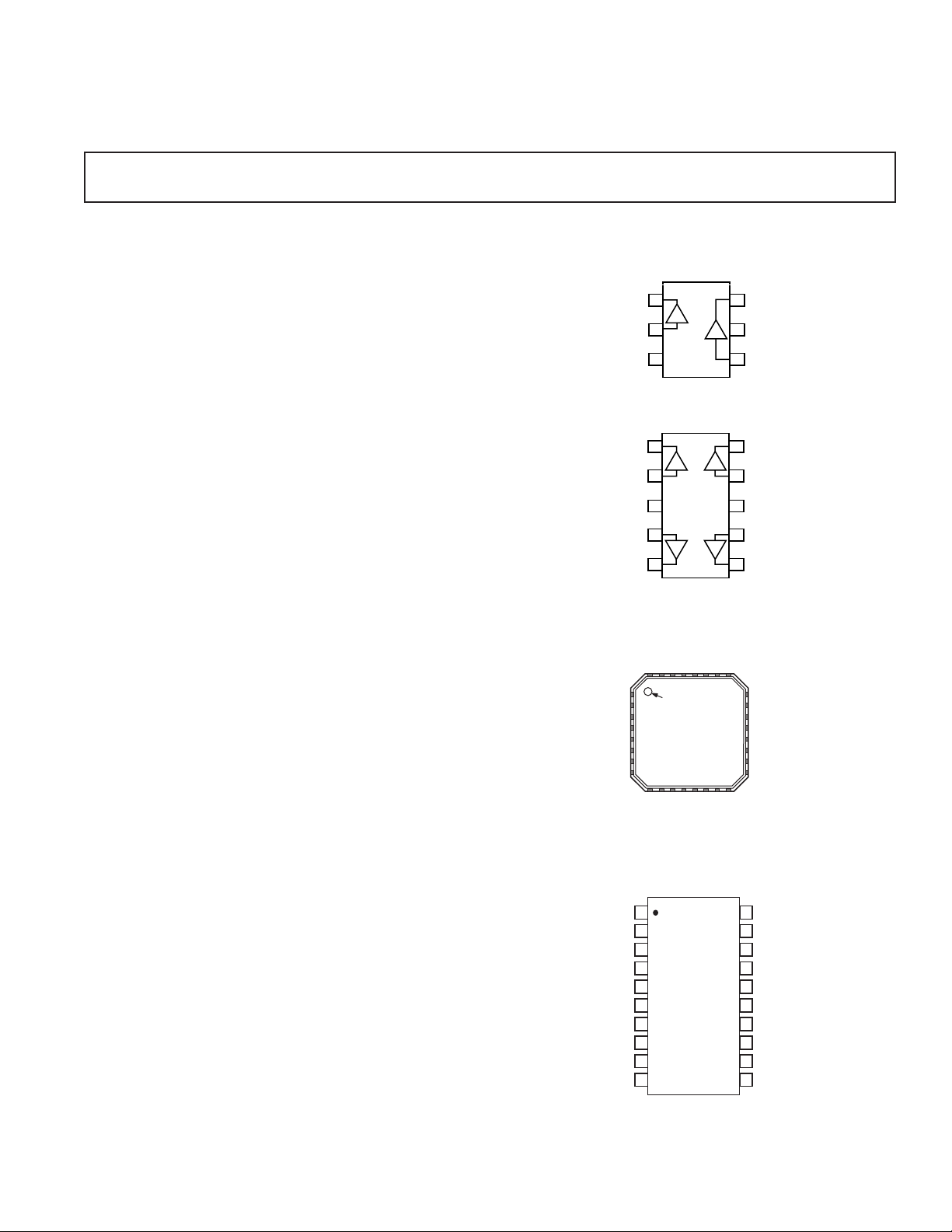
Buffer Amplifiers
AD8568/AD8569/AD8570
PIN CONFIGURATIONS
6-Lead SOT-23
(RT Suffix)
1
OUT B
V+ 1
NC 2
IN C 3
IN D 4
IN E 5
IN F 6
NC 7
V+ 8
OUT A
2
IN A
GND
3
AD8568
10-Lead MSOP
(RM Suffix)
OUT A
1
2
IN A
V+
3
AD8569
4
IN B
56
32-Lead LFCSP
(CP Suffix)
32 NC
31 IN B
30 IN A
29 NC
PIN 1
INDICATOR
AD8570
TOP VIEW
28 NC
27 OUT A
6
OUT B
V+
5
IN B
4
10
OUT D
9
IN D
8
GND
IN C
7
OUT C
26 OUT B
25 NC
24 GND
23 NC
22 OUT C
21 OUT D
20 OUT E
19 OUT F
18 NC
17 GND
REV. C
Information furnished by Analog Devices is believed to be accurate and
reliable. However, no responsibility is assumed by Analog Devices for its
use, nor for any infringements of patents or other rights of third parties that
may result from its use. No license is granted by implication or otherwise
under any patent or patent rights of Analog Devices. Trademarks and
registered trademarks are the property of their respective owners.
NC 9
NC 12
NC 13
OUT H 14
OUT G 15
NC 16
IN H 11
IN G 10
NC = NO CONNECT
20-Lead TSSOP
1
IN 1
2
IN 2
3
V+
4
AD8570-ARU
IN 3
IN 4
IN 5
IN 6
V+
IN 7
IN 8
TOP VIEW
5
6
7
8
9
10
One Technology Way, P.O. Box 9106, Norwood, MA 02062-9106, U.S.A.
Tel: 781/329-4700 www.analog.com
Fax: 781/326-8703 © 2003 Analog Devices, Inc. All rights reserved.
20
OUT 1
19
OUT 2
18
V–
17
OUT 3
16
OUT 4
15
OUT 5
14
OUT 6
13
V–
12
OUT 7
11
OUT 8
Page 2

AD8568/AD8569/AD8570–SPECIFICATIONS
ELECTRICAL CHARACTERISTICS
(4.5 V ≤ VS ≤ 16 V, VCM = VS/2, TA = 25C, unless otherwise noted.)
Parameter Symbol Conditions Min Typ Max Unit
INPUT CHARACTERISTICS
Offset Voltage V
Offset Voltage Drift ∆V
Input Bias Current I
B
OS
/∆T –40°C ≤ TA ≤ +85°C5µV/°C
OS
210mV
80 600 nA
–40°C ≤ TA ≤ +85°C 800 nA
Input Voltage Range –0.5 –V
Input Impedance Z
Input Capacitance C
IN
IN
400 kΩ
1pF
+ 0.5 V
S
OUTPUT CHARACTERISTICS
Output Voltage High V
Output Voltage Low V
Continuous Output Current I
Peak Output Current I
OH
OL
OUT
PK
IL = 100 µAV
= 16 V, IL = 5 mA 15.85 15.95 V
V
S
–40°C ≤ T
= 4.5 V, IL = 5 mA 4.2 4.38 V
V
S
–40°C ≤ T
≤ +85°C 15.75 V
A
≤ +85°C 4.1 V
A
– 0.005 V
S
IL = 100 µA5mV
= 16 V, IL = 5 mA 42 150 mV
V
S
–40°C ≤ T
V
= 4.5 V, IL = 5 mA 95 300 mV
S
–40°C ≤ T
≤ +85°C 250 mV
A
≤ +85°C 400 mV
A
35 mA
VS = 16 V 250 mA
TRANSFER CHARACTERISTICS
Gain A
VCL
RL = 2 kΩ 0.995 0.9985 1.005 V/V
–40°C ≤ T
≤ +85°C 0.995 0.9980 1.005 V/V
A
Gain Linearity NL RL = 2 kΩ, VO = 0.5 to (VS – 0.5 V) 0.01 %
POWER SUPPLY
Supply Voltage V
S
Power Supply Rejection Ratio PSRR V
Supply Current/Amplifier I
SY
= 4 V to 17 V
S
–40°C ≤ T
≤ +85°C7090 dB
A
VO = VS/2, No Load 700 850 µA
4.5 16 V
–40°C ≤ TA ≤ +85°C1mA
DYNAMIC PERFORMANCE
Slew Rate SR RL = 10 kΩ, CL = 200 pF 4 6 V/µs
Bandwidth BW –3 dB, R
Phase Margin Øo R
L
= 10 kΩ, CL = 10 pF 6 MHz
L
= 10 kΩ, CL = 10 pF 65 Degrees
Channel Separation 75 dB
NOISE PERFORMANCE
Voltage Noise Density e
Current Noise Density i
Specifications subject to change without notice.
n
e
n
n
f = 1 kHz 26 nV/√Hz
f = 10 kHz 25 nV/√Hz
f = 10 kHz 0.8 pA/√Hz
–2–
REV. C
Page 3
AD8568/AD8569/AD8570
ABSOLUTE MAXIMUM RATINGS*
Supply Voltage (VS) . . . . . . . . . . . . . . . . . . . . . . . . . . . . . 18 V
Input Voltage . . . . . . . . . . . . . . . . . . . . . . –0.5 V to V
Differential Input Voltage . . . . . . . . . . . . . . . . . . . . . . . . . . V
+ 0.5 V
S
S
Storage Temperature Range . . . . . . . . . . . . –65°C to +150°C
Operating Temperature Range . . . . . . . . . . . –40°C to +85°C
Junction Temperature Range . . . . . . . . . . . . –65°C to +150°C
Lead Temperature Range (Soldering, 60 sec) . . . . . . . . 300°C
*Stresses above those listed under Absolute Maximum Ratings may cause perma-
nent damage to the device. This is a stress rating only; functional operation of the
device at these or any other conditions above those listed in the operational
sections of this specification is not implied. Exposure to absolute maximum rating
conditions for extended periods may affect device reliability.
ORDERING GUIDE
Temperature Package Package Branding
Model Range Description Option Information
AD8568ART-R2 –40°C to +85°C 6-Lead SOT-23 RT-6 AWA
AD8568ART-REEL –40°C to +85°C 6-Lead SOT-23 RT-6 AWA
AD8568ART-REEL7 –40°C to +85°C 6-Lead SOT-23 RT-6 AWA
AD8569ARM-R2 –40°C to +85°C 10-Lead MSOP RM-10 AXA
AD8569ARM-REEL –40°C to +85°C 10-Lead MSOP RM-10 AXA
AD8569ARMZ-REEL* –40°C to +85°C 10-Lead MSOP RM-10 AXA
AD8570ACP-R2 –40°C to +85°C 32-Lead LFCSP CP-32-2
AD8570ACP-REEL –40°C to +85°C 32-Lead LFCSP CP-32-2
AD8570ACP-REEL7 –40°C to +85°C 32-Lead LFCSP CP-32-2
AD8570ARU –40°C to +85°C 20-Lead TSSOP RU-20
AD8570ARU-REEL –40°C to +85°C 20-Lead TSSOP RU-20
*Z = Pb-free part.
Package Type
1
JA
JC
2
Unit
JB
6-Lead SOT-23 (RT) 250 140 °C/W
10-Lead MSOP (RM) 200 44 °C/W
20-Lead TSSOP (RU) 72 45 °C/W
32-Lead LFCSP (CP) 35 13 °C/W
NOTES
1
θJA is specified for worst-case conditions, i.e., θ
onto a circuit board for surface-mount packages.
2
⌿JB is applied for calculating the junction temperature by reference to the board
temperature.
is specified for a device soldered
JA
CAUTION
ESD (electrostatic discharge) sensitive device. Electrostatic charges as high as 4000 V readily
accumulate on the human body and test equipment and can discharge without detection. Although
the AD8568/AD8569/AD8570 features proprietary ESD protection circuitry, permanent damage
may occur on devices subjected to high energy electrostatic discharges. Therefore, proper ESD
precautions are recommended to avoid performance degradation or loss of functionality.
WARNING!
ESD SENSITIVE DEVICE
REV. C
–3–
Page 4
AD8568/AD8569/AD8570
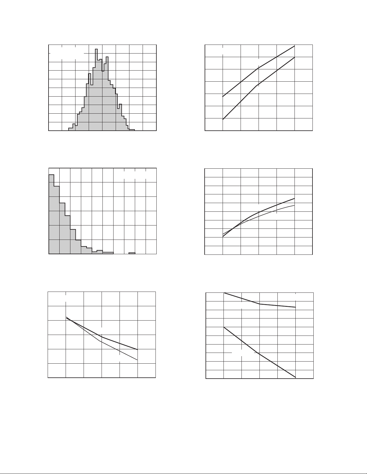
–Typical Performance Characteristics
100
TA = 25C
90
4.5V < V
< 16V
S
80
70
60
50
40
30
QUANTITY (Amplifiers)
20
10
0
12 9
6 3
INPUT OFFSET VOLTAGE (mV)
0 36912
TPC 1. Input Offset Voltage Distribution
300
4.5V < VS < 16V
250
200
150
100
QUANTITY (Amplifiers)
50
0
0 10010
20 30 40 50 60 70 80 90
TCVOS (V/C)
TPC 2. Input Offset Voltage Drift Distribution
0
VCM = VS/2
50
100
150
200
250
INPUT BIAS CURRENT (nA)
300
350
40
VS = 16V
VS = 4.5V
25 85
TEMPERATURE (C)
TPC 4. Input Bias Current vs. Temperature
5
4
3
2
1
0
1
2
INPUT OFFSET CURRENT (nA)
3
4
5
40
VS = 4.5V
VS = 16V
25 85
TEMPERATURE (C)
TPC 5. Input Offset Current vs. Temperature
0
VCM = VS/2
0.25
0.50
0.75
1.00
INPUT OFFSET VOLTAGE (mV)
1.25
1.50
40
VS = 16V
VS = 4.5V
25 85
TEMPERATURE (C)
TPC 3. Input Offset Voltage vs. Temperature
–4–
15.96
15.95
15.94
15.93
15.92
15.91
15.90
15.89
OUTPUT VOLTAGE SWING (V)
15.88
15.87
15.86
VS = 16V
VS = 4.5V
40
25 85
TEMPERATURE (C)
I
LOAD
= 5mA
TPC 6. Output Voltage Swing vs. Temperature
4.46
4.45
4.44
4.43
4.42
4.41
4.40
4.39
4.38
4.37
4.36
REV. C
Page 5

150
TEMPERATURE (C)
0.80
0.50
40
SUPPLY CURRENT/AMPLIFIER (mA)
25 85
0.65
0.60
0.55
VS = 16V
VS = 4.5V
0.70
VCM = VS/2
0.75
TEMPERATURE (C)
7
0
40
SLEW RATE (V/s)
25 85
3
2
1
VS = 16V
VS = 4.5V
4
RL = 10k
C
L
= 200pF
5
6
SUPPLY VOLTAGE (V)
1.0
0
0182
SUPPLY CURRENT/AMPLIFIER (mA)
4681012 14 16
0.9
0.5
0.3
0.2
0.1
0.8
0.7
0.4
0.6
TA = 25C
A
V
= +1
V
O
= VS/2
I
= 5mA
LOAD
135
120
105
90
75
60
45
30
OUTPUT VOLTAGE SWING (mV)
15
0
40
AD8568/AD8569/AD8570
VS = 4.5V
VS = 16V
25 85
TEMPERATURE (C)
TPC 7. Output Voltage Swing vs. Temperature
0.9999
0.9997
GAIN ERROR (V/V)
4.5V < VS < 16V
= 0.5V TO 15V
V
OUT
RL = 2k
RL = 600
0.9995
40
25 85
TEMPERATURE (C)
TPC 8. Voltage Gain vs. Temperature
1k
TA = 25C
100
VS = 4.5V
TPC 10. Supply Current/Amplifier vs. Temperature
TPC 11. Slew Rate vs. Temperature
10
OUTPUT VOLTAGE (mV)
1
0.1
0.001 1000.01
TPC 9. Output Voltage to Supply Rail vs. Load Current
REV. C
LOAD CURRENT (mA)
VS = 16V
0.1 1 10
TPC 12. Supply Current/Amplifier vs. Supply Voltage
–5–
Page 6

AD8568/AD8569/AD8570
10
5
0
5
10
15
GAIN (dB)
20
25
TA = 25C
= 8V
V
S
30
35
40
= 50mV rms
V
IN
= 40pF
C
L
= +1
A
V
100k 100M
560
FREQUENCY (Hz)
1k
10k
150
10M1M
TPC 13. Frequency Response vs. Resistive Loading
25
TA = 25C
= 8V
V
20
S
= 50mV rms
V
IN
15
= 10k
R
L
= +1
A
V
10
5
0
GAIN (dB)
5
10
15
20
25
100k 100M
1040pF
540pF
FREQUENCY (Hz)
50pF
100pF
10M1M
TPC 14. Frequency Response vs. Capacitive Loading
18
16
14
12
10
8
6
OUTPUT SWING (V p-p)
TA = 25C
4
= 16V
V
S
A
= +1
V
= 10k
R
2
L
DISTORTION < 1%
0
FREQUENCY (Hz)
10M1M100k10k1k10010
TPC 16. Closed-Loop Output Swing vs. Frequency
160
TA = 25C
140
= 16V
V
S
120
100
80
60
40
20
0
POWER SUPPLY REJECTION RATIO (dB)
20
40
100 10M1k
+PSRR
PSRR
10k 100k 1M
FREQUENCY (Hz)
TPC 17. Power Supply Rejection Ratio vs. Frequency
500
450
400
350
300
250
200
IMPEDANCE ()
150
100
50
0
100 10M1k
10k 100k 1M
FREQUENCY (Hz)
VS = 4.5V
VS = 16V
TPC 15. Closed-Loop Output Impedance vs. Frequency
160
TA = 25C
140
= 4.5V
V
S
120
100
80
60
40
20
0
POWER SUPPLY REJECTION RATIO (dB)
20
40
+PSRR
PSRR
100 10M1k
10k 100k 1M
FREQUENCY (Hz)
TPC 18. Power Supply Rejection Ratio vs. Frequency
–6–
REV. C
Page 7

AD8568/AD8569/AD8570
1,000
TA = 25C
VS 16V
4.5V
100
10
VOLTA G E NOISE DENSITY (nV/ Hz)
1
10 10k100
FREQUENCY (Hz)
1k
TPC 19. Voltage Noise Density vs. Frequency
20
TA = 25C
0
20
40
60
80
100
120
CHANNEL SEPARATION (dB)
140
160
180
4.5V < V
< 16V
S
FREQUENCY (Hz)
TPC 20. Channel Separation vs. Frequency
100
TA = 25C
90
V
= 4.5V
S
= 2.25V
V
CM
80
V
= 100mV p-p
IN
= +1
A
V
70
R
= 10k
L
60
50
40
OVERSHOOT (%)
30
20
10
0
10 1k100
LOAD CAPACITANCE (pF)
OS
+OS
TPC 22. Small Signal Overshoot vs. Load Capacitance
15
TA = 25C
VS = 8V
10
= 10k
R
V
OUTPUT SWING FROM 0V TO
100M10M1M100k10k1k100
L
5
0
5
UNDERSHOOT SETTLING TO 0.1%
10
15
02.00.5
OVERSHOOT SETTLING TO 0.1%
1.0 1.5
SETTLING TIME (s)
TPC 23. Settling Time vs. Step Size
100
TA = 25C
90
V
= 16V
S
= 8V
V
CM
80
V
= 100mV p-p
IN
= +1
A
V
70
R
= 10k
L
60
50
40
OVERSHOOT (%)
30
20
10
0
10 1k100
LOAD CAPACITANCE (pF)
OS
+OS
TPC 21. Small Signal Overshoot vs. Load Capacitance
REV. C
–7–
0
0
0
0
0
0
VOLTA GE (3V/DIV)
0
0
0
000
000000
TIME (2s/DIV)
TA = 25C
VS = 16V
= +1
A
V
RL = 10k
= 300pF
C
L
TPC 24. Large Signal Transient Response
Page 8

AD8568/AD8569/AD8570
0
0
0
0
0
0
VOLTA GE (1V/DIV)
0
0
0
000
000000
TIME (2s/DIV)
TA = 25C
= 4.5V
V
S
= +1
A
V
= 10k
R
L
= 300pF
C
L
TPC 25. Large Signal Transient Response
0
0
0
0
0
TA = 25C
= 16V
V
S
= +1
A
V
= 10k
R
L
= 100pF
C
L
0
0
0
0
0
0
VOLTA GE (50mV/DIV)
0
0
0
000
000000
TIME (1s/DIV)
TA = 25C
= 4.5V
V
S
= +1
A
V
= 10k
R
L
= 100pF
C
L
TPC 27. Small Signal Transient Response
0
0
0
0
0
TA = 25C
= 16V
V
S
= +1
A
V
= 10k
R
L
0
VOLTA GE (50mV/DIV)
0
0
0
000
000000
TIME (1s/DIV)
TPC 26. Small Signal Transient Response
0
VOLTA GE (3V/DIV)
0
0
0
000
000000
TIME (40s/DIV)
TPC 28. No Phase Reversal
–8–
REV. C
Page 9

AD8568/AD8569/AD8570
AMBIENT TEMPERATURE – C
1.00
0.75
0
35
85
15
MAXIMUM POWER DISSIPATION – W
5254565
0.50
0.25
10-LEAD MSOP
6-LEAD SOT-23
APPLICATIONS
Theory of Operation
This family of buffers is designed to drive large capacitive loads in
LCD applications. Each has high output current drive and railto-rail input/output operation and can be powered from a single
16 V supply. They are also intended for other applications where
low distortion and high output current drive are needed.
Input Overvoltage Protection
As with any semiconductor device, whenever the input exceeds
either supply voltage, attention needs to be paid to the input
overvoltage characteristics. As an overvoltage occurs, the amplifier
could be damaged, depending on the voltage level and the magnitude
of the fault current. When the input voltage exceeds either supply
by more than 0.6 V, the internal pn junctions will allow current
to flow from the input to the supplies.
This input current is not inherently damaging to the device as
long as it is limited to 5 mA or less. If a condition exists using the
buffers where the input exceeds the supply by more than 0.6 V,
an external series resistor should be added. The size of the resistor can be calculated by using the maximum overvoltage divided
by 5 mA. This resistance should be placed in series with the input
exposed to an overvoltage.
Output Phase Reversal
The buffer family is immune to phase reversal. Although the
device’s output will not change phase, large currents due to input
overvoltage could damage the device. In applications where
the possibility exists of an input voltage exceeding the supply
voltage, overvoltage protection should be used as described in
the previous section.
Power Dissipation
The maximum allowable internal junction temperature of 150°C
limits the device’s maximum power dissipation. As the ambient
temperature increases, the maximum power dissipated by the
device must decrease linearly to maintain the maximum junction temperature. If this maximum junction temperature is
exceeded momentarily, the device will still operate properly once
the junction temperature is reduced below 150°C. If the maximum
junction temperature is exceeded for an extended period of time,
overheating could lead to permanent damage of the device.
The maximum safe junction temperature, T
the following formula, we can obtain the maximum power that
the buffer family can safely dissipate as a function of temperature.
where:
= the power dissipation.
P
DISS
= the maximum allowable junction temperature
T
J
MAX
(150°C).
= the ambient temperature of the circuit.
T
A
= the AD856x package thermal resistance,
θ
J
A
junction-to-ambient.
The power dissipated by the device can be calculated as
where:
= the supply voltage.
V
S
V
= the output voltage.
OUT
= the output load current.
I
LOAD
REV. C
, is 150°C. Using
JMAX
PTT
=−
()
DISS A A
PVV I
DISS S OUT LOAD
JMAX J
=−
()
/ θ
×
Figure 1 shows the maximum power dissipation versus temperature.
To achieve proper operation, use the previous equation to calculate
for a specific package at any given temperature, or see Figure 1.
P
DISS
Figure 1. Maximum Power Dissipation vs. Temperature
for 6- and 10-Lead Packages
Total Harmonic Distortion + Noise (THD+N)
The buffer family features low THD+N. The total harmonic
distortion plus noise for the buffer over the entire supply range
is below 0.08%. When the device is powered from a 16 V supply,
the THD+N stays below 0.03%. Figure 2 shows the AD8568
THD+N versus frequency performance.
10
1
THD + N – %
0.1
0.01
20 30k
VS = 2.5V
100
VS = 8V
1k 10k
FREQUENCY – Hz
Figure 2. AD8568 THD+N vs. Frequency
Short-Circuit Output Conditions
The buffer family does not have internal short-circuit protection
circuitry. As a precautionary measure, do not short the output
directly to the positive power supply or to ground.
It is not recommended to operate the AD856x with more than
35 mA of continuous output current. The output current can be
limited by placing a series resistor at the output of the amplifier
whose value can be derived using the following equation.
V
R
X
S
≥
35
mA
For a 5 V single-supply operation, RX should have a minimum
value of 143 Ω.
–9–
Page 10

AD8568/AD8569/AD8570
OUTLINE DIMENSIONS
6-Lead Small Outline Transistor Package [SOT-23]
(RT-6)
Dimensions shown in millimeters
2.90 BSC
2
1.90
BSC
0.50
0.30
4 5
0.95 BSC
2.80 BSC
1.45 MAX
SEATING
PLANE
0.22
0.08
10
0.60
4
0.45
0
0.30
1.60 BSC
1.30
1.15
0.90
0.15 MAX
6
1 3
PIN 1
COMPLIANT TO JEDEC STANDARDS MO-178AB
32-Lead Lead Frame Chip Scale Package [LFCSP]
Dimensions shown in millimeters
3.00 BSC
3.00 BSC
0.95
0.85
0.75
5 x 5 mm Body
(CP-32-2)
10-Lead Micro Small Outline Package [MSOP]
(RM-10)
Dimensions shown in millimeters
6
10
4.90 BSC
1
5
PIN 1
0.50 BSC
1.10 MAX
0.15
0.00
COPLANARITY
0.10
0.27
0.17
COMPLIANT TO JEDEC STANDARDS MO-187BA
SEATING
PLANE
0.23
0.08
8
0
0.80
0.60
0.40
PIN 1
INDICATOR
1.00
0.85
0.80
12 MAX
SEATING
PLANE
5.00
BSC SQ
TOP
VIEW
0.80 MAX
0.65 TYP
0.30
0.23
0.18
COMPLIANT TO JEDEC STANDARDS MO-220-VHHD-2
4.75
BSC SQ
0.20 REF
0.05 MAX
0.02 NOM
0.60 MAX
0.50
BSC
0.50
0.40
0.30
COPLANARITY
0.08
0.60 MAX
25
24
17
16
BOTTOM
VIEW
32
1
9
8
3.50 REF
PIN 1
INDICATOR
3.25
SQ
3.10
2.95
0.25 MIN
–10–
REV. C
Page 11

AD8568/AD8569/AD8570
OUTLINE DIMENSIONS
20-Lead Thin Shrink Small Outline Package [TSSOP]
(RU-20)
Dimensions shown in millimeters
6.60
6.50
6.40
PIN 1
0.15
0.05
COPLANARITY
0.10
20
1
0.30
0.19
COMPLIANT TO JEDEC STANDARDS MO-153AC
0.65
BSC
11
10
1.20
MAX
SEATING
PLANE
4.50
4.40
4.30
6.40 BSC
0.20
0.09
8
0
0.75
0.60
0.45
Revision History
Location Page
12/03—Data Sheet changed from REV. B to REV. C.
Updated ORDERING GUIDE . . . . . . . . . . . . . . . . . . . . . . . . . . . . . . . . . . . . . . . . . . . . . . . . . . . . . . . . . . . . . . . . . . . . . . . . . . . . . 3
Updated OUTLINE DIMENSIONS . . . . . . . . . . . . . . . . . . . . . . . . . . . . . . . . . . . . . . . . . . . . . . . . . . . . . . . . . . . . . . . . . . . . . . . 10
5/02—Data Sheet changed from REV. A to REV. B.
Added 20-Lead TSSOP Package . . . . . . . . . . . . . . . . . . . . . . . . . . . . . . . . . . . . . . . . . . . . . . . . . . . . . . . . . . . . . . . . . . . . . . . . . . . . 1
Added Package Type . . . . . . . . . . . . . . . . . . . . . . . . . . . . . . . . . . . . . . . . . . . . . . . . . . . . . . . . . . . . . . . . . . . . . . . . . . . . . . . . . . . . . 3
Updated ORDERING GUIDE . . . . . . . . . . . . . . . . . . . . . . . . . . . . . . . . . . . . . . . . . . . . . . . . . . . . . . . . . . . . . . . . . . . . . . . . . . . . . 3
Added TSSOP Package to OUTLINE DIMENSIONS . . . . . . . . . . . . . . . . . . . . . . . . . . . . . . . . . . . . . . . . . . . . . . . . . . . . . . . . . . 10
REV. C
–11–
Page 12

C02612–0–12/03(C)
–12–
 Loading...