


1.8 V to 5 V Auto-Zero, In-Amp
www.BDTIC.com/ADI
FEATURES
Low offset voltage: 20 μV max
Low input offset drift: 0.1 μV/°C max
High CMR: 120 dB min @ G = 100
Low noise: 0.7 μV p-p from 0.01 Hz to 10 Hz
Wide gain range: 0.1 to 10,000
Single-supply operation: 1.8 V to 5.5 V
Rail-to-rail output
Shutdown capability
APPLICATIONS
Strain gauge
Weigh scales
Pressure sensors
Laser diode control loops
Portable medical instruments
Thermocouple amplifiers
with Shutdown
AD8553
PIN CONFIGURATION
RGA
1
2
VINP
VCC
VFB
AD8553
3
TOP VIEW
(Not to Scale)
VO
4
5
Figure 1. 10-Lead MSOP
10
9
8
7
6
RGB
VINN
GND
V
REF
ENABLE
05474-001
GENERAL DESCRIPTION
The AD85531 is a precision instrumentation amplifier featuring
low noise, rail-to-rail output and a power-saving shutdown
mode. The AD8553 also features low offset voltage and drift
coupled with high common-mode rejection. In shutdown
mode, the total supply current is reduced to less than 4 µA.
The AD8553 is capable of operating from 1.8 V to 5.5 V.
With a low offset voltage of 20 µV, an offset voltage drift of
0.1 µV/°C, and
10 Hz), the AD8553 is ideal for applications where error sources
cannot be tolerated. Precision instrumentation, position and
pressure sensors, medical instrumentation, and strain gauge
amplifiers benefit from the low noise, low input bias current,
and high common-mode rejection. The small footprint and low
cost are ideal for high volume applications.
a voltage noise of only 0.7 µV p-p (0.01 Hz to
The small package and low power consumption allow
max
imum channel density and minimum board size for
space-critical equipment and portable systems.
The AD8553 is specified over the industrial temperature range
rom −40°C to +85°C. The AD8553 is available in a Pb-free,
f
10-lead MSOP.
1
Patent pending.
Rev. 0
Information furnished by Analog Devices is believed to be accurate and reliable. However, no
responsibility is assumed by Anal og Devices for its use, nor for any infringements of patents or ot her
rights of third parties that may result from its use. Specifications subject to change without notice. No
license is granted by implication or otherwise under any patent or patent rights of Analog Devices.
Trademarks and registered trademarks are the property of their respective owners.
One Technology Way, P.O. Box 9106, Norwood, MA 02062-9106, U.S.A.
Tel: 781.329.4700 www.analog.com
Fax: 781.461.3113 © 2005 Analog Devices, Inc. All rights reserved.

AD8553
www.BDTIC.com/ADI
TABLE OF CONTENTS
Features .............................................................................................. 1
Gain Selection (Gain-Setting Resistors).................................. 12
Applications....................................................................................... 1
Pin Configuration............................................................................. 1
General Description......................................................................... 1
Revision History ............................................................................... 2
Specifications..................................................................................... 3
Electrical Characteristics............................................................. 3
Absolute Maximum Ratings............................................................ 5
Thermal Resistance ...................................................................... 5
ESD Caution.................................................................................. 5
Typical Performance Characteristics ............................................. 6
Theory of Operation ...................................................................... 11
High PSR and CMR ................................................................... 11
1/f Noise Correction ..................................................................11
Applications..................................................................................... 12
Reference Connection ............................................................... 12
Disable Function ........................................................................ 12
Output Filtering.......................................................................... 12
Clock Feedthrough..................................................................... 12
Low Impedance Output............................................................. 12
Maximizing Performance Through Proper Layout ............... 13
Power Supply Bypassing ............................................................ 13
Input Overvoltage Protection................................................... 13
Capacitive Load Drive ............................................................... 13
Circuit Diagrams/Connections................................................ 14
Outline Dimensions ....................................................................... 18
Ordering Guide............................................................................... 18
REVISION HISTORY
10/05—Revision 0: Initial Version
Rev. 0 | Page 2 of 20

AD8553
www.BDTIC.com/ADI
SPECIFICATIONS
ELECTRICAL CHARACTERISTICS
VCC = 5.0 V, VCM = 2.5 V, V
resistor values. Temperature specifications guaranteed by characterization.
Table 1.
Parameter Symbol Conditions Min Typ Max Unit
INPUT CHARACTERISTICS
Input Offset Voltage V
G = 100 4 20 μV
G = 10 15 50 μV
G = 1 120 375 μV
vs. Temperature ΔVOS/ΔT G = 1000, −40°C ≤ TA ≤ +85°C 0.02 0.1 μV/°C
G = 100, −40°C ≤ TA ≤ +85°C 0.02 0.1 μV/°C
G = 10, −40°C ≤ TA ≤ +85°C 0.1 0.3 μV/°C
G = 1, −40°C ≤ TA ≤ +85°C 1 3 μV/°C
Input Bias Current I
−40°C ≤ TA ≤ +85°C 2 nA
Input Offset Current I
VREF Pin Current I
Input Operating Impedance
Differential 50||1 MΩ||pF
Common Mode 10||10 GΩ||pF
Input Voltage Range 0 3.3 V
Common-Mode Rejection CMR G = 100, VCM = 0 V to 3.3 V, −40°C ≤ TA ≤ +85°C 120 140 dB
G = 10, VCM = 0 V to 3.3 V, −40°C ≤ TA ≤ +85°C 100 120 dB
Gain Error G = 100, VCM = 12.125 mV, VO = 0.075 V to 4.925 V 0.10 0.3 %
G = 10, VCM = 121.25 mV , VO = 0.075 V to 4.925 V 0.15 0.4 %
Gain Drift G = 10, 100, 1000, −40°C ≤ TA ≤ +85°C 5 25 ppm/°C
G = 1, −40°C ≤ TA ≤ +85°C 30 50 ppm/°C
Nonlinearity G = 100, VCM = 12.125 mV, VO = 0.075 V to 4.925 V 0.001 0.003 % FS
G = 10, VCM = 121.25 mV, VO = 0.075 V to 4.925 V 0.040 0.060 % FS
V
Range 0.8 4.2 V
REF
OUTPUT CHARACTERISITICS
Output Voltage High V
Output Voltage Low V
Short-Circuit Current I
POWER SUPPLY
Power Supply Rejection PSR G = 100, VS = 1.8 V to 5.5 V, VCM = 0 V 100 120 dB
G = 10, VS = 1.8 V to 5.5 V, VCM = 0 V 90 110 dB
Supply Current I
−40°C ≤ TA ≤ +85°C 1.5 mA
Supply Current Shutdown Mode I
ENABLE INPUTS
Logic High Voltage 2.40 V
Logic Low Voltage 0.80 V
NOISE PERFORMANCE
Voltage Noise e
Voltage Noise Density e
G = 10, f = 1 kHz 150 nV/√Hz
Internal Clock Frequency 60 kHz
Signal Bandwidth
1
Higher bandwidths result in higher noise.
1
= VCC/2, VIN = V
REF
G = 1 to 1000 1 kHz
B
OS
REF
SC
SY
SD
OS
OH
OL
n p-p
n
− V
, R
INP
INN
G = 1000 4 20 μV
0.4 1 nA
2 nA
0.01 1 nA
4.925 V
0.075 V
±35 mA
IO = 0 mA, VIN = 0 V 1.1 1.3 mA
2 4 μA
f = 0.01 Hz to 10 Hz 0.7 μV p-p
G = 100, f = 1 kHz 30 nV/√Hz
= 10 kΩ, TA = 25°C, G = 100, unless specified. See Tab l e 5 for gain setting
LOAD
Rev. 0 | Page 3 of 20

AD8553
www.BDTIC.com/ADI
= 1.8 V, VCM = -0 V, V
V
S
= VS/2, VIN = V
REF
INP
− V
INN
, R
= 10 kΩ, TA = 25°C, G = 100, unless specified. See Ta b le 5 for gain setting
LOAD
resistor values. Temperature specifications guaranteed by characterization.
Table 2.
Parameter Symbol Conditions Min Typ Max Unit
INPUT CHARACTERISTICS
Input Offset Voltage V
OS
G = 1000 3 20 μV
G = 100 3 20 μV
G = 10 14 50 μV
G = 1 130 375 μV
Vs. Temperature ΔVOS/ΔT G = 1000, −40°C ≤ TA ≤ +85°C 0.02 0.25 μV/°C
G = 100, −40°C ≤ TA ≤ +85°C 0.02 0.25 μV/°C
G = 10, −40°C ≤ TA ≤ +85°C 0.1 3 μV/°C
G = 1, −40°C ≤ TA ≤ +85°C 1 10 μV/°C
Input Bias Current I
B
0.05 1 nA
−40°C ≤ TA ≤ +85°C 2 nA
Input Offset Current I
VREF Pin Current I
OS
REF
2 nA
0.02 1 nA
Input Operating Impedance
Differential 50||1 MΩ||pF
Common Mode 10||10 GΩ||pF
Input Voltage Range 0 0.15 V
Common-Mode Rejection CMR G = 100, VCM = 0 V to 0.15 V, −40°C ≤ TA ≤ +85°C 100 110 dB
G = 10, VCM = 0 V to 0.15 V, −40°C ≤ TA ≤ +85°C 90 110 dB
Gain Error G = 100, VCM =4.125 mV, VO = 0.075 V to 1.725 V 0.2 0.4 %
G = 10, VCM = 41.25 mV, VO = 0.075 V to 1.725 V 0.2 0.4 %
Gain Drift G = 10, 100, 1000, −40°C ≤ TA ≤ +85°C 25 ppm/°C
G = 1, −40°C ≤ TA ≤ +85°C 50 ppm/°C
Nonlinearity G = 100, VCM = 4.125 mV, VO = 0.075 V to 1.725 V 0.003 % FS
G = 10, VCM = 41.25 mV, VO = 0.075 V to 1.725 V 0.010 % FS
V
Range 0.8 1.0 V
REF
OUTPUT CHARACTERISITICS
Output Voltage High V
Output Voltage Low V
Short-Circuit Current I
OH
OL
SC
1.725 V
0.075 V
±5 mA
POWER SUPPLY
Power Supply Rejection PSR G = 100, VS = 1.8 V to 5.5 V, VCM = 0 V 100 120 dB
Supply Current I
SY
IO = 0 mA, VIN = 0 V 0.8 1.2 mA
−40°C ≤ TA ≤ +85°C 1.4 mA
Supply Current Shutdown Mode I
SD
2 4 μA
ENABLE INPUTS
Logic High Voltage 1.4 V
Logic Low Voltage 0.5 V
NOISE PERFORMANCE
Voltage Noise e
Voltage Noise Density e
n p-p
n
f = 0.01 Hz to 10 Hz 0.7 μV p-p
G = 100, f = 1 kHz 30 nV/√Hz
G = 10, f = 1 kHz 150 nV/√Hz
Internal Clock Frequency 60 kHz
Signal Bandwidth
1
Higher bandwidths result in higher noise.
1
G = 1 to 1000 1 kHz
Rev. 0 | Page 4 of 20

AD8553
www.BDTIC.com/ADI
ABSOLUTE MAXIMUM RATINGS
Table 3.
Parameter Ratings
Supply Voltage 6 V
Input Voltage +V
Differential Input Voltage
Output Short-Circuit Duration to GND Indefinite
Storage Temperature Range (RM Package) −65°C to +150°C
Operating Temperature Range −40°C to +85°C
Junction Temperature Range (RM Package) −65°C to +150°C
Lead Temperature Range (Soldering, 10 sec) 300°C
1
Differential input voltage is limited to ±5.0 V, the supply voltage, or
whichever is less.
1
±V
SUPPLY
SUPPLY
Stresses above those listed under Absolute Maximum Ratings
may cause permanent damage to the device. This is a stress
rating only; functional operation of the device at these or any
other conditions above those indicated in the operational
section of this specification is not implied. Exposure to absolute
maximum rating conditions for extended periods may affect
device reliability.
THERMAL RESISTANCE
θ JA is specified for the worst-case conditions, that is, a device
soldered in a circuit board for surface-mount packages.
Table 4.
Package Type θ
10-Lead MSOP (RM) 110 32.2 °C/W
1
θJA is specified for the nominal conditions, that is, θJA is specified for the
device soldered on a circuit board.
1
JA
θ
JC
Unit
ESD CAUTION
ESD (electrostatic discharge) sensitive device. Electrostatic charges as high as 4000 V readily accumulate on
the human body and test equipment and can discharge without detection. Although this product features
proprietary ESD protection circuitry, permanent damage may occur on devices subjected to high energy
electrostatic discharges. Therefore, proper ESD precautions are recommended to avoid performance
degradation or loss of functionality.
Rev. 0 | Page 5 of 20

AD8553
√
www.BDTIC.com/ADI
TYPICAL PERFORMANCE CHARACTERISTICS
TA = 25°C, G = 100, unless specified, see Tab l e 5 for gain setting resistor values. Filters as noted are the combination of R2/C2 and R3/C3
as in Figure 31.
80
GAIN = 1000
60
VCC = 1.8V AND 5V
FILTER = 1kHz
80
GAIN = 1000
60
VCC = 1.8V AND 5V
FILTER = 10kHz
GAIN = 100
40
GAIN = 10
20
GAIN (dB)
GAIN = 1
0
–20
–40
10 100 1k 10k 100k
FREQUENCY ( Hz)
Figure 2. Gain vs. Frequency
180
VCC = 5V
FILTER = 1kHz
160
GAIN = 100
140
GAIN = 10
120
GAIN = 1
100
CMR (dB)
80
60
40
20
10 100 1k 10k 100k
FREQUENCY ( Hz)
Figure 3. Common-Mode Rejection (CMR) vs. Frequency
160
GAIN = 100
140
GAIN = 10
120
GAIN = 1
100
80
PSR (dB)
60
40
GAIN = 100
40
GAIN = 10
20
GAIN (dB)
GAIN = 1
0
–20
05474-002
–40
10 100 1k 10k 100k
FREQUENCY ( Hz)
05474-003
Figure 5. Gain vs. Frequency
180
VCC = 5V
FILTER = 10kHz
160
GAIN = 100
140
GAIN = 10
120
GAIN = 1
100
CMR (dB)
80
60
40
05474-004
20
10 100 1k 10k 100k
FREQUENCY ( Hz)
05474-005
Figure 6. Common-Mode Rejection (CMR) vs. Frequency
10k
GAIN = 1
1k
Hz)
100
NOISE (nV/
10
GAIN = 10
GAIN = 100, 1000
20
FILTE R = 10kHz
FILTER = 1kHz
10
10 100 1k 10k 100k
FREQUENCY (Hz)
Figure 4. Power Supply Rejection vs. Frequency
VCC=5VAND1.8V
05474-006
1
0.01 1001010.1 1k 10k 100k
Figure 7. Voltage Noise Density
Rev. 0 | Page 6 of 20
FREQUENCY (Hz)
05474-007
AD8553
V
V
www.BDTIC.com/ADI
VCC=5V
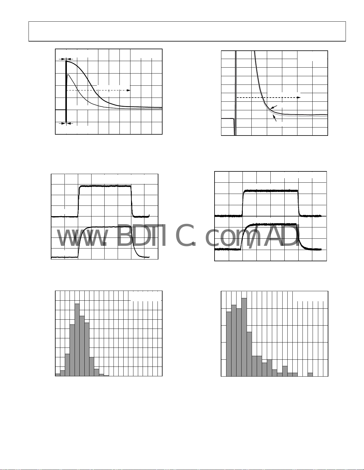
TURN ON TIME = 10µs
FILTER SETTLING
20µV/DI
V
CC
TURN ON TIME = 15µs
V
=1.8V
CC
–0.1 0 0.1 0.2 0. 3 0.4 0.5 0.6 0. 7 0.8 0.9
VCC=5V
=1.8V
TIME (ms)
GAIN = 100
FILTER = 1kHz
Figure 8. Input Offset Voltage vs. Turn-On Time
05474-008
80
70
60
50
40
30
20
10
0
INPUT OFFSET VOLTAGE (µV)
–10
–20
03
50 100 150 200 250 300
FILTER SETTLING
VCC=5V
VCC=1.8V
TIME (µs)
GAIN = 100
FILTER = 10kHz
05474-009
50
Figure 11. Input Offset Voltage vs. Turn-On Time
10kHz FIL TER
50mV/DI
1kHz FIL TER
POPULATION
VCC= 5V, G = 1 , 10, 100, 1000
V
= 1.8V, G = 1, 10, 100, 1000
CC
500µs/DIV
Figure 9. Small Signal Step Response
VCC=5V
GAIN = 100, 1000
VCC = 5V, G = 1, 10, 100, 1000
10kHz FILT ER
1V/DIV
05474-010
1kHz FILT ER
500µs/DIV
05474-011
Figure 12. Large Signal Step Response
VCC=5V
GAIN = 100, 1000
POPULATION
05474-017
16 18
Figure 10. Input Offset Voltage (μV)
200 2 4 6 8 101214
0 0.01 0.02 0.03 0.04 0.05 0.06 0.07 0.08 0.09 0.10
Figure 13. Input Offset Voltage Drift (μV/°C)
Rev. 0 | Page 7 of 20
05474-014

AD8553
www.BDTIC.com/ADI
VCC = 5V
GAIN = 10
VCC = 5V
GAIN = 10
POPULATION
0 5.0 10.0 15.0 20.0 25.0 30.0 35.0 40.0 45.0 50.0
Figure 14. Input Offset Voltage (μV)
POPULATION
–50 –10 30 70 110 150 190 230 270 310 350
Figure 15. Input Offset Voltage (μV)
VCC = 5V
GAIN = 1
POPULATION
05474-016
0 0.03 0.06 0.09 0.12 0.15 0.18 0.21 0.24 0.27 0.30
05474-013
Figure 17. Input Offset Voltage Drift (μV/°C)
VCC = 5V
GAIN = 1
POPULATION
05474-015
0 0.30 0.60 0.90 1.20 1.50 1.80 2.10 2.40 2.70 3.00
05474-012
Figure 18. Input Offset Voltage Drift (μV/°C)
VCC = 5V
GAIN = 100
= 12.125mV
V
CM
POPULATION
–250 –225 –200 –175 –150 –125 –100 –75 –50 –25 0
Figure 16. Gain Error (m%)
05474-020
POPULATION
0 0.3 0.6 0.9 1.2 1.5 1.8 2.1 2.4 2.7 3.0
Figure 19. Nonlinearity (m%)
Rev. 0 | Page 8 of 20
VCC = 5V
GAIN = 100
V
= 12.125mV
CM
05474-019
AD8553
www.BDTIC.com/ADI
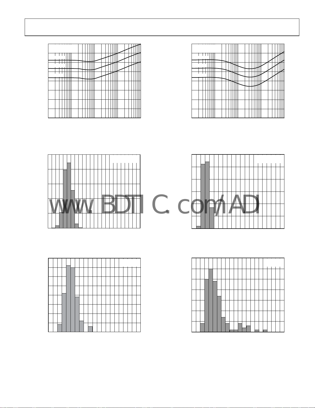
180
160
140
120
100
CMR (dB)
80
VCC = 1.8V
FILTE R = 1kHz
GAIN = 100
GAIN = 10
GAIN = 1
180
160
140
120
100
CMR (dB)
80
VCC = 1.8V
FILTER = 10kHz
GAIN = 100
GAIN = 10
GAIN = 1
60
40
20
10 100 1k 10k 100k
FREQUENCY ( Hz)
Figure 20. Common-Mode Rejection (CMR) vs. Frequency
VCC=1.8V
GAIN = 100, 1000
POPULATION
–2 0 4 6 8 10 12 14 16 18 20
2
Figure 21. Input Offset Voltage (μV)
60
40
05474-021
20
10 100 1k 10k 100k
FREQUENCY ( Hz)
05474-022
Figure 23. Common-Mode Rejection (CMR) vs. Frequency
VCC = 1.8V
GAIN = 100, 1000
POPULATION
05474-025
0
0.01 0. 02 0.03 0.04 0.05 0. 06 0. 07 0.08 0.09 0.10
05474-028
Figure 24. Input Offset Voltage Drift (μV/°C)
VCC = 1.8V
GAIN = 10
POPULATION
3 6 9 12 15 18 21 24 27 30 33 36 39 42 45 48 51 54 57 60
0
05474-024
Figure 22. Input Offset Voltage (μV)
POPULATION
0 0.030.060.090.120.150.180.210.240.270.30
Figure 25. Input Offset Voltage Drift (μV/°C)
Rev. 0 | Page 9 of 20
VCC = 1.8V
GAIN = 10
05474-027

AD8553
V
V
www.BDTIC.com/ADI
VCC = 1.8V
GAIN = 1
VCC = 1.8V
GAIN = 1
POPULATION
0 40 32080 120 160 200 240 280 360
VCC = 5.0V
GAIN = 100
200nV/DI
Figure 26. Input Offset Voltage (μV)
Figure 27. 0.01 Hz to 10 Hz Voltage Noise
10SEC/DIV
POPULATION
05474-023
05474-036
0 0.4 0.8 1. 2 1.6 2. 0 2.4 2.8 3.2 3.6 4.0 4.4 4.8
Figure 28. Input Offset Voltage Drift (μV/°C)
500mV/DI
Figure 29. Large Signal Step Response
10kHz FIL TER
1kHz FILTER
500µs/DIV
VCC=1.8V,
G = 10, 100, 1000
05474-033
05474-029
Rev. 0 | Page 10 of 20

AD8553
www.BDTIC.com/ADI
THEORY OF OPERATION
The AD8553 is a precision current-mode correction
instrumentation amplifier capable of single-supply operation.
The current-mode correction topology results in excellent
accuracy without the need for trimmed resistors on the die.
Figure 30 shows a simplified diagram illustrating the basic
o
peration of the AD8553 (without correction). The circuit
consists of a voltage-to-current amplifier (M1 to M6), followed
by a current-to-voltage amplifier (R2 and A1). Application of a
differential input voltage forces a current through External
Resistor R1, resulting in conversion of the input voltage to a
signal current. Transistor M3 to Transistor M6 transfer twice
this signal current to the inverting input of the op amp A1.
Amplifier A1 and External Resistor R2 form a current-tovoltage converter to produce a rail-to-rail output voltage at
V
.
OUT
Op amp A1 is a high precision auto-zero amplifier. This
mplifier preserves the performance of the autocorrecting,
a
current-mode amplifier topology while offering the user a true
voltage-in, voltage-out instrumentation amplifier. Offset errors
are corrected internally.
An external reference voltage is applied to the noninverting
nput of A1 to set the output reference level. External Capacitor
i
C2 is used to filter out correction noise.
HIGH PSR AND CMR
Common-mode rejection and power supply rejection indicate
the amount that the offset voltage of an amplifier changes when
its common-mode input voltage or power supply voltage changes.
The autocorrection architecture of the AD8553 continuously
corrects for offset errors, including those induced by changes in
input or supply voltage, resulting in exceptional rejection
performance. The continuous autocorrection provides great
CMR and PSR performances over the entire operating
temperature range (−40°C to +85°C).
The parasitic resistance in series with R2 does not degrade
ut causes a small gain error and a very small offset error.
CMR b
Therefore, an external buffer amplifier is not required to drive
the V
pin to maintain excellent CMR performance. This
REF
helps reduce system costs over conventional instrumentation
amplifiers.
1/f NOISE CORRECTION
Flicker noise, also known as 1/f noise, is noise inherent in the
physics of semiconductor devices and decreases 10 dB per
decade. The 1/f corner frequency of an amplifier is the frequency
at which the flicker noise is equal to the broadband noise of the
amplifier. At lower frequencies, flicker noise dominates causing
large errors in low frequency or dc applications.
The pinout of the AD8553 allows the user to access the signal
c
urrent from the output of the voltage-to-current converter
(Pin 5). The user can choose to use the AD8553 as a currentoutput device instead of a voltage-output device. See Figure 35
fo
r circuit connections.
Flicker noise is seen effectively as a slowly varying offset error,
wh
ich is reduced by the autocorrection topology of the AD8553.
This allows the AD8553 to have lower noise near dc than
standard low noise instrumentation amplifiers.
Rev. 0 | Page 11 of 20

AD8553
www.BDTIC.com/ADI
APPLICATIONS
GAIN SELECTION (GAIN-SETTING RESISTORS)
The gain of the AD8553 is set according to
G = 2 × (R2/R1) (1)
Tabl e 5 lists the recommended resistor values. Resistor R1 must
b
e at least 3.92 k for proper operation. Use of resistors larger
than the recommended values results in higher offset and
higher noise.
Gain accuracy depends on the matching of R1 and R2. Any
misma
tch in resistor values results in a gain error. Resistor
value errors due to drift affect gain by the amount indicated by
Equation 1. However, due to the current-mode operation of the
AD8553, a mismatch in R1 and R2 does not degrade the CMR.
Care should be taken when selecting and positioning the gain
etting resistors. The resistors should be made of the same
s
material and package style. Surface-mount resistors are
recommended. They should be positioned as close together
as possible to minimize TC errors.
To maintain good CMR vs. frequency, the parasitic capacitance
n the R1 gain setting pins should be minimized and matched.
o
This also helps maintain a low gain error at G < 10.
If resistor trimming is required to set a precise gain, trim
tor R2 only. Using a potentiometer for R1 degrades the
Resis
amplifier’s performance.
REFERENCE CONNECTION
Unlike traditional three op amp instrumentation amplifiers,
parasitic resistance in series with V
CMR performance. This allows the AD8553 to attain its extremely
high CMR performance without the use of an external buffer
amplifier to drive the V
standard instrumentation amplifiers. This helps save valuable
printed circuit board space and minimizes system costs.
For optimal performance in single-supply applications, V
should be set with a low noise precision voltage reference.
However, for a lower system cost, the reference voltage can be
set with a simple resistor voltage divider between the supply and
ground (see
output
ideal values. In dual-supply applications, V
connected to ground.
The V
external buffer is not required.
Figure 31). This configuration results in degraded
offset performance if the resistors deviate from their
pin current is approximately 20 pA, and as a result, an
REF
pin, which is required by industry-
REF
(Pin 7) does not degrade
REF
can simply be
REF
REF
DISABLE FUNCTION
The AD8553 provides a shutdown function to conserve power
when the device is not needed. Although there is a 1 µA pull-up
current on the ENABLE pin, Pin 6 should be connected to the
positive supply for normal operation and to the negative supply
to turn the device off. It is not recommended to leave Pin 6
floating.
Turn-on time upon switching Pin 6 high is dominated by the
o
utput filters. When the device is disabled, the output becomes
high impedance enabling muxing application of multiple
AD8553 instrumentation amplifiers.
OUTPUT FILTERING
Filter Capacitor C2 is required to limit the amount of switching
noise present at the output. The recommended bandwidth of
the filter created by C2 and R2 is 1.4 kHz. The user should first
select R1 and R2 based on the desired gain, then select C2 based on
C2 = 1/(1400 × 2 × π × R2) (2)
Addition of another single-pole RC filter of 1.4 kHz on the
output
(R3 and C3 in Figure 31 to Figure 33) is required for
ndwidths greater than 10 Hz. These two filters produce an
ba
overall bandwidth of 1 kHz.
When driving an ADC, the recommended values for the second
f
ilter are R3 = 100 Ω and C3 = 1 µF. This filter is required to
achieve the specified performance. It also acts as an antialiasing
filter for the ADC. If a sampling ADC is not being driven, the
value of the capacitor can be reduced, but the filter frequency
should remain unchanged.
For applications with low bandwidths (<10 Hz), only the first
f
ilter is required. In this case, the high frequency noise from the
auto-zero amplifier (output amplifier) is not filtered before the
following stage.
CLOCK FEEDTHROUGH
The AD8553 uses two synchronized clocks to perform the
autocorrection. The input voltage-to-current amplifiers are
corrected at 60 kHz.
Trace amounts of these clock frequencies can be observed at the
. The amount of feedthrough is dependent upon the gain,
output
because the autocorrection noise has an input and output
referred term. The correction feedthrough is also dependent
upon the values of the external filters R2/C2, and R3/C3.
LOW IMPEDANCE OUTPUT
For applications where a low output impedance is required, the
circuit in Figure 33 should be used. This provides the same
f
iltering performance as shown in the configuration in Figure 34.
Rev. 0 | Page 12 of 20

AD8553
V
www.BDTIC.com/ADI
MAXIMIZING PERFORMANCE THROUGH PROPER LAYOUT
To achieve the maximum performance of the AD8553, care
should be taken in the circuit board layout. The PC board
surface must remain clean and free of moisture to avoid leakage
currents between adjacent traces. Surface coating of the circuit
board reduces surface moisture and provides a humidity barrier,
reducing parasitic resistance on the board.
Care must be taken to minimize parasitic capacitance on Pin 1
a
nd Pin 10 (Resistor R1 connections). Traces from Pin 1 and
Pin 10 to R1 should be kept short and symmetric. Excessive
capacitance on these pins will result in a gain error. This effect
is most prominent at low gains (G < 10).
For high impedance sources, the PC board traces from the
AD8553 in
puts should be kept to a minimum to reduce input
bias current errors.
POWER SUPPLY BYPASSING
The AD8553 uses internally generated clock signals to perform
the autocorrection. As a result, proper bypassing is necessary to
achieve optimum performance. Inadequate or improper bypassing
of the supply lines can lead to excessive noise and offset voltage.
For single-supply operation, a 0.1 µF surface-mount capacitor
ld be connected from the supply line to ground.
shou
All bypass capacitors should be positioned as close to the DUT
su
pply pins as possible, especially the bypass capacitor between
the supplies. Placement of the bypass capacitor on the back of
the board directly under the DUT is preferred.
INPUT OVERVOLTAGE PROTECTION
All terminals of the AD8553 are protected against ESD. In the
case of a dc overload voltage beyond either supply, a large
current would flow directly through the ESD protection diodes.
If such a condition should occur, an external resistor should be
used in series with the inputs to limit current for voltages
beyond the supply rails. The AD8553 can safely handle 5 mA of
continuous current, resulting in an external resistor selection of
R
= (VIN − VS)/5 mA.
EXT
CAPACITIVE LOAD DRIVE
The output buffer, Pin 4, can drive capacitive loads up to 100 pF.
A 0.1 µF surface-mount capacitor should be connected between
th
e supply lines. This capacitor is necessary to minimize ripple
from the correction clocks inside the IC. For dual-supply
operation (see Figure 33), a 0.1 µF (ceramic) surface-mount
ca
pacitor should be connected from each supply pin to ground.
CC
I
I
V
INP
M1
2I 2I
EXTERNAL
R1
– V
INN
I
)
M2
R1
(V
INP
=
R1
M5
I – I
R1
V
INN
M3 M4
Figure 30. Simplified AD8553 Schematic
M6
I – I
I + I
V
R1
R1
BIAS
C2
R2
2I
R1
= V
V
A1
V
REF
OUT
REF
2R2
V
– V
INP
+
R2
INN
05474-030
Rev. 0 | Page 13 of 20

AD8553
V
V
www.BDTIC.com/ADI
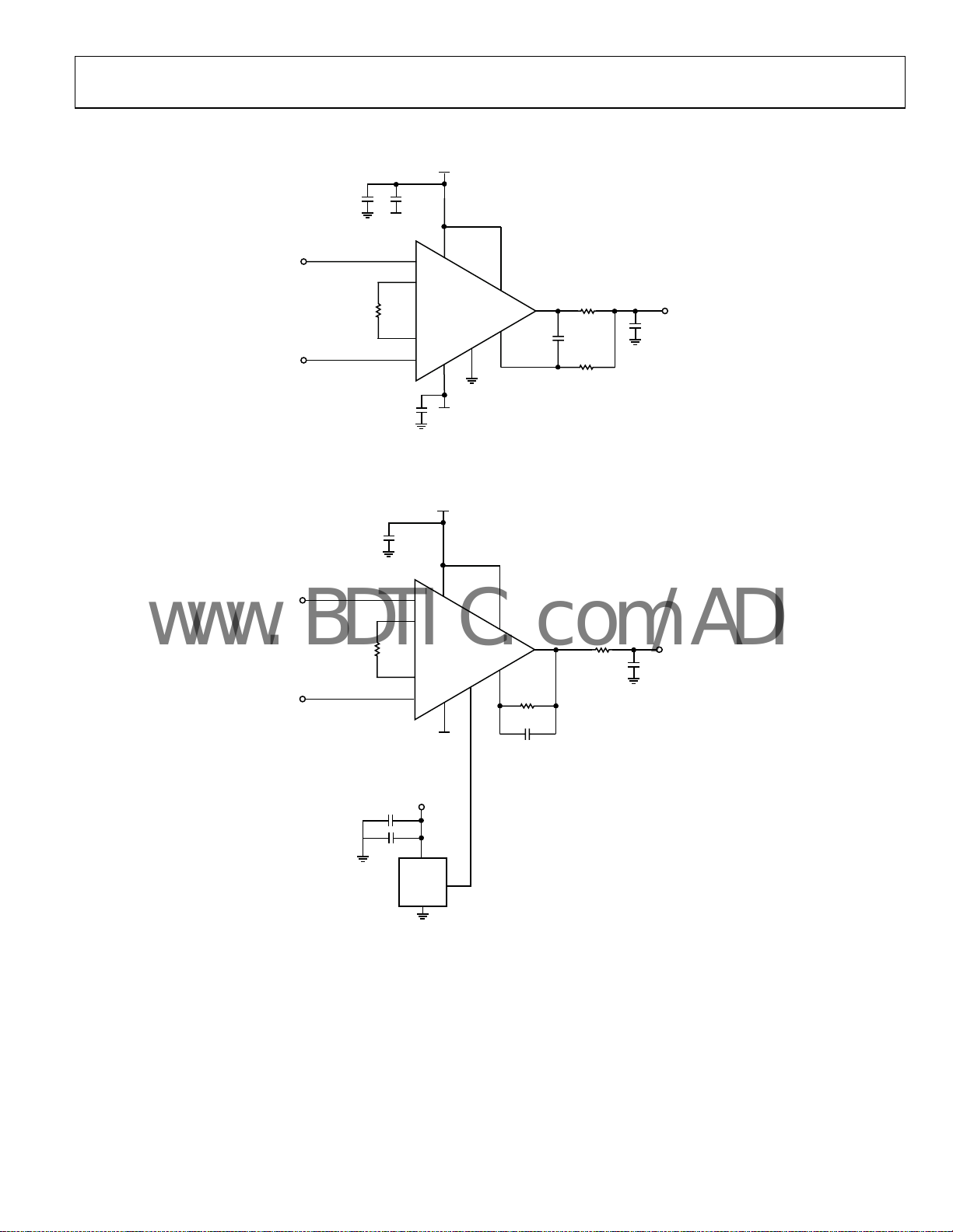
CIRCUIT DIAGRAMS/CONNECTIONS
S+
0.1µF
GND
3
V
IN+
R1
V
IN–
2
+
1
AD8553
10
–
8
9
GND
100kΩ
100kΩ
V
S+
6
4
5
7
R2
C2
0.1µF
R3
100Ω
R3 AND C3 VALUES ARE
RECOMMENDED T O DRIVE
AN A/D CONVERTER
GND
C3
1µF
V
OUT
GND
05474-032
Figure 31. Single-Supply Connection Diagram Using Voltage Divider Reference
S+
0.1µF
GND
V
IN+
V
IN–
0.1µF
V
S–
2
3
+
1
R1
0.1µF
AD8553
10
–
8
9
VS–
GND
6
4
5
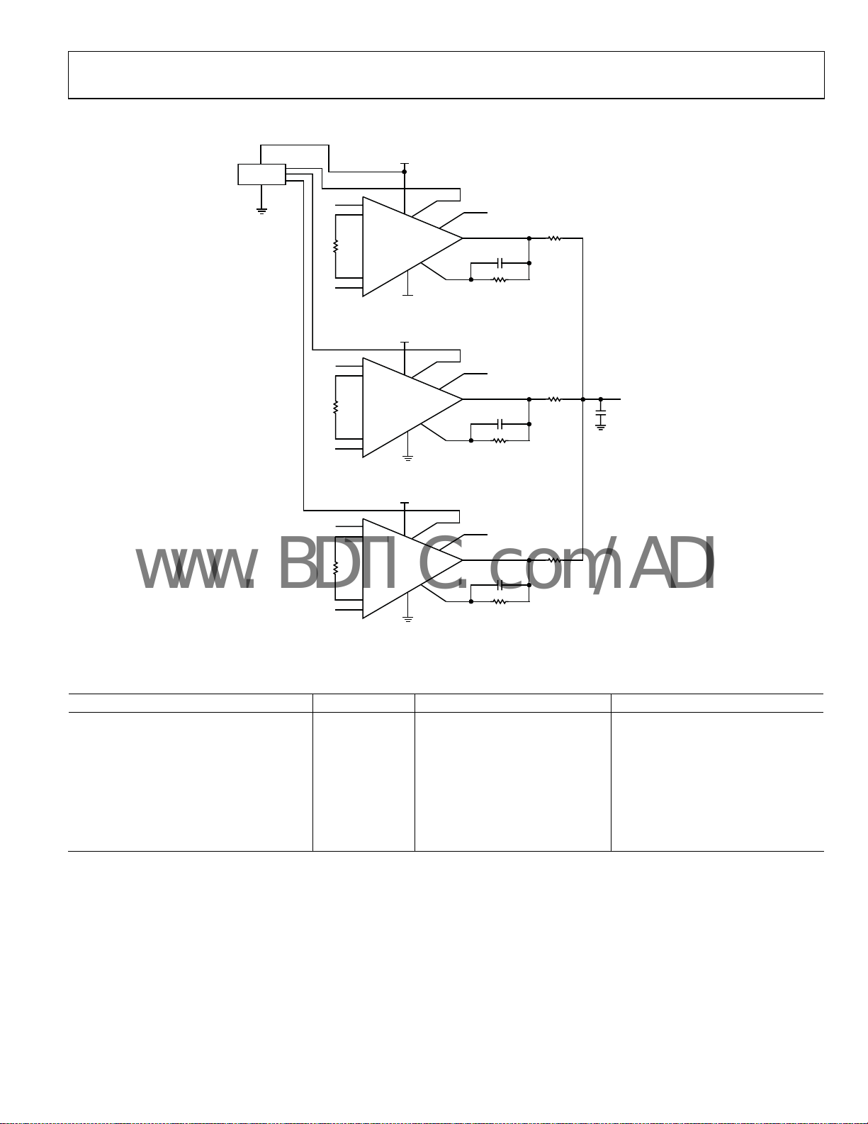
7
R2
C2
R3
100Ω
R3 AND C3 VALUES ARE
RECOMMENDED T O DRIVE
AN A/D CONVERTER
GND
C3
1µF
V
OUT
05474-031
Figure 32. Dual-Supply Connection Diagram
Rev. 0 | Page 14 of 20
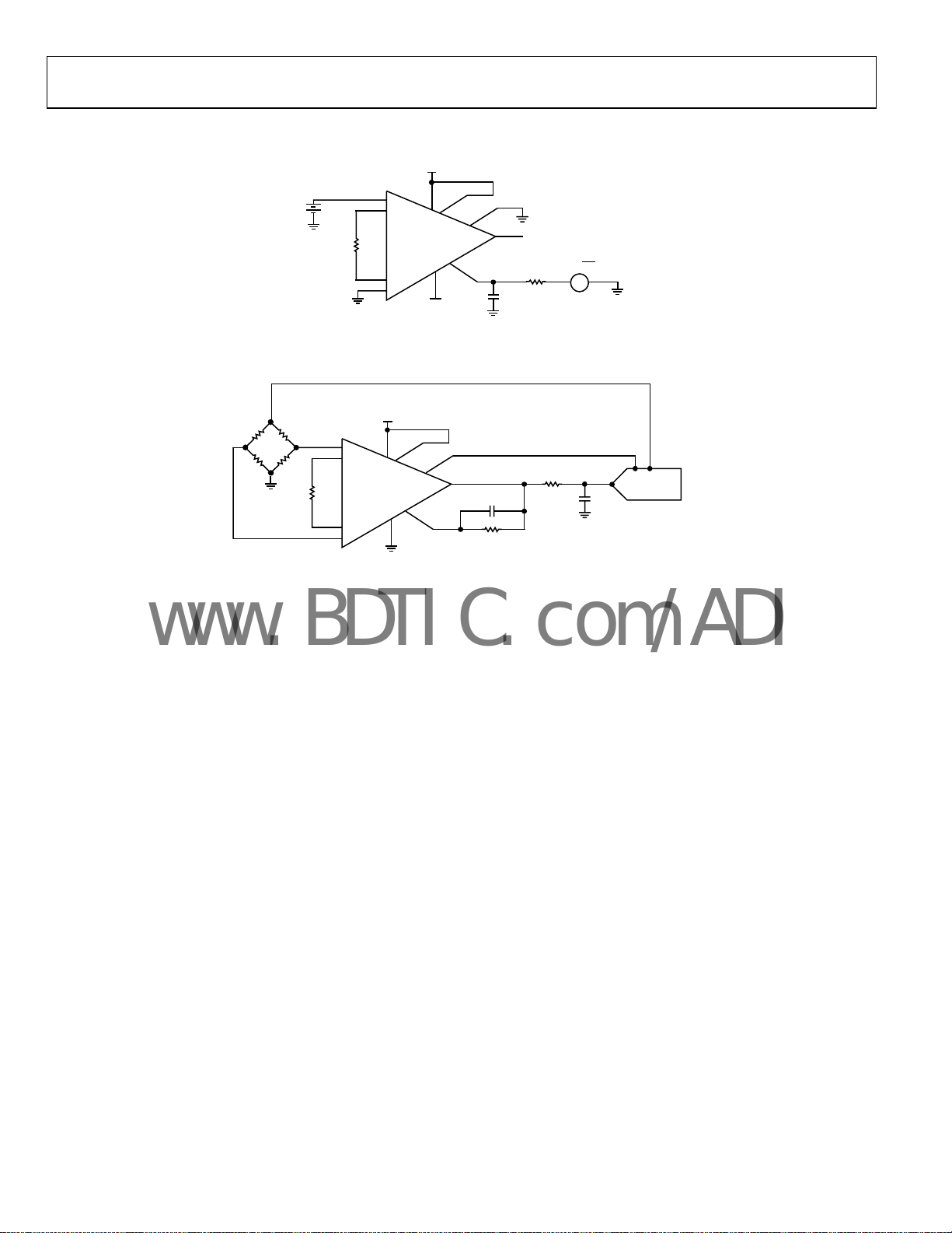
AD8553
V
V
www.BDTIC.com/ADI
S+
0.1µF
GND
V
IN+
V
IN–
Figure 33. Dual-Supply Connection Diagram with
0.1µF
V
S–
3
2
+
GND
6
5
7
R3
100Ω
4
C2
GND
R2
R3 AND C3 VALUES ARE
RECOMMENDED T O DRIVE
AN A/D CONVERTER
C3
1µF
V
OUT
05474-034
1
R1
0.1µF
10
9
GND
–
AD8553
8
VS–
Low Impedance Output
S+
0.1µF
GND
2
V
IN+
R1
V
IN–
3
+
1
AD8553
10
–
9
8
V
S–
6
4
5
7
R2
C2
R3
100Ω
R3 AND C3 VALUES ARE
RECOMMENDED T O DRIVE
AN A/D CONVERTER
GND
C3
1µF
V
OUT
V
CC
1.0µF
0.1µF
V
IN
V
OUT
GND
Figure 34. Dual-Supply Connection Diagram Using IC Voltage Reference
Rev. 0 | Page 15 of 20
05474-035
AD8553
V
V
www.BDTIC.com/ADI
S+
2
IN
1
R1
10
9
+
AD8553
_
3
8
V
S–
Figure 35. Voltage-to-Current Converter, 0 μA to 30 μA Source
V
S+
2
3
+
1
AD8553
R1
10
9
_
Figure 36. Example of an AD8553 Driving a Converter at V
7
5
8
6
7
4
NC (NO CONNECT )
V
IN
5
0.1µF
6
4
V
REF
C2
R2
10kΩ
= 2.5V
AMMETER
100Ω
IO=
A
R1
S+
1µF
= 5 V
05474-037
A/D
A/D
CONVERTER
05474-038
Rev. 0 | Page 16 of 20
AD8553
www.BDTIC.com/ADI
V
S+
LOGIC
2
3
+
1
AD8553
R1
10
9
2
1
R6
10
9
_
+
AD8553
_
8
V
S–
V
S+
3
8
6
V
7
5
6
7
5
REF
4
C2
R2
V
REF
4
C3
R7
R3
100Ω
R8
100Ω
1µF
V
OUT
V
S+
6
V
7
5
REF
4
C4
R12
R13
100Ω
05474-039
R11
10
2
1
9
+
AD8553
_
3
8
Figure 37. Multiplexed Output
Table 5. Recommended External Component Values for Selected Gains
Desired Gain (V/V) R1 (Ω) R2 || C2 (Ω || F) Calculated Gain
1 200 k 100 k || 1200p 1
2 100 k 100 k || 1200p 2
5 40.2 k 100 k || 1200p
10 20 k 100 k || 1200p
50 4.02 k 100 k || 1200p
100 3.92 k 196 k || 560p
500 3.92 k 976 k || 120p
4.975
10
49.75
100
497.95
1000 3.92 k 1.96 M || 56p 1000
Rev. 0 | Page 17 of 20
AD8553
www.BDTIC.com/ADI
OUTLINE DIMENSIONS
3.10
3.00
2.90
6
10
3.10
3.00
2.90
1
PIN 1
0.50 BSC
0.95
0.85
0.75
0.15
0.05
0.33
0.17
COPLANARITY
0.10
COMPLIANT TO JEDEC STANDARDS MO-187-BA
Figure 38. 10-Lead Mini Small Outline Package [MSOP]
5.15
4.90
4.65
5
1.10 MAX
SEATING
PLANE
(R
M-10)
0.23
0.08
8°
0°
Dimensions shown in millimeters
0.80
0.60
0.40
ORDERING GUIDE
Model Temperature Range Package Description Package Option Branding
AD8553ARMZ-R2
AD8553ARMZ-REEL
1
Z = Pb-free part.
1
1
−40°C to +85°C 10-Lead MSOP RM-10 A09
−40°C to +85°C 10-Lead MSOP RM-10 A09
Rev. 0 | Page 18 of 20

AD8553
www.BDTIC.com/ADI
NOTES
Rev. 0 | Page 19 of 20

AD8553
www.BDTIC.com/ADI
NOTES
©2005 Analog Devices, Inc. All rights reserved. Trademarks and
registered trademarks are the property of their respective owners.
D05474-0-10/05(0)
Rev. 0 | Page 20 of 20
 Loading...