

General-Purpose CMOS
NC
–IN A
+IN A
V–
V+
OUT A
NC
NC
1
2
3
4
8
7
6
5
AD8541
NC = NO CONNECT
AD8542
1
2
3
4
8
7
6
5
OUT A
–IN A
+IN A
V–
+IN B
–IN B
OUT B
V+
a
FEATURES
Single-Supply Operation: 2.7 V to 5.5 V
Low Supply Current: 45 A/Amplifier
Wide Bandwidth: 1 MHz
No Phase Reversal
Low Input Currents: 4 pA
Unity Gain Stable
Rail-to-Rail Input and Output
APPLICATIONS
ASIC Input or Output Amplifier
Sensor Interface
Piezo Electric Transducer Amplifier
Medical Instrumentation
Mobile Communication
Audio Output
Portable Systems
GENERAL DESCRIPTION
The AD8541/AD8542/AD8544 are single, dual, and quad railto-rail input and output single-supply amplifiers featuring very
low supply current and 1 MHz bandwidth. All are guaranteed to
operate from a 2.7 V single supply as well as a 5 V supply. These
parts provide 1 MHz bandwidth at a low current consumption
of 45 mA per amplifier.
Very low input bias currents enable the AD8541/AD8542/AD8544
to be used for integrators, photodiode amplifiers, piezo electric
sensors, and other applications with high source impedance. Supply current is only 45 mA per amplifier, ideal for battery operation.
Rail-to-rail inputs and outputs are useful to designers buffering
ASICs in single-supply systems. The AD8541/AD8542/AD8544
are optimized to maintain high gains at lower supply voltages,
making them useful for active filters and gain stages.
The AD8541/AD8542/AD8544 are specified over the extended
industrial temperature range (–40∞C to +125∞C). The AD8541
is available in 8-lead SOIC, 5-lead SC70, and 5-lead SOT-23
packages. The AD8542 is available in 8-lead SOIC, 8-lead
MSOP, and 8-lead TSSOP surface-mount packages. The AD8544
is available in 14-lead narrow SOIC and 14-lead TSSOP surfacemount packages. All MSOP, SC70, and SOT versions are available
in tape and reel only.
Rail-to-Rail Amplifiers
AD8541/AD8542/AD8544
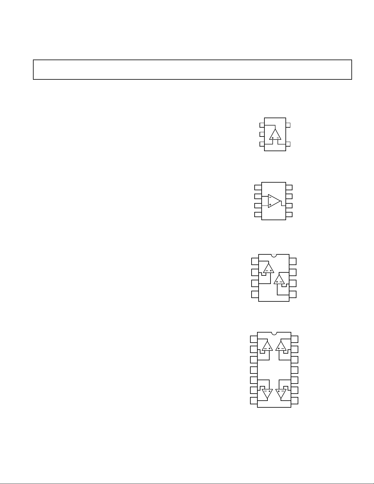
PIN CONFIGURATIONS
5-Lead SC70 and SOT-23
(KS and RT Suffixes)
+IN A
Vⴚ
AD8541
1
2
3
OUT A
8-Lead SOIC
(R Suffix)
8-Lead SOIC, MSOP, and TSSOP
(R, RM, and RU Suffixes)
14-Lead SOIC and TSSOP
(R and RU Suffixes)
1
OUT A
2
–IN A
3
+IN A
AD8544
4
V+
5
+IN B
6
–IN B
7
OUT B
5
4
V+
ⴚIN A
14
13
12
11
10
9
8
OUT D
–IN D
+IN D
V–
+IN C
–IN C
OUT C
REV. D
Information furnished by Analog Devices is believed to be accurate and
reliable. However, no responsibility is assumed by Analog Devices for its
use, nor for any infringements of patents or other rights of third parties that
may result from its use. No license is granted by implication or otherwise
under any patent or patent rights of Analog Devices. Trademarks and
registered trademarks are the property of their respective owners.
One Technology Way, P.O. Box 9106, Norwood, MA 02062-9106, U.S.A.
Tel: 781/329-4700 www.analog.com
Fax: 781/326-8703 © 2004 Analog Devices, Inc. All rights reserved.

AD8541/AD8542/AD8544–SPECIFICATIONS
ELECTRICAL CHARACTERISTICS
(VS = 2.7 V, VCM = 1.35 V, TA = 25ⴗC, unless otherwise noted.)
Parameter Symbol Conditions Min Typ Max Unit
INPUT CHARACTERISTICS
Offset Voltage V
Input Bias Current I
Input Offset Current I
B
OS
OS
–40∞C £ T
–40∞C £ T
–40∞C £ T
–40∞C £ T
–40∞C £ T
£ +125∞C7mV
A
£ +85∞C 100 pA
A
£ +125∞C 1,000 pA
A
£ +85∞C50pA
A
£ +125∞C 500 pA
A
16 mV
460 pA
0.1 30 pA
Input Voltage Range 0 2.7 V
Common-Mode Rejection Ratio CMRR V
Large Signal Voltage Gain A
Offset Voltage Drift DV
Bias Current Drift DI
VO
/DT –40∞C £ TA £ +125∞C4mV/∞C
OS
/DT –40∞C £ TA £ +85∞C 100 fA/∞C
B
= 0 V to 2.7 V 40 45 dB
CM
–40∞C £ T
£ +125∞C38 dB
A
RL = 100 kW , VO = 0.5 V to 2.2 V 100 500 V/mV
–40∞C £ T
–40∞C £ T
–40∞C £ T
£ +85∞C50 V/mV
A
£ +125∞C2 V/mV
A
£ +125∞C 2,000 fA/∞C
A
Offset Current Drift DIOS/DT –40∞C £ TA £ +125∞C25fA/∞C
OUTPUT CHARACTERISTICS
Output Voltage High V
Output Voltage Low V
Output Current I
Closed-Loop Output Impedance Z
OUT
± I
OH
OL
SC
OUT
IL = 1 mA 2.575 2.65 V
–40∞C £ T
£ +125∞C 2.550 V
A
IL = 1 mA 35 100 mV
–40∞C £ T
V
OUT
£ +125∞C 125 mV
A
= VS – 1 V 15 mA
± 20 mA
f = 200 kHz, AV = 1 50 W
POWER SUPPLY
Power Supply Rejection Ratio PSRR VS = 2.5 V to 6 V 65 76 dB
£ +125∞C60 dB
A
Supply Current/Amplifier I
SY
–40∞C £ T
VO = 0 V 38 55 mA
–40∞C £ TA £ +125∞C75mA
DYNAMIC PERFORMANCE
Slew Rate SR RL = 100 kW 0.4 0.75 V/ms
Settling Time t
S
To 0.1% (1 V Step) 5 ms
Gain Bandwidth Product GBP 980 kHz
Phase Margin Fo63Degrees
NOISE PERFORMANCE
Voltage Noise Density e
Current Noise Density i
Specifications subject to change without notice.
n
e
n
n
f = 1 kHz 40 nV/÷Hz
f = 10 kHz 38 nV/÷Hz
<0.1 pA/÷Hz
–2–
REV. D

AD8541/AD8542/AD8544
ELECTRICAL CHARACTERISTICS
(VS = 3.0 V, VCM = 1.5 V, TA = 25ⴗC, unless otherwise noted.)
Parameter Symbol Conditions Min Typ Max Unit
INPUT CHARACTERISTICS
Offset Voltage V
Input Bias Current I
Input Offset Current I
B
OS
OS
–40∞C £ T
–40∞C £ T
–40∞C £ T
–40∞C £ T
–40∞C £ T
£ +125∞C7mV
A
£ +85∞C 100 pA
A
£ +125∞C 1,000 pA
A
£ +85∞C50pA
A
£ +125∞C 500 pA
A
16 mV
460 pA
0.1 30 pA
Input Voltage Range 03V
Common-Mode Rejection Ratio CMRR V
Large Signal Voltage Gain A
Offset Voltage Drift DV
Bias Current Drift DI
VO
/DT –40∞C £ TA £ +125∞C4mV/∞C
OS
/DT –40∞C £ TA £ +85∞C 100 fA/∞C
B
= 0 V to 3 V 40 45 dB
CM
–40∞C £ T
£ +125∞C38 dB
A
RL = 100 kW , VO = 0.5 V to 2.2 V 100 500 V/mV
–40∞C £ T
–40∞C £ T
–40∞C £ T
£ +85∞C50 V/mV
A
£ +125∞C2 V/mV
A
£ +125∞C 2,000 fA/∞C
A
Offset Current Drift DIOS/DT –40∞C £ TA £ +125∞C25fA/∞C
OUTPUT CHARACTERISTICS
Output Voltage High V
Output Voltage Low V
Output Current I
Closed-Loop Output Impedance Z
± I
OH
OL
OUT
SC
OUT
IL = 1 mA 2.875 2.955 V
–40∞C £ T
£ +125∞C 2.850 V
A
IL = 1 mA 32 100 mV
–40∞C £ T
V
OUT
£ +125∞C 125 mV
A
= VS – 1 V 18 mA
± 25 mA
f = 200 kHz, AV = 1 50 W
POWER SUPPLY
Power Supply Rejection Ratio PSRR VS = 2.5 V to 6 V 65 76 dB
£ +125∞C60 dB
A
Supply Current/Amplifier I
SY
–40∞C £ T
VO = 0 V 40 60 mA
–40∞C £ TA £ +125∞C75mA
DYNAMIC PERFORMANCE
Slew Rate SR R
Settling Time t
S
= 100 kW 0.4 0.8 V/ms
L
To 0.01% (1 V Step) 5 ms
Gain Bandwidth Product GBP 980 kHz
Phase Margin Fo64Degrees
NOISE PERFORMANCE
Voltage Noise Density e
Current Noise Density i
Specifications subject to change without notice.
n
e
n
n
f = 1 kHz 42 nV/÷Hz
f = 10 kHz 38 nV/÷Hz
<0.1 pA/÷Hz
REV. D
–3–

AD8541/AD8542/AD8544–SPECIFICATIONS
ELECTRICAL CHARACTERISTICS
(VS = 5.0 V, VCM = 2.5 V, TA = 25ⴗC, unless otherwise noted.)
Parameter Symbol Conditions Min Typ Max Unit
INPUT CHARACTERISTICS
Offset Voltage V
Input Bias Current I
Input Offset Current I
B
OS
OS
–40∞C £ T
–40∞C £ T
–40∞C £ T
–40∞C £ T
–40∞C £ T
£ +125∞C7mV
A
£ +85∞C 100 pA
A
£ +125∞C 1,000 pA
A
£ +85∞C50pA
A
£ +125∞C 500 pA
A
16 mV
460 pA
0.1 30 pA
Input Voltage Range 0 5V
Common-Mode Rejection Ratio CMRR V
Large Signal Voltage Gain A
Offset Voltage Drift DV
Bias Current Drift DI
VO
/DT –40∞C £ TA £ +125∞C4mV/∞C
OS
/DT –40∞C £ TA £ +85∞C 100 fA/∞C
B
= 0 V to 5 V 40 48 dB
CM
–40∞C £ T
£ +125∞C38 dB
A
RL = 100 kW , VO = 0.5 V to 2.2 V 20 40 V/mV
–40∞C £ T
–40∞C £ T
–40∞C £ T
£ +85∞C10 V/mV
A
£ +125∞C2 V/mV
A
£ +125∞C 2,000 fA/∞C
A
Offset Current Drift DIOS/DT –40∞C £ TA £ +125∞C25fA/∞C
OUTPUT CHARACTERISTICS
Output Voltage High V
Output Voltage Low V
Output Current I
Closed-Loop Output Impedance Z
OUT
± I
OH
OL
SC
OUT
IL = 1 mA 4.9 4.965 V
–40∞C £ T
£ +125∞C 4.875 V
A
IL = 1 mA 25 100 mV
–40∞C £ T
V
OUT
£ +125∞C 125 mV
A
= VS – 1 V 30 mA
± 60 mA
f = 200 kHz, AV = 1 45 W
POWER SUPPLY
Power Supply Rejection Ratio PSRR VS = 2.5 V to 6 V 65 76 dB
£ +125∞C60 dB
A
Supply Current/Amplifier I
SY
–40∞C £ T
VO = 0 V 45 65 mA
–40∞C £ TA £ +125∞C85mA
DYNAMIC PERFORMANCE
Slew Rate SR RL = 100 kW, CL = 200 pF 0.45 0.92 V/ms
Full-Power Bandwidth BW
Settling Time t
S
P
1% Distortion 70 kHz
To 0.1% (1 V Step) 6 ms
Gain Bandwidth Product GBP 1,000 kHz
Phase Margin Fo67Degrees
NOISE PERFORMANCE
Voltage Noise Density e
Current Noise Density i
Specifications subject to change without notice.
n
e
n
n
f = 1 kHz 42 nV/÷Hz
f = 10 kHz 38 nV/÷Hz
<0.1 pA/÷Hz
–4–
REV. D
AD8541/AD8542/AD8544
ABSOLUTE MAXIMUM RATINGS
1
PACKAGE INFORMATION
Supply Voltage (VS) . . . . . . . . . . . . . . . . . . . . . . . . . . . . . . 6 V
Input Voltage . . . . . . . . . . . . . . . . . . . . . . . . . . . . GND to V
Differential Input Voltage2 . . . . . . . . . . . . . . . . . . . . . . . ± 6 V
Storage Temperature Range . . . . . . . . . . . . –65∞C to +150∞C
Operating Temperature Range . . . . . . . . . . –40∞C to +125∞C
Junction Temperature Range . . . . . . . . . . . . –65∞C to +150∞C
Lead Temperature Range (Soldering, 60 sec) . . . . . . . 300∞C
NOTES
1
Stresses above those listed under Absolute Maximum Ratings may cause permanent damage to the device. This is a stress rating only; functional operation of the
device at these or any other conditions above those listed in the operational
sections of this specification is not implied. Exposure to absolute maximum rating
conditions for extended periods may affect device reliability.
2
For supplies less than 6 V, the differential input voltage is equal to ±VS.
ORDERING GUIDE
Package Type JA*
S
5-Lead SC70 (KS) 376 126 ∞C/W
5-Lead SOT-23 (RT) 230 146 ∞C/W
8-Lead SOIC (R) 158 43 ∞C/W
8-Lead MSOP (RM) 210 45 ∞C/W
8-Lead TSSOP (RU) 240 43 ∞C/W
14-Lead SOIC (R) 120 36 ∞C/W
14-Lead TSSOP (RU) 240 43 ∞C/W
*qJA is specified for worst-case conditions, i.e.,
onto a circuit board for surface mount packages.
Temperature Package Package Branding
Model Range Description Option Information
AD8541AKS-R2 –40∞C to +125∞C 5-Lead SC70 KS-5 A4B
AD8541AKS-REEL7 –40∞C to +125∞C 5-Lead SC70 KS-5 A4B
AD8541AKSZ-REEL7* –40∞C to +125∞C 5-Lead SC70 KS-5 A4B
AD8541AR –40∞C to +125∞C 8-Lead SOIC R-8
AD8541AR-REEL –40∞C to +125∞C 8-Lead SOIC R-8
AD8541AR-REEL7 –40∞C to +125∞C 8-Lead SOIC R-8
AD8541ART-R2 –40∞C to +125∞C 5-Lead SOT-23 RT-5 A4A
AD8541ART-REEL –40∞C to +125∞C 5-Lead SOT-23 RT-5 A4A
AD8541ART-REEL7 –40∞C to +125∞C 5-Lead SOT-23 RT-5 A4A
AD8541ARTZ-REEL* –40∞C to +125∞C 5-Lead SOT-23 RT-5 A4A
AD8541ARTZ-REEL7* –40∞C to +125∞C 5-Lead SOT-23 RT-5 A4A
AD8542AR –40∞C to +125∞C 8-Lead SOIC R-8
AD8542AR-REEL –40∞C to +125∞C 8-Lead SOIC R-8
AD8542AR-REEL7 –40∞C to +125∞C 8-Lead SOIC R-8
AD8542ARZ* –40∞C to +125∞C 8-Lead SOIC R-8
AD8542ARZ-REEL* –40∞C to +125∞C 8-Lead SOIC R-8
AD8542ARZ-REEL7* –40∞C to +125∞C 8-Lead SOIC R-8
AD8542ARM-R2 –40∞C to +125∞C 8-Lead MSOP RM-8 AVA
AD8542ARM-REEL –40∞C to +125∞C 8-Lead MSOP RM-8 AVA
AD8542ARU –40∞C to +125∞C 8-Lead TSSOP RU-8
AD8542ARU-REEL –40∞C to +125∞C 8-Lead TSSOP RU-8
AD8542ARUZ* –40∞C to +125∞C 8-Lead TSSOP RU-8
AD8542ARUZ-REEL* –40∞C to +125∞C 8-Lead TSSOP RU-8
AD8544AR –40∞C to +125∞C 14-Lead SOIC R-14
AD8544AR-REEL –40∞C to +125∞C 14-Lead SOIC R-14
AD8544AR-REEL7 –40∞C to +125∞C 14-Lead SOIC R-14
AD8544ARZ* –40∞C to +125∞C 14-Lead SOIC R-14
AD8544ARZ-REEL* –40∞C to +125∞C 14-Lead SOIC R-14
AD8544ARZ-REEL7* –40∞C to +125∞C 14-Lead SOIC R-14
AD8544ARU –40∞C to +125∞C 14-Lead TSSOP RU-14
AD8544ARU-REEL –40∞C to +125∞C 14-Lead TSSOP RU-14
AD8544ARUZ* –40∞C to +125∞C 14-Lead TSSOP RU-14
AD8544ARUZ-REEL* –40∞C to +125∞C 14-Lead TSSOP RU-14
*Z = Pb-free part.
ESD CAUTION
ESD (electrostatic discharge) sensitive device. Electrostatic charges as high as 4000 V readily
accumulate on the human body and test equipment and can discharge without detection. Although
the AD8541/AD8542/AD8544 feature proprietary ESD protection circuitry, permanent damage
may occur on devices subjected to high energy electrostatic discharges. Therefore, proper ESD
precautions are recommended to avoid performance degradation or loss of functionality.
JC
is specified for device soldered
JA
WARNING!
ESD SENSITIVE DEVICE
Unit
REV. D
–5–

AD8541/AD8542/AD8544
–Typical Performance Characteristics
180
160
140
120
100
80
60
NUMBER OF AMPLIFIERS
40
20
0
ⴚ4.5 ⴚ3.5
ⴚ2.5 ⴚ1.5
INPUT OFFSET VOLTAGE – mV
ⴚ0.5 1.5 2.5 3.50.5
VS = 5V
V
T
TPC 1. Input Offset Voltage
Distribution
400
VS = 2.7V AND 5V
= VS/2
V
CM
350
300
250
200
150
100
INPUT BIAS CURRENT – pA
50
0
ⴚ40 ⴚ20
02040 80100 12060
TEMPERATURE – ⴗC
TPC 4. Input Bias Current vs.
Temperature
= 2.5V
CM
= 25ⴗC
A
140
4.5
1.0
VS = 2.7V AND 5V
0.5
= VS/2
V
CM
0.0
ⴚ0.5
ⴚ1.0
ⴚ1.5
ⴚ2.0
ⴚ2.5
ⴚ3.0
INPUT OFFSET VOLTAGE – mV
ⴚ3.5
ⴚ4.0
ⴚ55 ⴚ35
ⴚ15
525456585105 125
TEMPERATURE – ⴗC
TPC 2. Input Offset Voltage
vs. Temperature
7
VS = 2.7V AND 5V
= VS/2
V
CM
6
5
4
3
2
1
INPUT OFFSET CURRENT – pA
0
ⴚ1
ⴚ15
ⴚ55 ⴚ35
545
25 85 105 12565
TEMPERATURE – ⴗC
TPC 5. Input Offset Current vs.
Temperature
145
145
9
VS = 2.7V AND 5V
= VS/2
V
CM
8
7
6
5
4
3
2
INPUT BIAS CURRENT – pA
1
0
ⴚ0.5
0.5 5.5
1.5 2.5 3.5 4.5
COMMON-MODE VOLTAGE – V
TPC 3. Input Bias Current vs.
Common-Mode Voltage
160
VS = 2.7V
140
= 25ⴗC
T
A
120
100
POWER SUPPLY REJECTION – dB
ⴚ20
ⴚ40
80
60
40
20
ⴚPSRR
+PSRR
0
100 1k 10M10k 100k 1M
FREQUENCY – Hz
TPC 6. Power Supply Rejection
Ratio vs. Frequency
10k
VS = 2.7V
= 25ⴗC
T
A
1k
100
10
1
⌬ OUTPUT VOLTAGE – mV
0.1
0.01
0.001 0.01 100
SOURCE
SINK
0.1 1 10
LOAD CURRENT – mA
TPC 7. Output Voltage to Supply
Rail vs. Load Current
3.0
2.5
2.0
1.5
1.0
OUTPUT SWING – V p-p
0.5
0
1k 10k 10M
FREQUENCY – Hz
VS = 2.7V
V
IN
= 2k⍀
R
L
= 25ⴗC
T
A
100k 1M
= 2.5V p-p
TPC 8. Closed-Loop Output
Voltage Swing vs. Frequency
–6–
60
VS = 2.7V
50
=
R
L
= 25ⴗC
T
A
40
+OS
30
20
10
SMALL SIGNAL OVERSHOOT – %
0
10 100 10k
CAPACITANCE – pF
ⴚOS
1k
TPC 9. Small Signal Overshoot vs.
Load Capacitance
REV. D

AD8541/AD8542/AD8544
FREQUENCY – Hz
OUTPUT SWING – V p-p
3.0
2.5
0
1k 10k 10M
100k 1M
2.0
1.5
0.5
1.0
VS = 5V
V
IN
= 4.9V p-p
R
L
= NO LOAD
T
A
= 25ⴗC
4.0
3.5
5.0
4.5
60
VS = 2.7V
= 10k⍀
R
50
L
= 25ⴗC
T
A
40
+OS
30
20
10
SMALL SIGNAL OVERSHOOT – %
0
10 100 10k
CAPACITANCE – pF
ⴚOS
1k
TPC 10. Small Signal Overshoot vs.
Load Capacitance
1.35V
VS = 2.7V
= 2k⍀
R
L
= 1
A
V
= 25ⴗC
T
A
500mV
10s
TPC 13. Large Signal Transient
Response
60
VS = 2.7V
50
= 2k⍀
R
L
= 25ⴗC
T
A
40
30
20
10
SMALL SIGNAL OVERSHOOT – %
0
10 100 10k
CAPACITANCE – pF
+OS
ⴚOS
1k
TPC 11. Small Signal Overshoot
vs. Load Capacitance
VS = 2.7V
= NO LOAD
R
L
= 25ⴗC
T
A
80
60
40
20
GAIN – dB
0
1k 10k 10M100k 1M
FREQUENCY – Hz
TPC 14. Open-Loop Gain and
Phase vs. Frequency
1.35V
TPC 12. Small Signal Transient
Response
160
140
120
45
90
135
180
100
PHASE SHIFT – Degrees
ⴚ20
POWER SUPPLY REJECTION RATIO – dB
ⴚ40
TPC 15. Power Supply Rejection
Ratio vs. Frequency
VS = 2.7V
= 100kV
R
L
= 300pF
C
L
= 1
A
V
= 25 C
T
A
50mV
VS = 5V
= 25ⴗC
T
A
80
ⴚPSRR
60
+PSRR
40
20
0
100 1k 10M10k 100k 1M
FREQUENCY – Hz
10s
90
VS = 5V
80
= 25ⴗC
T
A
70
60
50
40
30
20
10
COMMON-MODE REJECTION – dB
0
ⴚ10
1k 10k 10M100k 1M
FREQUENCY – Hz
TPC 16. Common-Mode Rejection
Ratio vs. Frequency
REV. D
10k
VS = 5V
= 25ⴗC
T
A
1k
100
10
1
⌬ OUTPUT VOLTAGE – mV
0.1
0.01
0.001 0.01 100
SOURCE
SINK
0.1 1 10
LOAD CURRENT – mA
TPC 17. Output Voltage to Supply
Rail vs. Frequency
–7–
TPC 18. Closed-Loop Output
Voltage Swing vs. Frequency

AD8541/AD8542/AD8544
CAPACITANCE – pF
SMALL SIGNAL OVERSHOOT – %
60
0
10 100 10k
1k
30
20
10
40
VS = 5V
R
L
= 2k⍀
T
A
= 25ⴗC
50
+OS
ⴚOS
g
5.0
4.5
4.0
3.5
3.0
2.5
2.0
1.5
OUTPUT SWING – V p-p
1.0
0.5
0
1k 10k 10M
FREQUENCY – Hz
VS = 5V
= 4.9V p-p
V
IN
= 2k⍀
R
L
= 25ⴗC
T
A
100k 1M
TPC 19. Closed-Loop Output
Voltage Swing vs. Frequency
60
VS = 5V
50
=
R
L
= 25ⴗC
T
A
40
+OS
30
20
10
SMALL SIGNAL OVERSHOOT – %
0
10 100 10k
CAPACITANCE – pF
ⴚOS
1k
TPC 22. Small Signal Overshoot vs.
Load Capacitance
60
VS = 5V
50
= 10k⍀
R
L
= 25ⴗC
T
A
40
+OS
30
20
10
SMALL SIGNAL OVERSHOOT – %
0
10 100 10k
CAPACITANCE – pF
ⴚOS
1k
TPC 20. Small Signal Overshoot vs.
Load Capacitance
VS = 5V
= 100k⍀
R
L
= 300pF
C
L
= 1
A
V
= 25ⴗC
T
A
2.5V
50mV
10s
TPC 23. Small Signal Transient
Response
TPC 21. Small Signal Overshoot vs.
Load Capacitance
2.5V
VS = 5V
= 2k⍀
R
L
= 1
A
V
= 25ⴗC
T
A
1V
10s
TPC 24. Large Signal Transient
Response
VS = 5V
= NO LOAD
R
L
= 25ⴗC
T
A
80
60
40
20
GAIN – dB
0
1k 10k 10M100k 1M
FREQUENCY – Hz
TPC 25. Open-Loop Gain and Phase
vs. Frequency
60
TA = 25ⴗC
50
40
30
20
10
SUPPLY CURRENT/AMPLIFIER – A
0
01 6
23 45
SUPPLY VOLTAGE – V
TPC 27. Supply Current per
45
rees
90
135
180
PHASE SHIFT – De
V
IN
V
OUT
2.5V
1V
TPC 26. No Phase Reversal
VS = 5V
= 10k⍀
R
L
= 1
A
V
= 25ⴗC
T
A
20s
Amplifier vs. Supply Voltage
–8–
REV. D

AD8541/AD8542/AD8544
55
50
45
40
35
30
25
SUPPLY CURRENT/AMPLIFIER – A
20
ⴚ55 ⴚ35
VS = 5V
VS = 2.7V
ⴚ15
525456585105 125
TEMPERATURE – ⴗC
TPC 28. Supply Current per
Amplifier vs. Temperature
145
1,000
VS = 2.7V AND 5V
900
= 1
A
V
= 25ⴗC
T
800
A
700
600
500
400
300
IMPEDANCE – ⍀
200
100
0
1k 10k 100M100k 1M 10M
FREQUENCY – Hz
TPC 29. Closed-Loop Output
Impedance vs. Frequency
NOTES ON THE AD854x AMPLIFIERS
The AD8541/AD8542/AD8544 amplifiers are improved performance general-purpose operational amplifiers. Performance has
been improved over previous amplifiers in several ways.
Lower Supply Current for 1 MHz Gain Bandwidth
The AD854x series typically uses 45 mA of current per amplifier.
This is much less than the 200 mA to 700 mA used in earlier
generation parts with similar performance. This makes the
AD854x series a good choice for upgrading portable designs for
longer battery life. Alternatively, additional functions and performance can be added at the same current drain.
Higher Output Current
At 5 V single supply, the short-circuit current is typically 60 mA.
Even 1 V from the supply rail, the AD854x amplifiers can provide
30 mA, sourcing or sinking.
Sourcing and sinking are strong at lower voltages, with 15 mA
available at 2.7 V and 18 mA at 3.0 V. For even higher output
currents, please see the Analog Devices AD8531/AD8532/AD8534
parts, with output currents to 250 mA. Information on these
parts is available from your Analog Devices representative,
and data sheets are available at the Analog Devices website at
www.analog.com.
Better Performance at Lower Voltages
The AD854x family of parts has been designed to provide better
ac performance, at 3.0 V and 2.7 V, than previously available
parts. Typical gain-bandwidth product is close to 1 MHz at 2.7 V.
Voltage gain at 2.7 V and 3.0 V is typically 500,000. Phase margin
is typically over 60∞C, making the part easy to use.
APPLICATIONS
Notch Filter
The AD8542 has very high open-loop gain (especially with a
supply voltage below 4 V), which makes it useful for active filters
of all types. For example, Figure 1 illustrates the AD8542 in the
classic Twin-T Notch Filter design. The Twin-T Notch is desired
for simplicity, low output impedance, and minimal use of op
amps. In fact, this notch filter may be designed with only one op
amp if Q adjustment is not required. Simply remove U2 as illustrated in Figure 2. However, a major drawback to this circuit
topology is ensuring that all the Rs and Cs closely match. The
components must closely match or notch frequency offset and
VS = 5V
= 1
A
V
MARKER SET @ 10kHz
MARKER READING: 37.6V/ Hz
= 25ⴗC
T
A
200mV/DIVISION
05 2510 15 20
FREQUENCY – kHz
TPC 30. Voltage Noise
drift will cause the circuit to no longer attenuate at the ideal
notch frequency. To achieve desired performance, 1% or
better component tolerances or special component screens
are usually required. One method to desensitize the circuitto-component mismatch is to increase R2 with respect to
R1, which lowers Q. A lower Q increases attenuation over a
wider frequency range but reduces attenuation at the peak
notch frequency.
5.0V
8
3
U1
2
7
U2
1/2 AD8542
1
4
5
6
2.5V
R2
2.5k⍀
R1
97.5k⍀
REF
V
OUT
2.5V
REF
1
f0 =
2pRC
f0 =
4
[ ]
R
100k⍀R100k⍀
C2
53.6F
C
26.7nF
1
R1
1 ⴚ
R1+R2
R/2
50k⍀
26.7nF
C
1/2 AD8542
Figure 1. 60 Hz Twin-T Notch Filter, Q = 10
5.0V
7
R R
V
IN
2.5V
REF
2C
R/2
C
C
AD8541
3
V
2
6
4
OUT
Figure 2. 60 Hz Twin-T Notch Filter, Q = • (Ideal)
Figure 3 shows another example of the AD8542 in a notch
filter circuit. The FNDR notch filter has fewer critical
matching requirements than the Twin-T Notch and for the
FNDR Q is directly proportional to a single resistor R1.
While matching component values is still important, it is also
REV. D
–9–

AD8541/AD8542/AD8544
much easier and/or less expensive to accomplish in the FNDR
circuit. For example, the Twin-T notch uses three capacitors
with two unique values, whereas the FNDR circuit uses only two
capacitors, which may be of the same value. U3 is simply a buffer
that is added to lower the output impedance of the circuit.
2.5V
REF
1/4 AD8544
f =
2p
L =
R2C2
1
LC1
R1
Q ADJUST
200⍀
C1
1F
C2
1F
6
7
U2
5
2.5V
R
2.61k⍀
R
2.61k⍀
R
2.61k⍀
R
2.61k⍀
REF
1/4 AD8544
9
U3
10
3
2
13
12
2.5V
REF
8
1/4 AD8544
4
1
U1
11
1/4 AD8544
14
U4
SPARE
V
OUT
NC
Figure 3. FNDR 60 Hz Notch Filter with Output Buffer
Comparator Function
A comparator function is a common application for a spare op
amp in a quad package. Figure 4 illustrates 1/4 of the AD8544
as a comparator in a standard overload detection application.
Unlike many op amps, the AD854x family can double as
comparators because this op amp family has rail-to-rail differential
input range, rail-to-rail output, and a great speed versus power
ratio. R2 is used to introduce hysteresis. The AD854x, when
used as comparators, have 5 ms propagation delay at 5 V and 5 ms
overload recovery time.
Photodiode Application
The AD854x family has very high impedance with input bias
current typically around 4 pA. This characteristic allows the
AD854x op amps to be used in photodiode applications and
other applications that require high input impedance. Note that
the AD854x has significant voltage offset, which can be removed
by capacitive coupling or software calibration.
Figure 5 illustrates a photodiode or current measurement
application. The feedback resistor is limited to 10 MW to avoid
excessive output offset. Also, note that a resistor is not needed
on the noninverting input to cancel bias current offset because
the bias current related output offset is not significant when
compared to the voltage offset contribution. For the best
performance follow the standard high impedance layout
techniques including:
∑ Shield the circuit.
∑ Clean the circuit board.
∑ Put a trace connected to the noninverting input around the
inverting input.
∑ Use separate analog and digital power supplies.
C
100pF
R
10M⍀
V+
7
2
6
3
4
AD8541
V
OUT
2.5V
OR
REF
D
2.5V
REF
Figure 5. High Input Impedance Application–Photodiode
Amplifier
R2
DC
1M⍀
1/4 AD8544
V
OUT
R1
1k⍀
V
IN
2.5V
REF
2.5V
Figure 4. AD854x Comparator Application–Overload Detector
–10–
REV. D

AD8541/AD8542/AD8544
* AD8542 SPICE Macro-model Typical Values
* 6/98, Ver. 1
* TAM / ADSC
*
* Copyright 1998 by Analog Devices
*
* Refer to “README.DOC” file for License
* Statement. Use of this model indicates your
* acceptance of the terms and provisions in
* the License Statement.
*
* Node Assignments
* noninverting input
*|inverting input
* || positive supply
* || | negative supply
* || | | output
* || | | |
* || | | |
.SUBCKT AD8542 1 2 99 50 45
*
* INPUT STAGE
*
M1 4 1 8 8 PIX L=0.6E-6 W=16E-6
M2 6 7 8 8 PIX L=0.6E-6 W=16E-6
M3 11 1 10 10 NIX L=0.6E-6 W=16E-6
M4 12 7 10 10 NIX L=0.6E-6 W=16E-6
RC1 4 50 20E3
RC2 6 50 20E3
RC3 99 11 20E3
RC4 99 12 20E3
C1 4 6 1.5E-12
C2 11 12 1.5E-12
I1 99 8 1E-5
I2 10 50 1E-5
V1 99 9 0.2
V2 13 50 0.2
D1 8 9 DX
D2 13 10 DX
EOS 7 2 POLY(3) (22,98) (73,98) (81,0) 1E-3 1 1 1
IOS 1 2 2.5E-12
*
* CMRR 64dB, ZERO AT 20kHz
*
ECM1 21 98 POLY(2) (1,98) (2,98) 0 .5 .5
RCM1 21 22 79.6E3
CCM1 21 22 100E-12
RCM2 22 98 50
*
* PSRR=90dB, ZERO AT 200Hz
*
RPS1 70 0 1E6
RPS2 71 0 1E6
CPS1 99 70 1E-5
CPS2 50 71 1E-5
EPSY 98 72 POLY(2) (70,0) (0,71) 0 1 1
RPS3 72 73 1.59E6
CPS3 72 73 500E-12
RPS4 73 98 25
*
* VOLTAGE NOISE REFERENCE OF 35nV/rt(Hz)
*
VN1 80 0 0
RN1 80 0 16.45E-3
HN 81 0 VN1 35
RN2 81 0 1
*
* INTERNAL VOLTAGE REFERENCE
*
VFIX 90 98 DC 1
S1 90 91 (50,99) VSY_SWITCH
VSN1 91 92 DC 0
RSY 92 98 1E3
EREF 98 0 POLY(2) (99,0) (50,0) 0 .5 .5
GSY 99 50 POLY(1) (99,50) 0 3.7E-6
*
* ADAPTIVE GAIN STAGE
* AT Vsy>+4.2, AVol=45 V/mv
* AT Vsy<+3.8, AVol=450 V/mv
*
G1 98 30 POLY(2) (4,6) (11,12) 0 2.5E-5 2.5E-5
VR1 30 31 DC 0
H1 31 98 POLY(2) VR1 VSN1 0 5.45E6 0 0 49.05E9
CF 45 30 10E-12
D3 30 99 DX
D4 50 30 DX
*
* OUTPUT STAGE
*
M5 45 46 99 99 POX L=0.6E-6 W=375E-6
M6 45 47 50 50 NOX L=0.6E-6 W=500E-6
EG1 99 46 POLY(1) (98,30) 1.05 1
EG2 47 50 POLY(1) (30,98) 1.04 1
*
* MODELS
*
.MODEL POX PMOS (LEVEL=2,KP=20E-6,VTO=-
+1,LAMBDA=0.067)
.MODEL NOX NMOS (LEVEL=2,KP=20E-
+6,VTO=1,LAMBDA=0.067)
.MODEL PIX PMOS (LEVEL=2,KP=20E-6,VTO=-
+0.7,LAMBDA=0.01,KF=1E-31)
.MODEL NIX NMOS (LEVEL=2,KP=20E-
+6,VTO=0.7,LAMBDA=0.01,KF=1E-31)
.MODEL DX D(IS=1E-14)
.MODEL VSY_SWITCH VSWITCH(ROFF=100E3,RON=1,VOFF=-
+4.2,VON=-3.5)
.ENDS AD8542
REV. D
–11–

AD8541/AD8542/AD8544
CONTROLLING DIMENSIONS ARE IN MILLIMETERS; INCH DIMENSIONS
(IN PARENTHESES) ARE ROUNDED-OFF MILLIMETER EQUIVALENTS FOR
REFERENCE ONLY AND ARE NOT APPROPRIATE FOR USE IN DESIGN
COPLANARITY
0.10
14
8
7
1
6.20 (0.2441)
5.80 (0.2283)
4.00 (0.1575)
3.80 (0.1496)
8.75 (0.3445)
8.55 (0.3366)
1.27 (0.0500)
BSC
SEATING
PLANE
0.25 (0.0098)
0.10 (0.0039)
0.51 (0.0201)
0.31 (0.0122)
1.75 (0.0689)
1.35 (0.0531)
8ⴗ
0ⴗ
0.50 (0.0197)
0.25 (0.0098)
ⴛ 45ⴗ
1.27 (0.0500)
0.40 (0.0157)
0.25 (0.0098)
0.17 (0.0067)
COMPLIANT TO JEDEC STANDARDS MS-012AB
OUTLINE DIMENSIONS
8-Lead Thin Shrink Small Outline Package [TSSOP]
(RU-8)
Dimensions shown in millimeters
3.10
3.00
2.90
8
5
4.50
6.40 BSC
4.40
4.30
41
PIN 1
0.65
0.15
0.05
COPLANARITY
BSC
0.10
COMPLIANT TO JEDEC STANDARDS MO-153AA
0.30
0.19
1.20
MAX
SEATING
PLANE
0.20
0.09
8ⴗ
0ⴗ
0.75
0.60
0.45
14-Lead Thin Shrink Small Outline Package [TSSOP]
(RU-14)
Dimensions shown in millimeters
5.10
5.00
4.90
1.05
1.00
0.80
4.50
4.40
4.30
PIN 1
14
0.65
BSC
0.15
0.05
COMPLIANT TO JEDEC STANDARDS MO-153AB-1
0.30
0.19
8
6.40
BSC
71
1.20
MAX
SEATING
PLANE
0.20
0.09
COPLANARITY
0.10
8ⴗ
0ⴗ
0.75
0.60
0.45
8-Lead Standard Small Outline Package [SOIC]
Narrow Body
(R-8)
Dimensions shown in millimeters and (inches)
5.00 (0.1968)
4.80 (0.1890)
4.00 (0.1574)
3.80 (0.1497)
0.25 (0.0098)
0.10 (0.0040)
COPLANARITY
0.10
CONTROLLING DIMENSIONS ARE IN MILLIMETERS; INCH DIMENSIONS
(IN PARENTHESES) ARE ROUNDED-OFF MILLIMETER EQUIVALENTS FOR
REFERENCE ONLY AND ARE NOT APPROPRIATE FOR USE IN DESIGN
85
1.27 (0.0500)
SEATING
PLANE
COMPLIANT TO JEDEC STANDARDS MS-012AA
BSC
6.20 (0.2440)
5.80 (0.2284)
41
1.75 (0.0688)
1.35 (0.0532)
0.51 (0.0201)
0.31 (0.0122)
0.25 (0.0098)
0.17 (0.0067)
0.50 (0.0196)
0.25 (0.0099)
8ⴗ
0ⴗ
1.27 (0.0500)
0.40 (0.0157)
14-Lead Standard Small Outline Package [SOIC]
Narrow Body
(R-14)
Dimensions shown in millimeters and (inches)
ⴛ 45ⴗ
–12–
REV. D

PIN 1
1.60 BSC
2.80 BSC
1.90
BSC
0.95 BSC
1 3
4 5
2
0.22
0.08
10ⴗ
5ⴗ
0ⴗ
0.50
0.30
0.15 MAX
SEATING
PLANE
1.45 MAX
1.30
1.15
0.90
2.90 BSC
0.60
0.45
0.30
COMPLIANT TO JEDEC STANDARDS MO-178AA
OUTLINE DIMENSIONS
AD8541/AD8542/AD8544
8-Lead Mini Small Outline Package [MSOP]
(RM-8)
Dimensions shown in millimeters
3.00
BSC
85
3.00
BSC
1
PIN 1
0.65 BSC
0.15
0.00
0.38
0.22
COPLANARITY
0.10
COMPLIANT TO JEDEC STANDARDS MO-187AA
4
SEATING
PLANE
4.90
BSC
1.10 MAX
0.23
0.08
8ⴗ
0ⴗ
5-Lead Small Outline Transistor Package [SOT-23]
(RT-5)
Dimensions shown in millimeters
0.80
0.60
0.40
REV. D
5-Lead Thin Shrink Small Outline Transistor Package [SC70]
(KS-5)
Dimensions shown in millimeters
2.00 BSC
0.30
0.15
4
3
0.65 BSC
2.10 BSC
1.10 MAX
SEATING
PLANE
0.22
0.08
0.46
0.36
0.26
2
–13–
1.25 BSC
1.00
0.90
0.70
0.10 MAX
5
1
PIN 1
0.10 COPLANARITY
COMPLIANT TO JEDEC STANDARDS MO-203AA

AD8541/AD8542/AD8544
Revision History
Location Page
8/04—Data Sheet changed from REV. C to REV. D.
Changes to ORDERING GUIDE . . . . . . . . . . . . . . . . . . . . . . . . . . . . . . . . . . . . . . . . . . . . . . . . . . . . . . . . . . . . . . . . . . . . . . . . . . 5
Change to Figure 3 . . . . . . . . . . . . . . . . . . . . . . . . . . . . . . . . . . . . . . . . . . . . . . . . . . . . . . . . . . . . . . . . . . . . . . . . . . . . . . . . . . . . 10
Updated OUTLINE DIMENSIONS . . . . . . . . . . . . . . . . . . . . . . . . . . . . . . . . . . . . . . . . . . . . . . . . . . . . . . . . . . . . . . . . . . . . . . 12
1/03—Data Sheet changed from REV. B to REV. C.
Updated format . . . . . . . . . . . . . . . . . . . . . . . . . . . . . . . . . . . . . . . . . . . . . . . . . . . . . . . . . . . . . . . . . . . . . . . . . . . . . . . . . . Universal
Change to GENERAL DESCRIPTION . . . . . . . . . . . . . . . . . . . . . . . . . . . . . . . . . . . . . . . . . . . . . . . . . . . . . . . . . . . . . . . . . . . . . 1
Changes to ORDERING GUIDE . . . . . . . . . . . . . . . . . . . . . . . . . . . . . . . . . . . . . . . . . . . . . . . . . . . . . . . . . . . . . . . . . . . . . . . . . . 5
Changes to OUTLINE DIMENSIONS . . . . . . . . . . . . . . . . . . . . . . . . . . . . . . . . . . . . . . . . . . . . . . . . . . . . . . . . . . . . . . . . . . . . 12
–14–
REV. D

–15–

C00935–0–8/04(D)
–16–
 Loading...