

8 MHz Rail-to-Rail
www.BDTIC.com/ADI
FEATURES
Space-saving SC70 and SOT-23 packaging
Wide bandwidth: 8 MHz @ 5 V
Low offset voltage: 1.2 mV maximum
Rail-to-rail output swing
2.9 V/μs slew rate
Unity gain stable
Single-supply operation: 2.7 V to 12 V
APPLICATIONS
Portable communications
Microphone amplifiers
Portable phones
Sensor interface
Active filters
PCMCIA cards
ASIC input drivers
Wearable computers
Battery-powered devices
Voltage reference buffers
Personal digital assistants
Operational Amplifiers
AD8519/AD8529
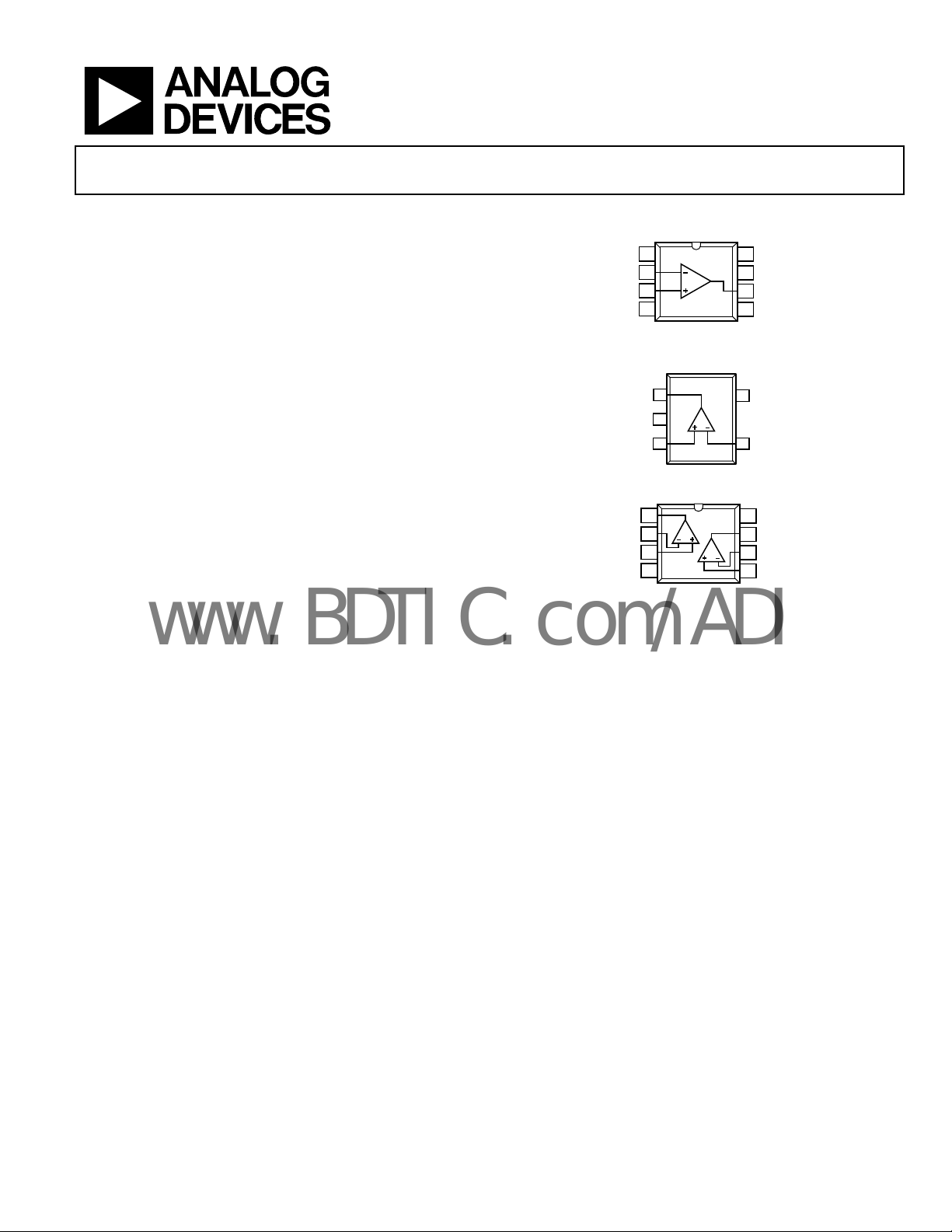
PIN CONFIGURATIONS
1
NC
–IN A
2
+IN A
3
AD8519
4
V–
NC = NO CONNECT
Figure 1. 8-Lead SOIC (R Suffix)
AD8519
1
OUT A
V–
2
+IN A
3
Figure 2. 5-Lead SC70 and SOT-23 (KS and RJ Suffixes)
1
OUT A
–IN A
+IN A
V–
Figure 3. 8-Lead SOIC and MSOP (R and RM Suffixes)
AD8529
2
3
4
NC
8
V+
7
6
OUT A
NC
5
1756-001
V+
5
4
–IN A
01756-002
V+
8
OUT B
7
6
–IN B
5
+IN B
01756-003
GENERAL DESCRIPTION
The AD8519 and AD8529 are rail-to-rail output bipolar
amplifiers with a unity gain bandwidth of 8 MHz and a typical
voltage offset of less than 1 mV. The AD8519 brings precision
and bandwidth to the SC70 and SOT-23 packages. The low
supply current makes the AD8519/AD8529 ideal for batterypowered applications. The rail-to-rail output swing of the
AD8519/AD8529 is larger than standard video op amps, making
them useful in applications that require greater dynamic range
than standard video op amps. The 2.9 V/μs slew rate makes the
AD8519/AD8529 a good match for driving ASIC inputs such as
voice codecs.
The small SC70 package makes it possible to place the AD8519
ne
xt to sensors, reducing external noise pickup.
The AD8519/AD8529 is specified over the extended industrial
(−40°C t
o +125°C) temperature range. The AD8519 is available
in 5-lead SC70 and 5-lead SOT-23 packages, and an 8-lead
SOIC surface-mount package. The AD8529 is available in 8-lead
SOIC and 8-lead MSOP packages.
Rev. D
Information furnished by Analog Devices is believed to be accurate and reliable. However, no
responsibility is assumed by Anal og Devices for its use, nor for any infringements of patents or ot her
rights of third parties that may result from its use. Specifications subject to change without notice. No
license is granted by implication or otherwise under any patent or patent rights of Analog Devices.
Trademarks and registered trademarks are the property of their respective owners.
One Technology Way, P.O. Box 9106, Norwood, MA 02062-9106, U.S.A.
Tel: 781.329.4700 www.analog.com
Fax: 781.461.3113 ©1998–2007 Analog Devices, Inc. All rights reserved.

AD8519/AD8529
www.BDTIC.com/ADI
TABLE OF CONTENTS
Features.............................................................................................. 1
ESD Caution...................................................................................7
Applications....................................................................................... 1
Pin Configurations ........................................................................... 1
General Description ......................................................................... 1
Revision History ............................................................................... 2
Specifications..................................................................................... 3
Electrical Characteristics ............................................................. 3
Absolute Maximum Ratings............................................................ 7
Thermal Resistance ...................................................................... 7
REVISION HISTORY
5/07—Rev. C to Rev. D
Changes to Features.......................................................................... 1
Changes to General Description .................................................... 1
Changes to Two-Element Bridge Amplifier Section.................. 13
Updated Outline Dimensions....................................................... 14
2/03—Rev. B to Rev. C
Changed μSOIC to MSOP.................................................Universal
Changed SO-8 to R-8.........................................................Universal
Changes to Precision Full-Wave Rectifier section ....................... 9
Changes to 10× Microphone Preamp Meets PC99
Specifications section................................................................... 9
Updated Outline Dimensions....................................................... 12
Typical Performance Characteristics..............................................8
Applications Information.............................................................. 12
Maximum Power Dissipation................................................... 12
Precision Full-Wave Rectifier ................................................... 12
10× Microphone Preamp Meets PC99 Specifications........... 13
Two-Element Varying Bridge Amplifier................................. 13
Outline Dimensions....................................................................... 14
Ordering Guide .......................................................................... 15
Rev. D | Page 2 of 16

AD8519/AD8529
www.BDTIC.com/ADI
SPECIFICATIONS
ELECTRICAL CHARACTERISTICS
VS = 5.0 V, V− = 0 V, VCM = 2.5 V, TA = 25°C, unless otherwise noted.
Table 1.
Parameter Symbol Conditions Min Typ Max Unit
INPUT CHARACTERISTICS
Offset Voltage VOS AD8519AKS, AD8519ART 600 1100 μV
−40°C ≤ TA ≤ +125°C 800 1300 μV
AD8519AR (R-8), AD8529 600 1000 μV
−40°C ≤ TA ≤ +125°C 1100 μV
Input Bias Current IB 300 nA
−40°C ≤ TA ≤ +125°C 400 nA
Input Offset Current IOS ±50 nA
−40°C ≤ TA ≤ +125°C ±100 nA
Input Voltage Range V
Common-Mode Rejection Ratio CMRR 0 V ≤ VCM ≤ 4.0 V, −40°C ≤ TA ≤ +125°C 63 100 dB
Large Signal Voltage Gain A
R
R
Offset Voltage Drift ∆VOS/∆T 2 μV/°C
Bias Current Drift ∆IB/∆T 500 pA/°C
OUTPUT CHARACTERISTICS
Output Voltage Swing High V
−40°C ≤ TA ≤ +125°C 4.90 V
I
Output Voltage Swing Low V
−40°C ≤ TA ≤ +125°C 80 mV
I
Short-Circuit Current I
Maximum Output Current I
POWER SUPPLY
Power Supply Rejection Ratio PSRR VS = 2.7 V to 7 V 110 dB
−40°C ≤ TA ≤ +125°C 80 dB
Supply Current/Amplifier I
−40°C ≤ TA ≤ +125°C 1400 μA
DYNAMIC PERFORMANCE
Slew Rate SR 1 V < V
Settling Time tS To 0.01% 1200 ns
Gain Bandwidth Product GBP 8 MHz
Phase Margin Φm 60 Degrees
NOISE PERFORMANCE
Voltage Noise en p-p 0.1 Hz to 10 Hz 0.5 μV p-p
Voltage Noise Density en f = 1 kHz 10 nV/√Hz
Current Noise Density in f = 1 kHz 0.4 pA/√Hz
0 4 V
CM
R
VO
I
OH
I
OL
Short to ground, instantaneous ±70 mA
SC
±25 mA
OUT
V
SY
= 2 kΩ, 0.5 V < V
L
= 10 kΩ, 0.5 V < V
L
= 10 kΩ, −40°C ≤ TA ≤ +125°C 30 V/mV
L
= 250 μA
L
= 5 mA 4.80 V
L
= 250 μA
L
= 5 mA 200 mV
L
= 2.5 V 600 1200 μA
OUT
< 4 V, RL = 10 kΩ 2.9 V/μs
OUT
< 4.5 V 30 V/mV
OUT
< 4.5 V 50 100 V/mV
OUT
Rev. D | Page 3 of 16

AD8519/AD8529
www.BDTIC.com/ADI
VS = 3.0 V, V− = 0 V, VCM = 1.5 V, TA = 25°C, unless otherwise noted.
Table 2.
Parameter Symbol Conditions Min Typ Max Unit
INPUT CHARACTERISTICS
Offset Voltage VOS AD8519AKS, AD8519ART 700 1200 μV
−40°C ≤ TA ≤ +125°C 900 1400 μV
AD8519AR (R-8), AD8529 700 1100 μV
−40°C ≤ TA ≤ +125°C 1200 μV
Input Bias Current IB 300 nA
Input Offset Current IOS ±50 nA
Input Voltage Range VCM 0 2 V
Common-Mode Rejection Ratio CMRR 0 V ≤ VCM ≤ 2.0 V,
−40°C ≤ TA ≤ +125°C 55 75 dB
Large Signal Voltage Gain AVO RL = 2 kΩ, 0.5 V < V
R
OUTPUT CHARACTERISTICS
Output Voltage Swing High VOH IL = 250 μA 2.90 V
I
Output Voltage Swing Low VOL IL = 250 μA 100 mV
I
POWER SUPPLY
Power Supply Rejection Ratio PSRR VS = 2.5 V to 7 V, −40°C ≤ TA ≤ +125°C 60 80 dB
Supply Current/Amplifier ISY V
−40°C ≤ TA ≤ +125°C 1300 μA
DYNAMIC PERFORMANCE
Slew Rate SR RL = 10 kΩ 1.5 V/μs
Settling Time tS To 0.01% 2000 ns
Gain Bandwidth Product GBP 6 MHz
Phase Margin Φm 55 Degrees
NOISE PERFORMANCE
Voltage Noise Density en f = 1 kHz 10 nV/√Hz
Current Noise Density in f = 1 kHz 0.4 pA/√Hz
= 10 kΩ 20 30 V/mV
L
= 5 mA 2.80 V
L
= 5 mA 200 mV
L
= 1.5 V 600 1100 μA
OUT
< 2.5 V 20 V/mV
OUT
Rev. D | Page 4 of 16

AD8519/AD8529
www.BDTIC.com/ADI
VS = 2.7 V, V− = 0 V, VCM = 1.35 V, TA = 25°C, unless otherwise noted.
Table 3.
Parameter Symbol Conditions Min Typ Max Unit
INPUT CHARACTERISTICS
Offset Voltage VOS AD8519AKS, AD8519ART 700 1400 μV
−40°C ≤ TA ≤ +125°C 900 1600 μV
AD8519AR (R-8), AD8529 700 1200 μV
−40°C ≤ TA ≤ +125°C 1300 μV
Input Bias Current IB 300 nA
Input Offset Current I
Input Voltage Range VCM 0 2 V
Common-Mode Rejection Ratio CMRR 0 V ≤ VCM ≤ 1.7 V, −40°C ≤ TA ≤ +125°C 55 75 dB
Large Signal Voltage Gain AVO RL = 2 kΩ, 0.5 V < V
R
OUTPUT CHARACTERISTICS
Output Voltage Swing High V
I
Output Voltage Swing Low V
I
POWER SUPPLY
Power Supply Rejection Ratio PSRR VS = 2.5 V to 7 V
−40°C ≤ TA ≤ +125°C 60 80 dB
Supply Current/Amplifier ISY V
−40°C ≤ TA ≤ +125°C 1300 μA
DYNAMIC PERFORMANCE
Slew Rate SR RL = 10 kΩ 1.5 V/μs
Settling Time tS To 0.01% 2000 ns
Gain Bandwidth Product GBP 6 MHz
Phase Margin Φm 55 Degrees
NOISE PERFORMANCE
Voltage Noise Density en f = 1 kHz 10 nV/√Hz
Current Noise Density in f = 1 kHz 0.4 pA/√Hz
±50 nA
OS
< 2.2 V 20 V/mV
OUT
= 10 kΩ 20 30 V/mV
L
I
OH
I
OL
= 250 μA 2.60 V
L
= 5 mA 2.50 V
L
= 250 μA 100 mV
L
= 5 mA 200 mV
L
= 1.35 V 600 1100 μA
OUT
Rev. D | Page 5 of 16

AD8519/AD8529
www.BDTIC.com/ADI
VS = 5.0 V, V− = −5 V, VCM = 0 V, TA = 25°C, unless otherwise noted.
Table 4.
Parameter Symbol Conditions Min Typ Max Unit
INPUT CHARACTERISTICS
Offset Voltage VOS AD8519AKS, AD8519ART 600 1100 μV
−40°C ≤ TA ≤ +125°C 800 1300 μV
AD8519AR (R-8), AD8529 600 1000 μV
−40°C ≤ TA ≤ +125°C 1100 μV
Input Bias Current IB VCM = 0 V 300 nA
V
Input Offset Current IOS VCM = 0 V ±50 nA
V
Input Voltage Range VCM −5 +4 V
Common-Mode Rejection Ratio CMRR −4.9 V ≤ VCM ≤ +4.0 V,
−40°C ≤ TA ≤ +125°C 70 100 dB
Large Signal Voltage Gain AVO RL = 2 kΩ 30 V/mV
R
−40°C ≤ TA ≤ +125°C 25 V/mV
Offset Voltage Drift ∆VOS/∆T 2 μV/°C
Bias Current Drift ∆IB/∆T 500 pA/°C
OUTPUT CHARACTERISTICS
Output Voltage Swing High V
−40°C ≤ TA ≤ +125°C 4.90 V
I
Output Voltage Swing Low VOL IL = 250 μA
−40°C ≤ TA ≤ +125°C −4.90 V
I
Short-Circuit Current I
Maximum Output Current I
POWER SUPPLY
Power Supply Rejection Ratio PSRR VS = ±1.5 V to ±6 V, −40°C ≤ TA ≤ +125°C 60 100 dB
Supply Current/Amplifier I
−40°C ≤ TA ≤ +125°C 1400 μA
DYNAMIC PERFORMANCE
Slew Rate SR −4 V < V
Settling Time tS To 0.01% 1000 ns
Gain Bandwidth Product GBP 8 MHz
Phase Margin Φm 60 Degrees
NOISE PERFORMANCE
Voltage Noise Density en f = 1 kHz 10
Current Noise Density in f = 1 kHz 0.4
I
OH
Short to ground, instantaneous ±70 mA
SC
±25 mA
OUT
V
SY
= 0 V, −40°C ≤ TA ≤ +125°C 400 nA
CM
= 0 V, −40°C ≤ TA ≤ +125°C ±100 nA
CM
= 10 kΩ 50 200 V/mV
L
= 250 μA
L
= 5 mA 4.80 V
L
= 5 mA −4.80 V
L
= 0 V 600 1200 μA
OUT
< +4 V, RL = 10 kΩ 2.9 V/μs
OUT
nV/√Hz
pA/√Hz
Rev. D | Page 6 of 16

AD8519/AD8529
www.BDTIC.com/ADI
ABSOLUTE MAXIMUM RATINGS
Table 5.
Parameter Rating
Supply Voltage ±6 V
Input Voltage1 ±6 V
Differential Input Voltage2 ±0.6 V
Storage Temperature Range −65°C to +150°C
Operating Temperature Range −40°C to +125°C
Junction Temperature Range −65°C to +150°C
Lead Temperature Range
(Soldering, 60 sec)
1
For supply voltages less than ±6 V, the input voltage is limited to less than or
equal to the supply voltage.
2
For differential input voltages greater than ±0.6 V, the input current should
be limited to less than 5 mA to prevent degradation or destruction of the
input devices.
Stresses above those listed under Absolute Maximum Ratings
may cause permanent damage to the device. This is a stress
rating only; functional operation of the device at these or any
other conditions above those indicated in the operational
section of this specification is not implied. Exposure to absolute
maximum rating conditions for extended periods may affect
device reliability.
300°C
THERMAL RESISTANCE
Table 6.
Package Type θ
5-Lead SC70 (KS) 376 126 °C/W
5-Lead SOT-23 (RJ) 230 146 °C/W
8-Lead SOIC (R) 158 43 °C/W
8-Lead MSOP (RM) 210 45 °C/W
1
θJA is specified for worst-case conditions, that is, θJA is specified for device
soldered in circuit board for SOT-23 and SOIC packages.
1
θJC Unit
JA
ESD CAUTION
Rev. D | Page 7 of 16

AD8519/AD8529
www.BDTIC.com/ADI
TYPICAL PERFORMANCE CHARACTERISTICS
60
= 5V
V
S
T
= 25°C
A
50
COUNT = 395 OP AMP S
40
VS = 5V
T
= 25°C
A
0
40
30
20
QUANTITY O F AMPLIFIERS
10
0
–1.0 –0.6 –0.2 0.2 0.6 1.0
INPUT OFFSET VOLTAGE (mV)
Figure 4. Input Offset Voltage Distribution
600
550
500
SUPPLY CURRENT (µA)
–40
–80
–120
–160
INPUT BIAS CURRENT (nA)
–200
01756-004
–240
012345
COMMON-MODE VOLTAGE (V)
1756-007
Figure 7. Input Bias Current vs. Common-Mode Voltage
120
100
80
60
40
COMMON-MO DE REJECTIO N (dB)
= 5V
V
S
450
0246810
SUPPLY VOLTAGE (V)
Figure 5. Supply Current per Amplifier vs. Supply Voltage
800
700
600
500
SUPPLY CURRENT (µA)
400
300
–50 –25 0 25 50 75 100 125 150
VS = 10V
TEMPERATURE ( °C)
VS = 5V
VS = 2.7V, 3. 0V
Figure 6. Supply Current per Amplifier vs. Temperature
01756-005
12
01756-006
20
01234
COMMON-MODE VOLTAGE (V)
Figure 8. Common-Mode Rejection vs. Common-Mode Voltage
50
40
30
20
10
0
OPEN-LOOP GAIN (dB)
–10
–20
–30
100k 1M 10M 100M
GAIN
FREQUENCY (Hz)
PHASE
VS = 5V
= 25°C
T
A
Figure 9. Open-Loop Gain, Phase vs. Frequency
01756-008
5
45
90
135
180
PHASE SHIFT (Degrees)
225
270
1756-009
Rev. D | Page 8 of 16

AD8519/AD8529
www.BDTIC.com/ADI
60
40
20
0
CLOSED-LOOP GAIN (dB)
–20
–40
10k 100k 1M 10M 100M
FREQUENCY (Hz)
VS = 5V
R
T
C
Figure 10. Closed-Loop Gain vs. Frequency
110
100
90
80
70
60
CMRR (dB)
50
40
30
20
1k 10k 100k 1M 10M
FREQUENCY (Hz)
VS = 5V
T
Figure 11. CMRR vs. Frequency
= 830Ω
L
= 25°C
A
≤ 5pF
L
= 25°C
A
01756-010
01756-011
60
VS = 5V
V
= 2.5V
CM
R
= 10kΩ
L
50
T
= 25°C
A
V
= ±50mV
IN
40
30
OVERSHOOT (%)
20
10
0
10 100 1k
4
VS = 5V
T
3
2
1
0
–1
STEP SIZE (V)
–2
–3
–4
01
+OS
CAPACITANCE (pF )
Figure 13. Overshoot v
= 25°C
A
SETTLING TIME (µs)
s. Capacitance Load
1%
1%
–OS
0.1%
0.1%
Figure 14. Step Size vs. Settling Time
01756-013
01756-014
2
90
80
70
60
50
40
PSRR (dB)
30
20
10
0
+PSRR
1k 10k 100k 1M 10M
–PSRR
FREQUENCY (Hz)
Figure 12. PSRR vs. Frequency
VS = 5V
T
= 25°C
A
01756-012
Rev. D | Page 9 of 16
5
4
DISTORT ION < 1%
3
2
1
MAXIMUM OUTPUT SWING (V p-p)
0
10k 100k 1M 10M
FREQUENCY (Hz)
VS = 5V
AVCC = 1
R
T
C
Figure 15. Output Swing vs. Frequency
= 10kΩ
L
= 25°C
A
= 15pF
L
01756-015

AD8519/AD8529
www.BDTIC.com/ADI
300
VS = 5V
T
= 25°C
A
250
200
AVCC = 10
150
100
OUTPUT IMPEDANCE (Ω)
50
AVCC = 1
VS = ±2.5V
A
= 100kΩ
V
e
= 0.4µV p-p
n
0
100k 1M 10M
FREQUENCY (Hz)
Figure 16. Output Imped
80
VS = 5V
T
= 25°C
A
70
60
50
40
30
20
VOLTAGE NOISE DENSITY (nV/ Hz)
10
0
10 100 1k 10k
ance vs. Frequency
FREQUENCY (Hz)
Figure 17. Voltage Noise Density
8
VS = 5V
= 25°C
T
7
A
6
5
4
01756-016
1s20mV
01756-019
Figure 19. 0.1 Hz to 10 Hz Noise
VS = ±2.5V
= 6V p-p
V
IN
= 1
A
V
01756-017
20µs1V
01756-020
Figure 20. No Phase Reversal
VS = ±2.5V
AVCC = 1
= 25°C
T
A
= 100pF
C
L
= 10kΩ
R
L
3
2
CURRENT NOISE DENSIT Y (pA/ Hz)
1
0
10 100 1k 10k
FREQUENCY (Hz)
Figure 18. Current Noise Density
01756-018
Figure 21. Small Signal Transient Response
Rev. D | Page 10 of 16
500ns20mV
01756-021

AD8519/AD8529
www.BDTIC.com/ADI
VS = ±2.5V
AVCC = 1
= 25°C
T
A
= 100pF
C
L
50µs500mV
Figure 22. Large Signal Transient Response
01756-022
Rev. D | Page 11 of 16

AD8519/AD8529
www.BDTIC.com/ADI
APPLICATIONS INFORMATION
MAXIMUM POWER DISSIPATION
The maximum power that can be safely dissipated by the
AD8519/AD8529 is limited by the associated rise in junction
temperature. The maximum safe junction temperature is 150°C
for these plastic packages. If this maximum is momentarily
exceeded, proper circuit operation is restored as soon as the
die temperature is reduced. Operating the product in an
overheated condition for an extended period can result in
permanent damage to the device.
PRECISION FULL-WAVE RECTIFIER
Slew rate is probably the most underestimated parameter when
designing a precision rectifier. Yet without a good slew rate,
large glitches are generated during the period when both diodes
are off.
The operation of the basic circuit (shown in Figure 23) should
b
e examined before considering the slew rate further. U1 is set
up to have two states of operation. D1 and D2 diodes switch the
output between the two states. State one is an inverter with a
gain of +1, and state two is a simple unity gain buffer where the
output is equal to the value of the virtual ground. The virtual
ground is the potential present at the noninverting node of the
U1. State one is active when V
ground. D2 is on in this condition. If V
ground, D2 turns off and D1 turns on. This causes the output of
U1 to simply buffer the virtual ground and this configuration is
state two. Therefore, the function of U1, which results from
these two states of operation, is a half-wave inverter. The U2
function takes the inverted half wave at a gain of two and sums
it into the original V
OUT
wave, which outputs a rectified full wave.
IN
VVV
ININ
This type of rectifier can be very precise if the following
el
ectrical parameters are adhered to:
• All passive components should be of tight tolerance, 1% for
resistors and 5% for capacitors.
• If the application circuit requires high impedance (that is,
direct sensor interface), then an FET amplifier is a better
choice than the AD8519.
• An amp such as the AD8519, which has a great slew rate
specification, yields the best result because the circuit
involves switching.
is larger than the virtual
IN
IN
1
−
02
<−=
drops below virtual
R1
V
IN
10kΩ
R6
5kΩ
Switching glitches are caused when D1 and D2 are both
momentarily off. This condition occurs every time the input
signal is equal to the virtual ground potential. When this
condition occurs, the U1 stage is taken out of the V
and V
is equal to VIN × R5 × (R4 || R1 + R2 + R3). Note that
OUT
Node A should be V
condition, Node A is simply tracking V
input centered around virtual ground, glitches are generated
at the sharp negative peaks of the rectified sine wave. If the
glitches are hard to notice on an oscilloscope, raise the frequency of the sine wave until they become apparent. The size
of the glitches is proportional to the input frequency, the diode
turn-on potential (0.2 V or 0.65 V), and the slew rate of the op amp.
R6 and R7 are both necessary to limit the amount of bias
c
urrent related voltage offset. Unfortunately, there is no perfect
value for R6 because the impedance at the inverting node is
altered as D1 and D2 switch. Therefore, there is also some
unresolved bias current related offset. To minimize this offset,
use lower value resistors or choose an FET amplifier if the
optimized offset is still intolerable.
The AD8519 offers a unique combination of speed vs. power
tio at 2.7 V single supply, small size (SC70 and SOT-23), and low
ra
noise that makes it an ideal choice for most high volume and
high precision rectifier circuits.
R4
10kΩ
R2
NODE A
10kΩ
D1
1N914
U1
VIRTUAL GROUND =
Figure 23. Precision Full-Wave Rectifier
IN
1N914
AD8519
inverted or virtual ground, but in this
R3
4.99kΩ
D2
R7
3.32kΩ
V
CC
2
. Given a sine wave
IN
R5
10kΩ
U2
AD8519
equation
OUT
V
OUT
01756-023
Rev. D | Page 12 of 16

AD8519/AD8529
F
V
www.BDTIC.com/ADI
10× MICROPHONE PREAMP MEETS PC99 SPECIFICATIONS
This circuit, while lacking a unique topology, is anything but
featureless when an AD8519 is used as the op amp. This preamp
gives 20 dB gain over a frequency range of 20 Hz to 20 kHz and
is fully PC99 compliant in all parameters including THD + N,
dynamic range, frequency range, amplitude range, and crosstalk.
Not only does this preamp comply with the PC99 specifications,
it far surpasses them. In fact, when the input noise is 120 dB,
this preamp has a V
able for most professional 20-bit audio systems. At 120 dB THD
+ N in unity gain, the AD8519 is suitable for 24-bit professional
audio systems. In other words, the AD8519 will not be the
limiting performance factor in audio systems despite its small
size and low cost.
Slew rate related distortion is not present at the lower voltages
bec
ause the AD8519 is so fast at 2.1 V/μs. A general rule of
thumb for determining the necessary slew rate for an audio
system is to take the maximum output voltage range of the
device, given the design’s power rails, and divide by two. In
Figure 24, the power rails are 2.7 V and the output is rail-to-rail.
En
ter these numbers into the equation: 2.7/2 = 1.35 V, and the
minimum ideal slew rate is 1.35 V/μs.
While this data sheet gives only one audio example, many audio
cuits are enhanced with the use of the AD8519. Examples
cir
include: active audio filters such as bass, treble, and equalizers;
PWM filters at the output of audio DACs; buffers and summers
for mixing stations; and gain stages for volume control.
2.7V
MIC
1kΩ
IN
1nF
NPO
C1
1µF
noise of around 100 dB, which is suit-
OUT
240p
30.9kΩ
2.7V
3.09kΩ
AD8519
CODEC LI NE IN
OR MIC IN
48kΩ
TWO-ELEMENT VARYING BRIDGE AMPLIFIER
There are a host of bridge configurations available to designers.
For a complete analysis, look at the ubiquitous bridge and its
different forms. Refer to the 1992
Figure 25 is a schematic of a two-element varying bridge. This
co
nfiguration is commonly found in pressure and flow transducers. With a two-element varying bridge, the signal is 2× as
compared to a single-element varying bridge. The advantages
of this type of bridge are gain setting range and single-supply
application. Negative characteristics are nonlinear operation
and required R matching. Given these sets of conditions,
requirements, and characteristics, the AD8519 can be successfully
used in this configuration because of its rail-to-rail output and
low offset. Perhaps the greatest benefits of the AD8519, when
used in the bridge configuration, are the advantages it can bring
when placed in a remote bridge sensor. For example, the tiny
SC70 and SOT-23 packages reduce the overall sensor size; low
power allows for remote powering via batteries or solar cells,
high output current drive to drive a long cable; and 2.7 V
operation for two-cell operation.
2.7
R
R R
Figure 25. Two-Element Varying Bridge Amplifier
1
Adolfo Garcia and James Wong, Chapter 2, 1992, Amplifier Applications Guide.
Amplifier Applications Guide
R
F
R
AD8519
R
F
1756-025
1
.
46.4kΩ 93.1kΩ
10µF ELECT
Figure 24. 10× Microphone Preamplifier
2.7V
01756-024
Rev. D | Page 13 of 16

AD8519/AD8529
www.BDTIC.com/ADI
OUTLINE DIMENSIONS
5.00 (0.1968)
4.80 (0.1890)
4.00 (0.1574)
3.80 (0.1497)
0.25 (0.0098)
0.10 (0.0040)
COPLANARITY
0.10
CONTROLL ING DIMENSI ONS ARE IN MILLIME TERS; INCH DIM ENSIONS
(IN PARENTHESES) ARE ROUNDED-OF F MILLIMETER E QUIVALENTS FOR
REFERENCE ONLY AND ARE NOT APPROPRI ATE FOR USE IN DESI GN.
85
1
1.27 (0.0500)
SEATING
PLANE
COMPLIANT TO JEDEC STANDARDS MS-012-A A
BSC
6.20 (0.2441)
5.80 (0.2284)
4
1.75 (0.0688)
1.35 (0.0532)
0.51 (0.0201)
0.31 (0.0122)
8°
0°
0.25 (0.0098)
0.17 (0.0067)
0.50 (0.0196)
0.25 (0.0099)
Figure 26. 8-Lead Standard Small Outline Package [SOIC_N]
row Body
Nar
(R-8)
Dimensions shown in millimeters and (inches)
2.20
2.00
1.80
1.35
1.25
1.15
PIN 1
1.00
0.90
0.70
0
.
1
0
A
M
X
0.10 COPLANARITY
123
0.30
0.15
COMPLIANT TO JEDEC STANDARDS MO-203-AA
45
0.65 BSC
2.40
2.10
1.80
1.10
0.80
SEATING
PLANE
0.40
0.10
0.22
0.08
Figure 28. 5-Lead Thin Shrink Small Outline Transistor Package [SC70]
(K
S-5)
Dimensions shown in millimeters
1.27 (0.0500)
0.40 (0.0157)
0.46
0.36
0.26
45°
0.95
0.85
0.75
0.15
0.00
COPLANARITY
012407-A
1.60 BSC
PIN 1
1.30
1.15
0.90
0.15 MAX
Figure 29. 5-Lead Small Outline Transistor Package [SOT-23]
3.20
3.00
2.80
8
5
4
SEATING
PLANE
5.15
4.90
4.65
1.10 MAX
0.23
0.08
8°
0°
3.20
3.00
1
2.80
PIN 1
0.65 BSC
0.38
0.22
0.10
COMPLIANT TO JEDEC STANDARDS MO-187-AA
Figure 27. 8-Lead Mini Small Outline Package [MSOP]
(RM-8)
Dimensions shown in millimeters
2.90 BSC
5
123
COMPLIANT TO JEDEC STANDARDS MO-178-A A
1.90
BSC
0.50
0.30
4
2.80 BSC
0.95 BSC
1.45 MAX
SEATING
PLANE
0.22
0.08
10°
5°
0°
(RJ-5)
Dimensions shown in millimeters
0.80
0.60
0.40
0.60
0.45
0.30
Rev. D | Page 14 of 16

AD8519/AD8529
www.BDTIC.com/ADI
ORDERING GUIDE
Temperature
Model
AD8519AKS-REEL7 −40°C to +125°C 5-Lead SC70 KS-5 A3B
AD8519AKSZ-REEL71 −40°C to +125°C 5-Lead SC70 KS-5 A11
AD8519ART-REEL −40°C to +125°C 5-Lead SOT-23 RJ-5 A3A
AD8519ART-REEL7 −40°C to +125°C 5-Lead SOT-23 RJ-5 A3A
AD8519ARTZ-REEL1 −40°C to +125°C 5-Lead SOT-23 RJ-5 A3A#
AD8519ARTZ-REEL71 −40°C to +125°C 5-Lead SOT-23 RJ-5 A3A#
AD8519AR −40°C to +125°C 8-Lead SOIC_N R-8
AD8519AR-REEL −40°C to +125°C 8-Lead SOIC_N R-8
AD8519AR-REEL7 −40°C to +125°C 8-Lead SOIC_N R-8
AD8519ARZ1 −40°C to +125°C 8-Lead SOIC_N R-8
AD8519ARZ-REEL −40°C to +125°C 8-Lead SOIC_N R-8
AD8519ARZ-REEL71 −40°C to +125°C 8-Lead SOIC_N R-8
AD8529AR −40°C to +125°C 8-Lead SOIC_N R-8
AD8529AR-REEL −40°C to +125°C 8-Lead SOIC_N R-8
AD8529ARZ1 −40°C to +125°C 8-Lead SOIC_N R-8
AD8529ARZ-REEL1 −40°C to +125°C 8-Lead SOIC_N R-8
AD8529ARM-REEL −40°C to +125°C 8-Lead MSOP RM-8 A5A
AD8529ARMZ-REEL
1
Z = RoHS compliant part, # denotes RoHS compliant part may be top or bottom marked.
1
R
ange Package Description Package Option Branding Information
−40°C to +125°C 8-Lead MSOP RM-8 A5A#
Rev. D | Page 15 of 16

AD8519/AD8529
www.BDTIC.com/ADI
NOTES
©1998–2007 Analog Devices, Inc. All rights reserved. Trademarks and
registered trademarks are the property of their respective owners.
C01756–0–5/07(D)
Rev. D | Page 16 of 16
 Loading...