

Page 1

20 μA Maximum, Rail-to-Rail I/O,
www.BDTIC.com/ADI
Zero Input Crossover Distortion Amplifiers
FEATURES
PSRR: 100 dB minimum
CMRR: 105 dB typical
Very low supply current: 20 μA per amp maximum
1.8 V to 5.5 V single-supply operation
Rail-to-rail input and output
Low noise
2.8 μV p-p from 0.1 Hz to 10 Hz
45 nV/√Hz @ 1 kHz
2.5 mV offset voltage maximum
Very low input bias current: 1 pA typical
APPLICATIONS
Pressure and position sensors
Remote security
Bio sensors
IR thermometers
Battery-powered consumer equipment
Hazard detectors
GENERAL DESCRIPTION
The AD8506 is a dual micropower amplifier featuring rail-torail input and output swings while operating from a 1.8 V to 5.5 V
single power supply.
Using a novel circuit technology, these low cost amplifiers offer
ero crossover distortion (excellent PSRR and CMRR perform-
z
ance) and very low bias current, while operating with a supply
current of less than 20 μA per amplifier. This amplifier offers
the lowest noise in its power class.
This combination of features makes the AD8506 amplifier an
deal choice for battery-powered applications because it mini-
i
mizes errors due to power supply voltage variations over the
AD8506
PIN CONFIGURATION
1
OUT A
–IN A
+IN A
Figure 1. 8-Lead MSOP (RM Suffix)
V–
AD8506
2
TOP VIEW
3
(Not to Scale)
4
lifetime of the battery and maintains high CMRR even for a
il-to-rail input op amp.
ra
Remote battery-powered sensors, handheld instrumentation
a
nd consumer equipment, hazard detection (for example, smoke,
fire, and gas), and patient monitors can benefit from the features
of the AD8506 amplifier.
The AD8506 is specified for both the industrial temperature
r
ange of −40°C to +85°C and the extended industrial temperature
range of −40°C to +125°C. AD8506 dual amplifiers are available
in 8-lead MSOP packages.
8
7
6
5
V+
OUT B
–IN B
+IN B
06900-002
Rev. 0
Information furnished by Analog Devices is believed to be accurate and reliable. However, no
responsibility is assumed by Anal og Devices for its use, nor for any infringements of patents or ot her
rights of third parties that may result from its use. Specifications subject to change without notice. No
license is granted by implication or otherwise under any patent or patent rights of Analog Devices.
Trademarks and registered trademarks are the property of their respective owners.
One Technology Way, P.O. Box 9106, Norwood, MA 02062-9106, U.S.A.
Tel: 781.329.4700 www.analog.com
Fax: 781.461.3113 ©2007 Analog Devices, Inc. All rights reserved.
Page 2

AD8506
www.BDTIC.com/ADI
TABLE OF CONTENTS
Features.............................................................................................. 1
Applications....................................................................................... 1
Pin Configuration............................................................................. 1
General Description ......................................................................... 1
Revision History ............................................................................... 2
Specifications..................................................................................... 3
Electrical Characteristics ............................................................. 3
REVISION HISTORY
11/07—Revision 0: Initial Version
Absolute Maximum Ratings ............................................................5
Thermal Resistance.......................................................................5
ESD Caution...................................................................................5
Typical Performance Characteristics ..............................................6
Outline Dimensions....................................................................... 12
Ordering Guide .......................................................................... 12
Rev. 0 | Page 2 of 12
Page 3

AD8506
www.BDTIC.com/ADI
SPECIFICATIONS
ELECTRICAL CHARACTERISTICS
VSY = 5 V, VCM = VSY/2, TA = 25°C, RL = 100 kΩ to GND, unless otherwise noted.
Table 1.
Parameter Symbol Conditions Min Typ Max Unit
INPUT CHARACTERISTICS
Offset Voltage VOS 0 V < VCM < 5 V 0.5 2.5 mV
−40°C < TA < +125°C 3 mV
Input Bias Current IB 1 10 pA
−40°C < TA < +85°C 100 pA
−40°C < TA < +125°C 600 pA
Input Offset Current IOS 0.5 5 pA
−40°C < TA < +85°C 50 pA
−40°C < TA < +125°C 130 pA
Input Voltage Range −40°C < TA < +125°C 0 5 V
Common-Mode Rejection Ratio CMRR VCM = 0 V to 5 V 90 105 dB
−40°C < TA < +85°C 90 dB
−40°C < TA < +125°C 85 dB
Large Signal Voltage Gain AVO 0.05 V < V
−40°C < TA < +125°C 100 dB
Offset Voltage Drift
Input Capacitance
OUTPUT CHARACTERISTICS
Output Voltage High VOH R
−40°C < TA < +125°C 4.98 V
R
−40°C < TA < +125°C 4.9 V
Output Voltage Low VOL R
−40°C < TA < +125°C 5 mV
R
−40°C < TA < +125°C 25 mV
Short-Circuit Limit ISC ±55 mA
POWER SUPPLY
Power Supply Rejection Ratio PSRR VS = 1.8 V to 5 V 100 110 dB
−40°C < TA < +85°C 100 dB
−40°C < TA < +125°C 95 dB
Supply Current/Amplifier ISY V
−40°C < TA < +125°C 25 μA
DYNAMIC PERFORMANCE
Slew Rate SR RL = 100 kΩ, CL = 10 pF,
Gain Bandwidth Product GBP 100 kHz
−3 dB Bandwidth 150 kHz
Phase Margin ΦM 60 Degrees
NOISE PERFORMANCE
Peak-to-Peak Noise e
Voltage Noise Density en f = 1 kHz 45 nV/√Hz
Current Noise Density in f = 1 kHz 80 fA/√Hz
/ΔT
ΔV
OS
C
DIFF
CCM
f = 0.1 Hz to 10 Hz 2.8 μV p-p
n p-p
−40°C < T
3 pF
4.2 pF
= 100 kΩ to GND 4.98 4.99 V
L
= 10 kΩ to GND 4.9 4.95 V
L
= 100 kΩ to VS 2 5 mV
L
= 10 kΩ to VS 10 25 mV
L
= VS/2 15 20 μA
O
= +1
A
V
< 4.95 V 105 120 dB
OUT
< +125°C 2 μV/°C
A
13 mV/μs
Rev. 0 | Page 3 of 12
Page 4

AD8506
www.BDTIC.com/ADI
VSY = 1.8 V, VCM = VSY/2, TA = 25°C, RL = 100 kΩ to GND, unless otherwise noted.
Table 2.
Parameter Symbol Conditions Min Typ Max Unit
INPUT CHARACTERISTICS
Offset Voltage VOS 0 V < VCM < 1.8 V 0.5 2.5 mV
−40°C < TA < +125°C 3 mV
Input Bias Current IB 1 10 pA
−40°C < TA < +85°C 100 pA
−40°C < TA < +125°C 600 pA
Input Offset Current IOS 0.5 5 pA
−40°C < TA < +85°C 50 pA
−40°C < TA < +125°C 100 pA
Input Voltage Range −40°C < TA < +125°C 0 1.8 V
Common-Mode Rejection Ratio CMRR VCM = 0 V to 1.8 V 85 100 dB
−40°C < TA < +85°C 85 dB
−40°C < TA < +125°C 80 dB
Large Signal Voltage Gain AVO 0.05V < V
< 1.75V 95 115 dB
OUT
−40°C < TA < +125°C 95 dB
Offset Voltage Drift
Input Capacitance
ΔV
C
DIFF
CCM
OS
/ΔT
−40°C < T
< +125°C 2.5 μV/°C
A
3 pF
4.2 pF
OUTPUT CHARACTERISTICS
Output Voltage High VOH R
= 100 kΩ to GND 1.78 1.79 V
L
−40°C < TA < +125°C 1.78 V
R
= 10 kΩ to GND 1.65 1.75 V
L
−40°C < TA < +125°C 1.65 V
Output Voltage Low VOL R
= 100 kΩ to VS 2 5 mV
L
−40°C < TA < +125°C 5 mV
R
= 10 kΩ to VS 12 25 mV
L
−40°C < TA < +125°C 25 mV
Short-Circuit Limit ISC ±6.5 mA
POWER SUPPLY
Power Supply Rejection Ratio PSRR VS = 1.8 V to 5 V 100 110 dB
−40°C < TA < +85°C 100 dB
−40°C < TA < +125°C 95 dB
Supply Current/Amplifier ISY V
= VS/2 16.5 20 μA
O
−40°C < TA < +125°C 25 μA
DYNAMIC PERFORMANCE
Slew Rate SR
= 100 kΩ, C
R
L
A
= +1
V
= 10 pF,
L
13 mV/μs
Gain Bandwidth Product GBP 100 kHz
−3 dB Bandwidth 150 kHz
Phase Margin Φ
M
60 Degrees
NOISE PERFORMANCE
Peak-to-Peak Noise e
f = 0.1 Hz to 10 Hz 2.8 μV p-p
n p-p
Voltage Noise Density en f = 1 kHz 45 nV/√Hz
Current Noise Density in f = 1 KHz 80 fA/√Hz
Rev. 0 | Page 4 of 12
Page 5
AD8506
www.BDTIC.com/ADI
ABSOLUTE MAXIMUM RATINGS
Table 3.
Parameter Rating
Supply Voltage 5.5 V
Input Voltage ±VSY
Differential Input Voltage1 ±VSY
Output Short-Circuit Duration to GND Indefinite
Storage Temperature Range −65°C to +150°C
Operating Temperature Range −40°C to +125°C
Junction Temperature Range −65°C to +150°C
Lead Temperature (Soldering, 60 sec) 300°C
1
Differential input voltage is limited to 5.5 V or the supply voltage, whichever
is less.
Stresses above those listed under Absolute Maximum Ratings
y cause permanent damage to the device. This is a stress
ma
rating only; functional operation of the device at these or any
other conditions above those indicated in the operational
section of this specification is not implied. Exposure to absolute
maximum rating conditions for extended periods may affect
device reliability.
THERMAL RESISTANCE
θJA is specified for the worst-case conditions, that is, a device
soldered in a circuit board for surface-mount packages.
Table 4. Thermal Resistance
Package Type θJA θ
8-Lead MSOP (RM) 190 44 °C/W
Unit
JC
ESD CAUTION
Rev. 0 | Page 5 of 12
Page 6
AD8506
www.BDTIC.com/ADI
TYPICAL PERFORMANCE CHARACTERISTICS
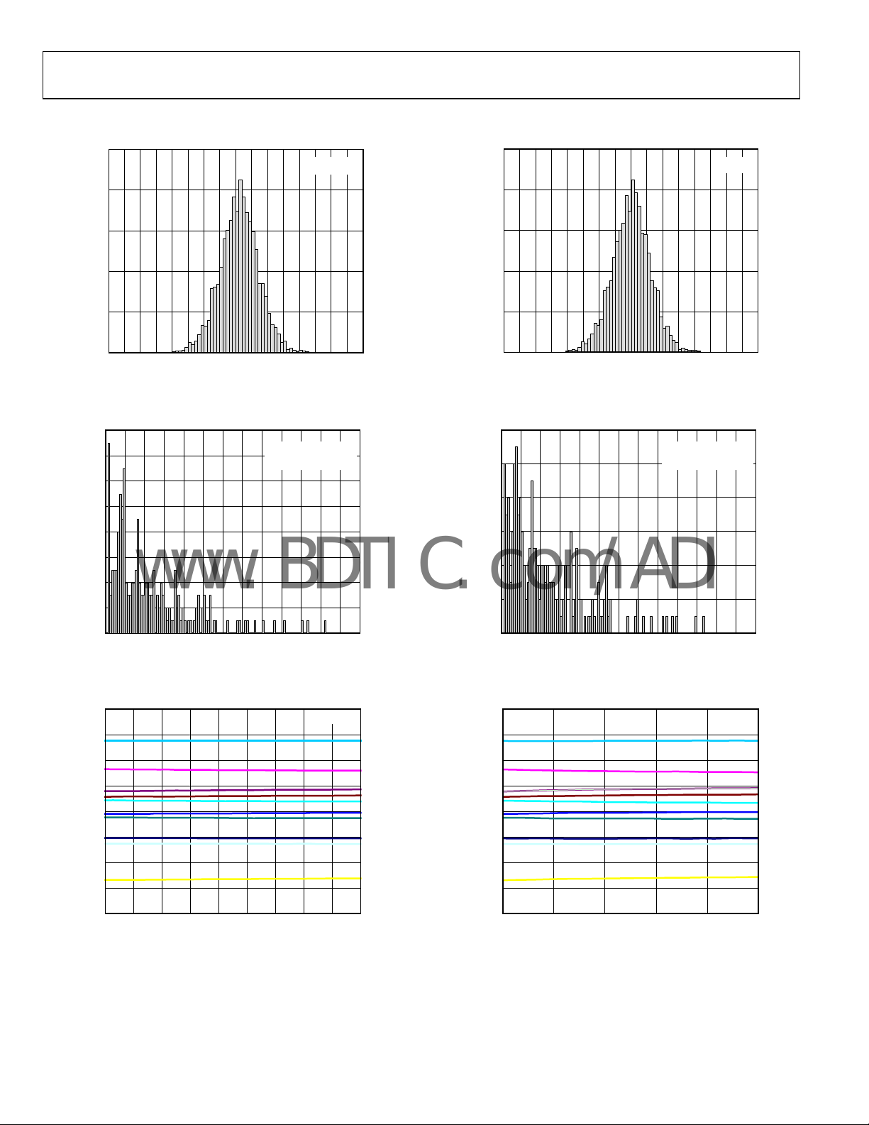
250
VSY = 1.8V
250
VSY = 5V
200
150
100
NUMBER OF AMPLIFIERS
50
0
–4 –1–3 0–2 1 2 3 4
VOS (mV)
Figure 2. Input Offset Voltage Distribution
16
VSY = 1.8V
–40°C < T
NUMBER OF AMPLIFIERS
14
12
10
8
6
4
2
< +125°C
A
200
150
100
NUMBER OF AMPLIFIERS
50
0
–4 –1–3 0–2 1 2 3 4
06900-003
VOS (mV)
06900-006
Figure 5. Input Offset Voltage Distribution
12
VSY = 5V
NUMBER OF AMPLIFIERS
10
8
6
4
2
–40°C < T
< +125°C
A
0
012345678910111213
TCVOS (µV/°C)
Figure 3. Offset Voltage Drift Distribution
2000
1500
1000
500
(µV)
0
OS
V
–500
–1000
–1500
–2000
0 0.2 0.4 0.6 0.8 1.0 1.2 1. 4 1. 6 1. 8
VCM (V)
VSY = 1.8V
Figure 4. Input Offset Voltage vs. Input Common-Mode Voltage
0
012345678910111213
06900-004
TCVOS (µV/°C)
06900-007
Figure 6. Offset Voltage Drift Distribution
2000
1500
1000
500
(µV)
0
OS
V
–500
–1000
–1500
–2000
012345
06900-005
VCM (V)
VSY = 5V
06900-008
Figure 7. Input Offset Voltage vs. Input Common-Mode Voltage
Rev. 0 | Page 6 of 12
Page 7

AD8506
www.BDTIC.com/ADI
–115
VSY = 1.8V
–120
VSY = 5V
–120
–125
(µV)
OS
V
–130
–135
–140
0 0.2 0.4 0.6 0.8 1.0 1.2 1.4 1.6 1.8
VCM (V)
Figure 8. Δ Input Offset Voltage vs. Input Common-Mode Voltage
600
550
500
450
400
(pA)
B
I
350
300
VSY = 1.8V
–125
–130
(µV)
–135
OS
V
–140
–145
–150
06900-037
054321
VCM (V)
06900-038
Figure 11. Δ Input Offset Voltage vs. Input Common-Mode Voltage
600
550
500
450
400
(pA)
B
I
350
300
VSY = 5V
250
200
0 0.2 0.4 0.6 0.8 1.0 1.2 1 .4 1.6 1. 8
VCM (V)
Figure 9. Input Bias Current vs. Common-Mode Voltage at 125°C
10k
VSY = 1.8V
1k
100
V
VDD – V
10
1
OUTPUT SATURATION VOLTAGE (mV)
0.1
0.001 10
0.01 0.1 1
OH
LOAD CURRENT (mA)
OL
Figure 10. Output Swing Saturation Voltage vs. Load Current
250
200
0 0.5 1.0 1.5 2.0 2.5 3.0 3.5 4.0 4.5 5.0
06900-009
VCM (V)
06900-012
Figure 12. Input Bias Current vs. Common-Mode Voltage at 125°C
10k
VSY = 5V
1k
100
10
1
0.1
OUTPUT SATURATION VOLTAGE (mV)
0.01
6900-010
0.001 10 100
VDD – V
OH
0.01 0.1 1
LOAD CURRENT (mA)
V
OL
6900-013
Figure 13. Output Swing Saturation Voltage vs. Load Current
Rev. 0 | Page 7 of 12
Page 8

AD8506
www.BDTIC.com/ADI
14
12
10
VSY = 1.8V
VDD – VOH @ RL = 10kΩ
14
12
10
VSY = 5V
VDD – VOH @ RL = 10kΩ
8
@ RL = 10kΩ
V
6
4
– VOH @ RL = 100kΩ
V
DD
2
OUTPUT SAT URATION VO LTAGE (mV )
@ RL = 100kΩ
V
0
–40 –25 –10 5 20 35 50 65 80 95 110 125
OL
TEMPERATURE ( °C)
OL
Figure 14. Output Saturation Voltage vs. Temperature
40
35
30
25
20
15
10
TOTAL SUPPLY CURRENT (µA)
5
0
0 0.5 1.0 1.5 2.0 2.5 3.0 3.5 4.0 5.0
Figure 15. Total Supply Curr
SUPPLY VOLTAGE (V)
ent vs. Supply Voltage
4.5
8
V
@ RL = 10kΩ
6
4
– VOH @ RL = 100kΩ
V
DD
2
OUTPUT SAT URATION VO LTAGE (mV )
0
06900-011
–40 –25 –10 5 20 35 50 65 80 95 110 125
V
OL
@ RL = 100kΩ
OL
TEMPERATURE (°C)
06900-014
Figure 17. Output Saturation Voltage vs. Temperature
50
45
40
35
30
25
20
15
TOTAL SUPPLY CURRENT (µA)
10
5
0
–40 –25 5–10 203550658095110125
06900-015
VSY = 1.8V
TEMPERATURE ( °C)
VSY = 5V
06900-018
Figure 18. Total Supply Current vs. Temperature
100
80
60
40
20
0
–20
–40
OPEN-LOOP GAIN (dB)
–60
–80
–100
100 1M100k10k1k
PHASE
GAIN
FREQUENCY (Hz)
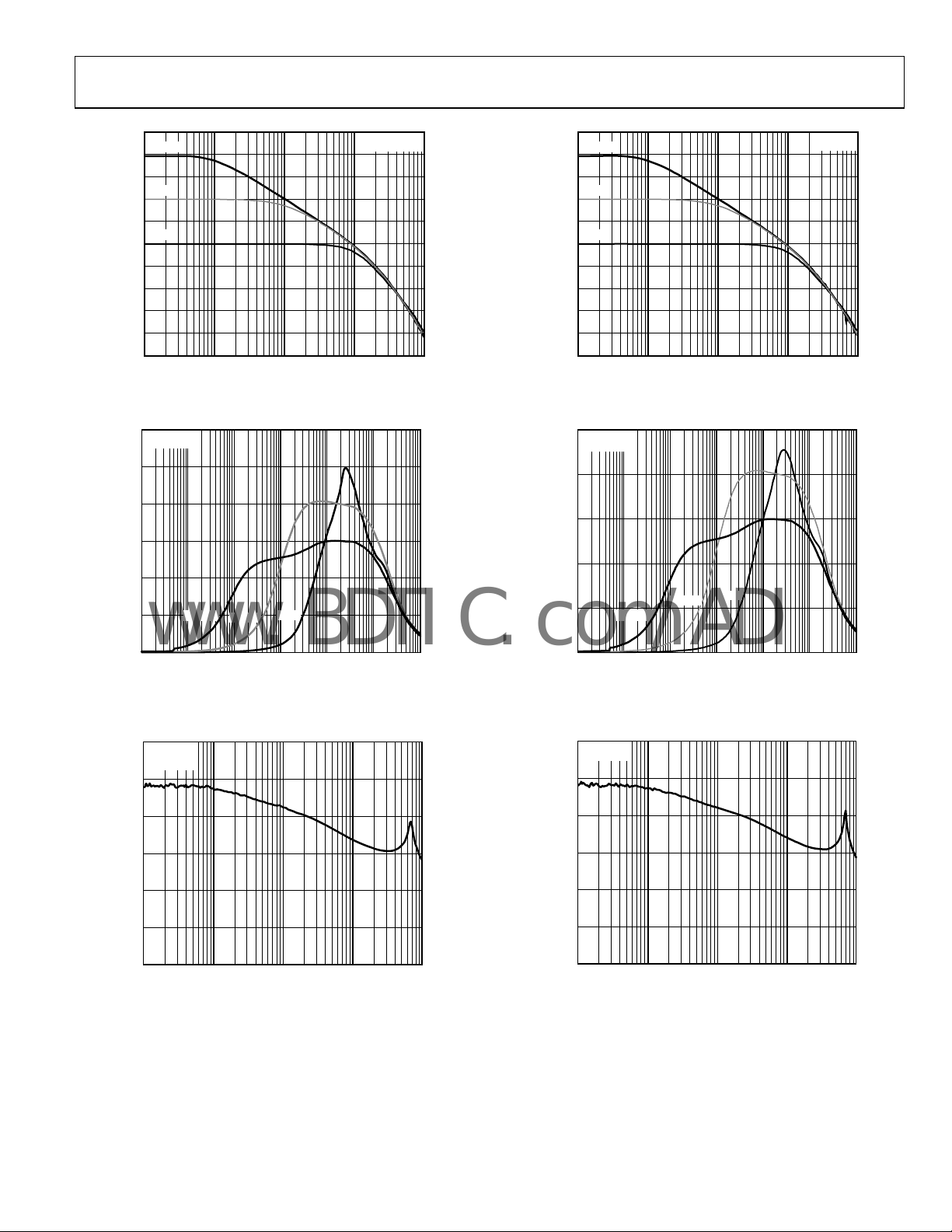
Figure 16. Open-Loop Gain and Phase vs. Frequency
VSY = 1.8V
225
180
135
90
45
0
–45
PHASE (Degrees)
–90
–135
–180
–225
06900-035
Rev. 0 | Page 8 of 12
100
80
60
40
20
0
–20
–40
OPEN-LOOP GAIN (dB)
–60
–80
–100
100 1M100k10k1k
PHASE
GAIN
FREQUENCY (Hz)
Figure 19. Open-Loop Gain and Phase vs. Frequency
VSY = 5V
225
180
135
90
45
0
–45
–90
–135
–180
PHASE (Degrees)
06900-036
Page 9
AD8506
www.BDTIC.com/ADI
50
G=100
40
30
G=10
20
10
G= 1
0
–10
–20
CLOSED-LOOP GAIN (dB)
–30
–40
–50
100 1M
1k 10k 100k
FREQUENCY (Hz)
Figure 20. Closed-Loop Gain vs. Frequency
3000
VSY = 1.8V
2500
2000
(Ω)
1500
OUT
Z
1000
500
G = 100
G = 10
G = 1
VSY = 1.8V
6900-017
50
G = 100
40
30
G = 10
20
10
G = 1
0
–10
–20
CLOSED-LOOP GAIN (dB)
–30
–40
–50
100 1M
1k 10k 100k
FREQUENCY (Hz)
Figure 23. Closed-Loop Gain vs. Frequency
2500
VSY = 5V
2000
1500
(Ω)
OUT
Z
1000
500
G = 100
G = 10
G = 1
VSY = 5V
6900-020
0
10 100 1k 10k 100k 1M 10M
120
VSY = 1.8V
T
= 25°C
A
100
80
60
CMRR (dB)
40
20
0
100 1M100k10k1k
FREQUENCY (Hz)
Figure 21. Z
FREQUENCY (Hz)
vs. Frequency
OUT
Figure 22. CMRR vs. Frequency
0
6900-021
06900-022
10 100 1k 10k 100k 1M 10M
120
VSY = 5V
100
80
60
CMRR (dB)
40
20
0
100 1M100k10k1k
FREQUENCY (Hz)
Figure 24. Z
FREQUENCY (Hz)
vs. Frequency
OUT
6900-024
06900-025
Figure 25. CMRR vs. Frequency
Rev. 0 | Page 9 of 12
Page 10

AD8506
www.BDTIC.com/ADI
100
90
80
70
60
50
PSRR (dB)
40
30
20
10
0
10 100 1k 10k 100k 1M
PSRR–
FREQUENCY (Hz)
VSY = 1.8V
PSRR+
Figure 26. PSRR vs. Frequency
06900-023
100
90
80
70
60
50
PSRR (dB)
40
30
20
10
0
10 100 1k 10k 100k 1M
FREQUENCY (Hz)
PSRR–
PSRR+
Figure 29. PSRR vs. Frequency
VSY = 5V
06900-026
80
VSY = 1.8V
R
= 100kΩ
L
70
60
50
40
30
OVERSHOOT (%)
–OVERSHOO T
20
10
+OVERSHOO T
0
10 1k100
C
LOAD
(pF)
Figure 27. Small Signal Overshoot vs. Load Capacitance
80
VSY = 5V
R
= 100kΩ
L
70
60
50
40
30
OVERSHOOT (%)
06900-027
–OVERSHOO T
20
10
+OVERSHOO T
0
10 1k100
C
LOAD
(pF)
06900-030
Figure 30. Small Signal Overshoot vs. Load Capacitance
VOLTAGE (500mV/DIV)
TIME (100µs/DIV)
VSY = 1.8V
R
= 100kΩ
L
C
= 100pF
L
06900-028
Figure 28. Large Signal Transient Response
VOLTAGE (1V/DIV)
Figure 31. Large Signal Transient Response
Rev. 0 | Page 10 of 12
VSY = 5V
R
C
TIME (100µs/DIV)
= 100kΩ
L
= 100pF
L
06900-031
Page 11

AD8506
www.BDTIC.com/ADI
VOLTAGE (2mV/DIV)
TIME (100µs/DIV)
VSY = 1.8V
R
= 100kΩ
L
C
= 100pF
L
06900-029
VOLTAGE (2mV/DIV)
TIME (100µs/DIV)
VSY = 5V
R
= 100kΩ
L
C
= 100pF
L
06900-032
Figure 32. Small Signal Transient Response Figure 34. Small Signal Transient Response
100
VSY = 5V
10
(nV/ Hz)
N
e
VOLTAGE (0.5µV/DIV)
1
100 1M10k1k
FREQUENCY (Hz)
Figure 33. Voltage Noise Density vs. Frequency
06900-033
Figure 35. Voltage Noise 0.1 Hz to 10 Hz
TIME (4s/ DIV)
VSY = 1.8V AND 5V
2.78µV p-p
06900-034
Rev. 0 | Page 11 of 12
Page 12

AD8506
www.BDTIC.com/ADI
OUTLINE DIMENSIONS
3.20
3.00
2.80
8
5
3.20
3.00
1
2.80
PIN 1
0.65 BSC
0.95
0.85
0.75
0.15
0.38
0.00
0.22
COPLANARITY
0.10
COMPLIANT TO JEDEC STANDARDS MO-187-AA
Figure 36. 8-Lead Mini Small Outline Package [MSOP]
ORDERING GUIDE
Model Temperature Range Package Description Package Option Branding
AD8506ARMZ-R2
AD8506ARMZ-REEL
1
Z = RoHS Compliant Part.
1
–40°C to +125°C 8-Lead Mini Small Outline Package [MSOP] RM-8 A1X
1
–40°C to +125°C 8-Lead Mini Small Outline Package [MSOP] RM-8 A1X
5.15
4.90
4.65
4
1.10 MAX
0.23
SEATING
PLANE
0.08
(RM-8)
Dim
ensions shown in millimeters
8°
0°
0.80
0.60
0.40
©2007 Analog Devices, Inc. All rights reserved. Trademarks and
registered trademarks are the property of their respective owners.
D06900-0-11/07(0)
Rev. 0 | Page 12 of 12
 Loading...