

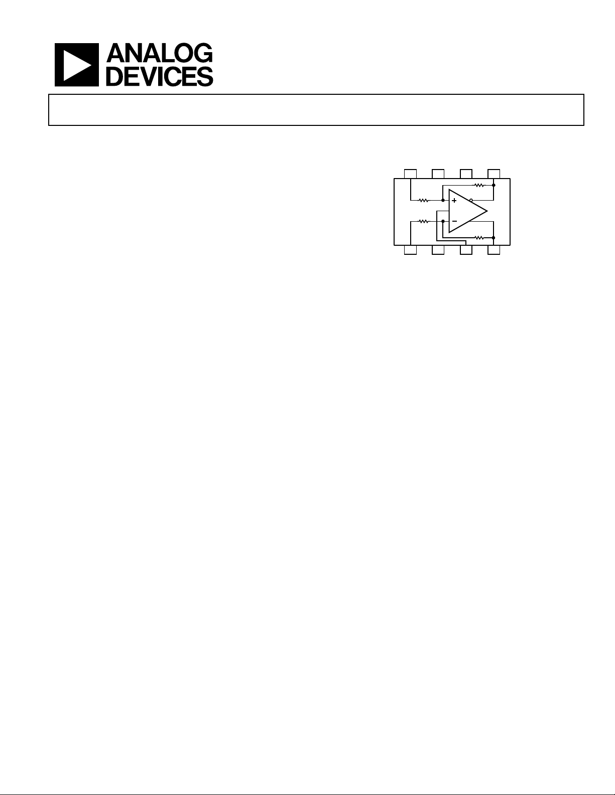
Low Power, Unity Gain, Fully Differential
AD8476
10kΩ
10kΩ
10kΩ
10kΩ
INN
1
+V
S
2
VOCM
3
+OUT
4
INP8–V
S
7
NC
6
–OUT
5
NOTES
1. NC = NO CONNECT .
DO NOT CONNECT TO THIS PIN.
10195-001
AD8476
Data Sheet
FEATURES
Very low power
330 μA supply current
Fully differential or single-ended inputs/outputs
Differential output designed to drive precision ADCs
Drives switched capacitor and Σ-Δ ADCs
Rail-to-rail outputs
VOCM pin adjusts output common mode
Robust overvoltage up to 18 V beyond supplies
High performance
Suitable for driving 16-bit converter up to 250 kSPS
39 nV/√Hz output noise
1 ppm/°C gain drift maximum
200 μV maximum output offset
10 V/μs slew rate
5 MHz bandwidth
Single supply: 3 V to 18 V
Dual supplies: ±1.5 V to ±9 V
Amplifier and ADC Driver
FUNCTIONAL BLOCK DIAGRAM
Figure 1.
APPLICATIONS
ADC driver
Differential instrumentation amplifier building block
Single-ended-to-differential converter
Battery-powered instruments
GENERAL DESCRIPTION
The AD8476 is a very low power, fully differential precision
amplifier with integrated gain resistors for unity gain. It is an ideal
choice for driving low power, high performance ADCs as a
single-ended-to-differential or differential-to-differential
amplifier. It provides a precision gain of 1, common-mode level
shifting, low temperature drift, and rail-to-rail outputs for
maximum dynamic range.
The AD8476 also provides overvoltage protection from large
industrial input voltages up to ±23 V while operating on a dual 5 V
supply. Power dissipation on a single 5 V supply is only 1.5 mW.
The AD8476 works well with SAR, Σ-Δ, and pipeline converters.
The high current output stage of the part allows it to drive the
switched capacitor front-end circuits of many ADCs with
minimal error.
Unlike many differential drivers on the market, the AD8476 is
a high precision amplifier. With 200 µV maximum output
offset, 39 nV/√Hz noise, and −102 dB THD + N at 10 kHz, the
AD8476 pairs well with low power, high accuracy converters.
Considering its low power consumption and high precision, the
slew-enhanced AD8476 has excellent speed, settling to 16-bit
precision for 250 kSPS acquisition times.
The AD8476 is available in a space-saving 8-lead MSOP
package. It is fully specified over the −40°C to +125°C
temperature range.
Rev. A
Information furnished by Analog Devices is believed to be accurate and reliable. However, no
responsibility is assumed by Analog Devices for its use, nor for any infringements of patents or other
rights of third parties that may result from its use. Specifications subject to change without n otice. No
license is granted by implication or otherwise under any patent or patent rights of Analog Devices.
Trademarks and registered trademarks are the property of their respective owners.
One Technology Way, P.O. Box 9106, Norwood, MA 02062-9106, U.S.A.
Tel: 781.329.4700
Fax: 781.461.3113 ©2011 Analog Devices, Inc. All rights reserved.
www.analog.com

AD8476 Data Sheet
TABLE OF CONTENTS
Features .............................................................................................. 1
Applications ....................................................................................... 1
Functional Block Diagram .............................................................. 1
General Description ........................................................................... 1
Revision History ............................................................................... 2
Specifications ..................................................................................... 3
Absolute Maximum Ratings ............................................................ 5
Thermal Resistance ...................................................................... 5
Maximum Power Dissipation ..................................................... 5
ESD Caution .................................................................................. 5
Pin Configuration and Function Descriptions ............................. 6
Typical Performance Characteristics ............................................. 7
Terminology .................................................................................... 15
REVISION HISTORY
11/11—Rev. 0 to Rev. A
Changes to Table 1 ............................................................................ 3
Changes to Typical Performance Characteristics ......................... 7
Added Figure 39; Renumbered Sequentially .............................. 13
Added Table 5 .................................................................................. 18
Removed Low Power ADC Driving Section ............................... 19
Removed Figure 52 ......................................................................... 19
10/11—Revision 0: Initial Version
Theory of Operation ...................................................................... 16
Overview ..................................................................................... 16
Circuit Information .................................................................... 16
DC Precision ............................................................................... 16
Input Voltage Range ................................................................... 17
Driving the AD8476................................................................... 17
Power Supplies ............................................................................ 17
Applications Information .............................................................. 18
Typical Configuration ................................................................ 18
Single-Ended-to-Differential Conversion ............................... 18
Setting the Output Common-Mode Voltage .......................... 18
Outline Dimensions ....................................................................... 19
Ordering Guide .......................................................................... 19
Rev. A | Page 2 of 20

Data Sheet AD8476
SPECIFICATIONS
VS = +5 to ±5 V, VOCM = midsupply, V
otherwise noted.
Table 1.
Parameter Test Conditions/Comments
DYNAMIC PERFORMANCE
−3 dB Small Signal Bandwidth V
−3 dB Large Signal Bandwidth V
Slew Rate V
Settling Time to 0.01% V
Settling Time to 0.001% V
NOISE/DISTORTION1
THD + N f = 10 kHz, V
HD2 f = 10 kHz, V
HD3 f = 10 kHz, V
IMD3 f1 = 95 kHz, f2 = 105 kHz,
Output Voltage Noise f = 0.1 Hz to 10 Hz 6 6 µV p-p
Spectral Noise Density f = 10 kHz 39 39 nV/√Hz
GAIN 1 1 V/V
Gain Error RL = ∞ 0.02 0.04 %
Gain Drift −40°C ≤ TA ≤ +125°C 1 1 ppm/°C
Gain Nonlinearity V
OFFSET AND CMRR
Differential Offset2 50 200 50 500 µV
vs. Temperature −40°C ≤ TA ≤ +125°C 900 900 µV
Average TC −40°C ≤ TA ≤ +125°C 1 4 1 4 µV/°C
vs. Power Supply (PSRR) VS = ±2.5 V to ±9 V 90 90 dB
Common-Mode Offset2 50 50 µV
Common-Mode Rejection
Ratio
INPUT CHARACTERISTICS
Input Voltage Range3 Differential input −VS + 0.05 +VS − 0.05 −VS + 0.05 +VS − 0.05 V
Single-ended input 2(−VS + 0.05) 2(+V − 0.05) 2(−VS + 0.05)
Impedance4 Vcm = VS/2
Single-Ended Input 13.3 13.3 kΩ
Differential Input 20 20 kΩ
Common-Mode Input 10 10 kΩ
OUTPUT CHARACTERISTICS
Output Swing VS = +5 V −VS + 0.125 +VS − 0.14 −VS + 0.125 +VS − 0.14
VS = ±5 V −VS + 0.155 +VS − 0.18 −VS + 0.155 +VS − 0.18
Output Balance Error ∆V
Output Impedance 0.1 0.1 Ω
Capacitive Load Per output 20 20 pF
Short-Circuit Current Limit 35 35 mA
VOCM CHARACTERISTICS
VOCM Input Voltage Range −VS + 1 +VS − 1 −VS + 1 +VS − 1 V
VOCM Input Impedance 500 500 kΩ
VOCM Gain Error 0.05 0.05 %
22 kHz filter
V
V
OUT
= V
+OUT
− V
, RL = 2 kΩ differential, referred to output (RTO), TA = 25°C, unless
−OUT
B Grade A Grade
= 200 mV p-p 5 5 MHz
OUT
= 2 V p-p 1 1 MHz
OUT
= 2 V step 10 10 V/µs
OUT
= 2 V step 1.0 1.0 µs
OUT
= 2 V step 1.6 1.6 µs
OUT
= 2 V p-p,
OUT
= 2 V p-p −120 −120 dB
OUT
= 2 V p-p −122 −122 dB
OUT
−102 −102 dB
−82 −82 dBc
= 2 V p-p
OUT
= 4 V p-p 5 5 ppm
OUT
= ±5 V 90 80 dB
IN,cm
2(+VS − 0.05)
/∆V
OUT,cm
90 80 dB
OUT,dm
Unit Min Typ Max Min Typ Max
V
Rev. A | Page 3 of 20

AD8476 Data Sheet
B Grade A Grade
Parameter Test Conditions/Comments
POWER SUPPLY
Specified Supply Voltage ±5 ±5 V
Operating Supply Voltage
3 18 3 18 V
Range
Supply Current VS = +5 V, TA = 25°C 300 330 300 330 μA
VS = ±5 V, TA = 25°C 330 380 330 380 μA
Over Temperature −40°C ≤ TA ≤ +125°C 400 500 400 500 μA
TEMPERATURE RANGE
Specified Performance Range −40 +125 −40 +125 °C
1
Includes amplifier voltage and current noise, as well as noise of internal resistors.
2
Includes input bias and offset current errors.
3
The input voltage range is a function of the voltage supplies and ESD dio des.
4
Internal resistors are trimmed to be r atio matched but have ±20% absolute accuracy.
Unit Min Typ Max Min Typ Max
Rev. A | Page 4 of 20
Data Sheet AD8476
ABSOLUTE MAXIMUM RATINGS
Table 2.
Parameter Rating
Supply Voltage ±10 V
Maximum Voltage at Any Input Pin +VS + 18 V
Minimum Voltage at Any Input Pin −VS – 18 V
Storage Temperature Range −65°C to +150°C
Specified Temperature Range −40°C to +125°C
Package Glass Transition Temperature (TG) 150°C
ESD (Human Body Model) 2500 V
Stresses above those listed under Absolute Maximum Ratings
may cause permanent damage to the device. This is a stress
rating only; functional operation of the device at these or any
other conditions above those indicated in the operational
section of this specification is not implied. Exposure to absolute
maximum rating conditions for extended periods may affect
device reliability.
THERMAL RESISTANCE
The θJA values in Table 3 assume a 4-layer JEDEC standard
board with zero airflow.
Table 3. Thermal Resistance
Package Type θJA Unit
8-Lead MSOP 209.0 °C/W
MAXIMUM POWER DISSIPATION
The maximum safe power dissipation for the AD8476 is limited
by the associated rise in junction temperature (T
approximately 150°C, which is the glass transition temperature,
the properties of the plastic change. Even temporarily exceeding
this temperature limit may change the stresses that the package
exerts on the die, permanently shifting the parametric performance
of the amplifiers. Exceeding a temperature of 150°C for an
extended period may result in a loss of functionality.
) on the die. At
J
ESD CAUTION
Rev. A | Page 5 of 20
AD8476 Data Sheet
INN
1
+V
S
2
VOCM
3
+OUT
4
INP
8
–V
S
7
NC
6
–OUT
5
AD8476
TOP VIEW
(Not to S cale)
NOTES
1. NC = NO CONNECT.
DO NOT CO NNE CT TO THIS PIN.
10195-004
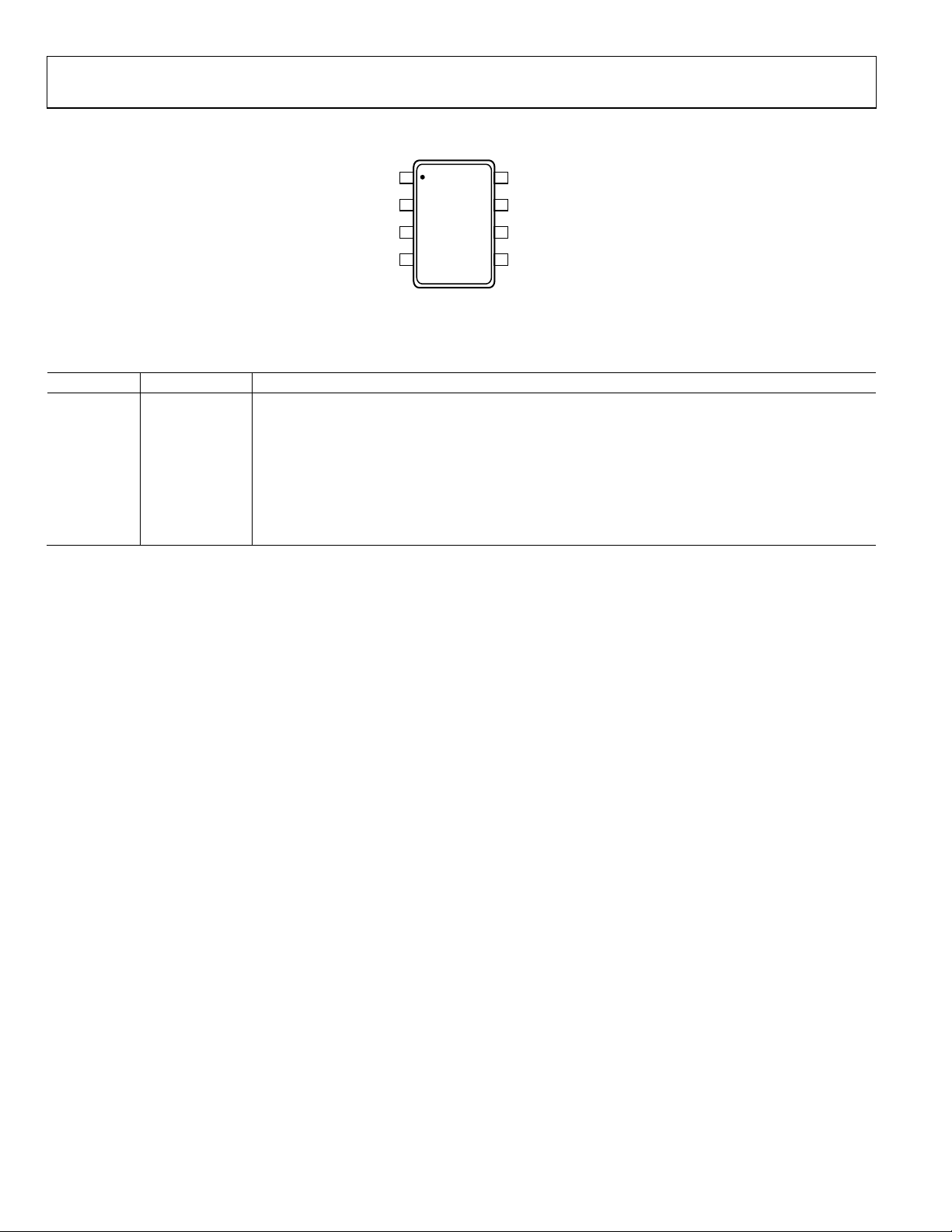
PIN CONFIGURATION AND FUNCTION DESCRIPTIONS
Figure 2. 8-Lead MSOP Pin Configuration
Table 4. 8-Lead MSOP Pin Function Descriptions
Pin No. Mnemonic Description
1 INN Negative Input .
2 +VS Positive Supply.
3 VOCM Output Common-Mode Adjust.
4 +OUT Noninverting Output.
5 −OUT Inverting Output.
6 NC No Connect.
7 −VS Negative Supply.
8 INP Positive Input.
Rev. A | Page 6 of 20

Data Sheet AD8476
50
–50
–40
–30
–20
–10
0
10
20
30
40
–40 –25 –10 5 20 35 50 65 80 95 110 125
CMRR (µV/V)
TEMPERATURE (°C)
10195-005
NORMALIZED TO 25° C
–40 –25 –10 5 20 35 50 65 80 95 110 125
OFFSET VOLTAGE (µV)
TEMPERATURE (°C)
10195-006
–1500
–1300
–1100
–900
–700
–500
–300
–100
100
300
500
700
900
1100
1300
1500
NORMALIZED TO 25° C
–40 –25 –10 5 20 35 50 65 80 95 110 125
GAIN ERROR ( µ V /V)
TEMPERATURE (°C)
10195-007
–150
–100
–50
0
50
100
150
NORMALIZED TO 25° C
15
–15
–10
–5
0
5
10
–15 –10 –5 0 5 10 15
COMMON-MODE VOLTAGE (V)
OUTPUT VOLTAGE (V)
10195-008
V
S
= ±5V
V
S
= ±2.5V
115
65
70
75
80
85
90
95
100
105
110
10 100 1k 10k 100k 1M
CMRR (dB)
FREQUENCY (Hz)
V
S
= ±5V
V
S
= +5V
10195-010
–20
–100
–90
–80
–70
–60
–50
–40
–30
100 1k 10k 100k 1M 10M
PSRR (dB)
FREQUENCY ( Hz )
10195-011
VS = ±5V
VS = +5V
TYPICAL PERFORMANCE CHARACTERISTICS
VS = +5 V, G = 1, VOCM connected to 2.5 V, RL = 2 kΩ differentially, TA = 25°C, referred to output (RTO), unless otherwise noted.
Figure 3. CMRR vs. Temperature
Figure 4. System Offset Temperature Drift
Figure 6. Input Common-Mode Voltage vs. Output Voltage,
V
= ±5 V and ±2.5 V
S
Figure 7. Common-Mode Rejection vs. Frequency
Figure 5. Gain Error vs. Temperature
Figure 8. Power Supply Rejection vs. Frequency
Rev. A | Page 7 of 20

AD8476 Data Sheet
20
18
16
14
12
10
8
6
4
2
0
100 1k 10k 100k 10M1M
MAXIMUM OUTPUT VOLTAGE (V p-p)
FREQUENCY ( Hz )
2kΩ LOAD
NO LOAD
10195-012
1k 10k 100k 1M
OUTPUT VOLTAGE SWING (V)
REFERRED TO SUPPLY VOLTAGES
R
LOAD
(Ω)
10195-013
–55°C
–40°C
+25°C
+85°C
+125°C
+V
S
0.050
0.025
0.075
0.100
0.125
–V
S
0.025
0.050
0.075
0.100
0.125
0.150
0.175
0.150
0.175
–40 –25 –10 5 20 35 50 65 80 95 110 125
SLEW RATE (V/µS)
TEMPERATURE (°C)
10195-015
15
5
6
7
8
9
10
11
12
13
14
RISE
FALL
–40 –25 –10 5 20 35 50 65 80 95 110 125
CURRENT (mA)
TEMPERATURE (°C)
10195-016
50
5
10
15
20
25
30
35
40
45
V
S
= ±5V
V
S
= ±2.5V
10µA 100µA 1mA 10mA
OUTPUT VOLTAGE SWING (V)
REFERRED TO SUPPLY VOLTAGES
CURRENT (A)
10195-014
+V
S
0.050
0.025
0.075
0.100
0.125
–V
S
0.025
0.050
0.075
0.100
0.125
0.150
0.175
0.150
0.175
+125°C
+85°C
+25°C
–40°C
–55°C
2V/DIV
2µs/DIV
10195-051
V
IN
V
OUT
Figure 9. Maximum Output Voltage vs. Frequency
Figure 10. Output Voltage Swing vs. R
LOAD
vs. Temperature, VS = ±5 V
Figure 12. Short-Circuit Current vs. Temperature
Figure 13. Output Voltage Swing vs. Load Current vs. Temperature,
V
= ±5 V
S
Figure 11. Slew Rate vs. Temperature
Figure 14. Overdrive Recovery, V
= +5 V
S
Rev. A | Page 8 of 20

Data Sheet AD8476
10
–50
–45
–40
–35
–30
–25
–20
–15
–10
–5
0
5
100 1k 10k 100k 1M 10M
GAIN (dB)
FREQUENCY (Hz)
VS = ±5V
V
S
= +5V
10195-017
10
–50
–45
–40
–35
–30
–25
–20
–15
–10
–5
0
5
100 1k 10k 100k 1M 10M
GAIN (dB)
FREQUENCY (Hz)
R
L
= 10kΩ
RL = 2kΩ
R
L
= 200Ω
10195-018
10
–50
–40
–30
–20
–10
0
1k 10k 100k 1M 10M 100M
OUTPUT M AGNITUDE (d B)
FREQUENCY ( Hz )
10195-019
CL = 5pF
CL = 10pF
CL = 15pF
10
–50
–45
–40
–35
–30
–25
–20
–15
–10
–5
0
5
100 1k 10k 100k 1M 10M
GAIN (dB)
FREQUENCY (Hz)
VS = ±5V
VS = +5V
10195-020
10
–40
–35
–30
–25
–20
–15
–10
–5
0
5
100 1k 10k 100k 1M 10M
OUTPUT M AGNITUDE (d B)
FREQUENCY (Hz)
RL = 10kΩ
RL = 2kΩ
RL = 200Ω
10195-021
10
–40
–35
–30
–25
–20
–15
–10
–5
0
5
100 1k 10k 100k 1M 10M
OUTPUT M AGNITUDE (d B)
FREQUENCY ( Hz )
10195-101
CL = 5pF
CL = 10pF
CL = 15pF
Figure 15. Small Signal Frequency Response for Various Supplies
Figure 16. Small Signal Frequency Response for Various Loads
Figure 18. Large Signal Frequency Response for Various Supplies
Figure 19. Large Signal Frequency Response for Various Loads
Figure 17. Small Signal Frequency Response for Various Capacitive Loads
Figure 20. Large Signal Frequency Response for Various Capacitive Loads
Rev. A | Page 9 of 20

AD8476 Data Sheet
5
–25
–20
–15
–10
–5
0
1k 10k 100k 1M 10M
OUTPUT M AGNITUDE (d B)
FREQUENCY ( Hz )
VOCM = 1.0V
VOCM = 2.5V
VOCM = 4.0V
10195-024
5
–30
–25
–20
–15
–10
–5
0
1k 100k10k 1M 10M
OUTPUT M AGNITUDE (d B)
VOCM INPUT FREQUENCY ( Hz )
10195-056
POSITIVE OUTPUT (2kΩ LOAD) V
S
= 5V
NEGATIVE OUTPUT (2kΩ LOAD)
50mV/DIV
500ns/DIV
VS = ±5V
VS = +5V
VS = +3V
10195-029
5
–35
–20
–25
–30
–15
–10
–5
0
1k 10k 100k 1M 10M
OUTPUT M AGNITUDE (d B)
FREQUENCY (Hz)
CL = 5pF
CL = 10pF
CL = 15pF
10195-027
5
–30
–25
–20
–15
–10
–5
0
1k 100k10k 1M
OUTPUT M AGNITUDE (d B)
VOCM INPUT FREQUENCY ( Hz )
10195-055
POSITIVE OUTPUT
NEGATIVE OUTPUT
500mV/DIV
500ns/DIV
10195-032
VS = ±5V
VS = +5V
VS = +3V
Figure 21. Small Signal Frequency Response for Various VOCM Levels
Figure 22. VOCM Small Signal Frequency Response
Figure 24. Large Signal Frequency Response for Various VOCM Level
Figure 25. VOCM Large Signal Frequency Response
Figure 23. Small Signal Pulse Response for Various Supplies
Figure 26. Large Signal Pulse Response for Various Supplies
Rev. A | Page 10 of 20

Data Sheet AD8476
50mV/DIV
500ns/DIV
R
L
= 10kΩ
R
L
= 2kΩ
RL = 200Ω
10195-030
50mV/DIV
500ns/DIV
CL = 0pF
C
L
= 5pF
C
L
= 10pF
10195-031
20mV/DIV
500ns/DIV
10195-035
500mV/DIV
500ns/DIV
RL = 10kΩ
RL = 2kΩ
RL = 200Ω
10195-033
500mV/DIV
500ns/DIV
C
L
= 0pF
CL = 5pF
CL = 10pF
10195-034
500mV/DIV
10µs/DIV
10195-038
Figure 27. Small Signal Step Response for Various Resistive Loads, V
Figure 28. Small Signal Step Response for Various Capacitive Loads, V
= ±5 V
S
= ±5 V
S
Figure 30. Large Signal Step Response for Various Resistive Loads, V
Figure 31. Large Signal Step Response for Various Capacitive Loads, V
= ±5 V
S
= ±5 V
S
Figure 29. VOCM Small Signal Step Response
Figure 32. VOCM Large Signal Step Response
Rev. A | Page 11 of 20

AD8476 Data Sheet
3.0
–3.0
–2.5
–2.0
–1.5
–1.0
–0.5
0
0.5
1.0
1.5
2.0
2.5
0 100908070605040302010
OUTPUT VOLTAGE (µV)
TIME (Seconds)
10195-039
–20
–30
–40
–50
–60
–70
–80
–90
–100
–110
–120
–130
–140
100 1k 10k 100k 1M
HARMONIC DIS TORTIO N ( dBc)
FREQUENCY ( Hz )
10195-040
HD2, R
L
= NO LOAD
HD3, R
L
= NO LOAD
HD2, RL = 2kΩ LOAD
HD3, R
L
= 2kΩ LOAD
–30
–40
–50
–60
–70
–80
–90
–100
–110
–120
–130
–140
100 1k
10k 100k 1M
HARMONIC DIS TORTIO N ( dBc)
FREQUENCY ( Hz )
10195-042
HD2 (V
S
= ±5V, RL = 2kΩ)
HD3 (VS = ±5V, R
L
= 2kΩ)
HD2 (VS = +5V, R
L
= 2kΩ)
HD3 (VS = +5V, R
L
= 2kΩ)
140
130
120
110
100
90
80
70
60
50
40
30
20
1 10 100 1k 10k 100k
SPECTRAL NOISE DENSITY (nV/ Hz)
FREQUENCY ( Hz )
10195-036
–20
–30
–40
–50
–60
–70
–80
–90
–100
–110
–120
–130
–140
100 1k 10k 100k 1M
HARMONIC DIS TORTIO N ( dBc)
FREQUENCY ( Hz )
10195-046
HD2 (V
OUT
= 4V p-p)
HD3 (V
OUT
= 4V p-p)
HD2 (V
OUT
= 2V p-p)
HD3 (V
OUT
= 2V p-p)
–20
–30
–40
–50
–60
–70
–80
–90
–100
–110
–120
–130
–140
0 1 2 3 4 5 6 7 8 9 10
HARMONIC DIS TORTIO N ( dBc)
V
OUT
(V p-p)
10195-047
HD2, V
S
= 5V
HD3, VS = 5V
Figure 33. 0.1 Hz to 10 Hz Voltage Noise
Figure 34. Harmonic Distortion vs. Frequency at Various Loads
Figure 36. Voltage Noise Density vs. Frequency
Figure 37. Harmonic Distortion vs. Frequency at Various V
OUT,dm
Figure 35. Harmonic Distortion vs. Frequency at Various Supplies
Figure 38. Harmonic Distortion vs. V
OUT,dm
, f = 10 kHz
Rev. A | Page 12 of 20

Data Sheet AD8476
–140
–130
–120
–110
–100
–90
–80
–70
–60
–50
–40
–30
–20
–10
0
100 1k 10k 100k 1M
HARMONIC DISTORTION (dBc)
FREQUENCY (Hz)
HD2 (SINGL E - E NDE D INPUT)
HD3 (SINGL E - E NDE D INPUT)
HD2 (DIFFE RE NTIAL I NP UT)
HD3 (DIFFE RE NTIAL I NP UT)
10195-139
–80
–120
–115
–110
–105
–100
–95
–90
–85
10 1k100 10k 100k
THD + N (dB)
FREQUENCY ( Hz )
10195-053
V
OUT
= 2V p-p
V
OUT
= 4V p-p
V
OUT
= 8V p-p
1µs/DIV
10195-037
1V/DIV
200µV/DIV
0.01%/DIV
40
–40
–35
–30
–25
–20
–15
–10
–5
0
5
10
15
20
25
30
35
–1.0 –0.8 –0.6 –0.4 –0.2 0 0.2 0.4 0.6 0.8 1.0
ERROR (pp m)
OUTPUT VOLTAGE (V)
10195-200
VS = ±5V
–20
–30
–40
–50
–60
–70
–80
–90
–100
–110
–120
–130
–140
100 1k 10k 100k 1M
SPURIOUS- FREE DYNAMCI C RANGE (dBc)
FREQUENCY ( Hz )
10195-049
VS = 5V, RL = 2kΩ
VS = 5V, RL = NO LOAD
2µs/DIV
10195-100
1V/DIV
20µV/DIV
0.001%/DIV
Figure 39. Harmonic Distortion vs. Input Drive
Figure 40. Total Harmonic Distortion + Noise vs. Frequency
Figure 42. Gain Nonlinearity
Figure 43. Spurious-Free Dynamic Range vs. Frequency at Various Loads
Figure 41. Settling Time to 0.01% of 2 V Step
Figure 44. Settling Time to 0.001% of 2 V Step
Rev. A | Page 13 of 20

AD8476 Data Sheet
–30
–40
–50
–60
–70
–80
–90
–100
100 1k 10k 100k 1M 10M
OUTPUT BALANCE ERROR (dB)
FREQUENCY ( Hz )
10195-050
10
–100
–90
–80
–70
–60
–50
–40
–30
–20
–10
0
80 10090 110 1209585 105 115
NORMALIZED SPECT RUM ( dBc)
FREQUENCY ( Hz )
10195-054
1k
100
10
1
0.1
10k 100k 1M 10M
IMPEDANCE (Ω)
FREQUENCY ( Hz )
10195-052
POSITIVE OUTPUT
NEGATIVE OUTPUT
Figure 45. Output Balance Error vs. Frequency
Figure 47. Output Impedance vs. Frequency
Figure 46. 100 kHz Intermodulation Distortion
Rev. A | Page 14 of 20

Data Sheet AD8476
+IN
VOCM
–IN
+OUT
–OUT
V
OUT, dm
R
L, dm
AD8476
10kΩ
10kΩ
10kΩ
10kΩ
10195-057
dmOUT
cmOUT
V
V
ErrorBalanceOutput
,
,
∆
∆
=
TERMINOLOGY
Common-Mode Voltage
Common-mode voltage refers to the average of two node voltages
with respect to the local ground reference. The output commonmode voltage is defined as
V
Figure 48. Signal and Circuit Definitions
Differential Voltage
Differential voltage refers to the difference between two
node voltages. For example, the output differential voltage (or
equivalently, output differential mode voltage) is defined as
V
where V
OUT, dm
+OUT
= (V
and V
+OUT
− V
−OUT
)
−OUT
refer to the voltages at the +OUT and
−OUT terminals with respect to a common ground reference.
Similarly, the differential input voltage is defined as
V
= (V
− V
IN, dm
+IN
−IN
)
= (V
OUT, cm
Balance
Output balance is a measure of how close the output differential
signals are to being equal in amplitude and opposite in phase.
Output balance is most easily determined by placing a wellmatched resistor divider between the differential voltage nodes
and comparing the magnitude of the signal at the divider midpoint
with the magnitude of the differential signal. By this definition,
output balance is the magnitude of the output common-mode
voltage divided by the magnitude of the output differential
mode voltage.
+OUT
+ V
−OUT
)/2
Rev. A | Page 15 of 20

AD8476 Data Sheet
10kΩ
10kΩ
10kΩ
10kΩ
INN
1
+V
S
2
VOCM
3
+OUT
4
INP
8
–V
S
7
NC
6
–OUT
5
NOTES
1. NC = NO CONNECT.
DO NOT CO NNE CT TO THIS PIN.
10195-058
AD8476
( )
( )
( )
( )
NP
dmOUT
NP
cmOUT
NPNP
dmIN
NPcmIN
RRVRRV
RRRRVRRV
+++−=
+++−
2
2
1
2
2
1
,
,
,
,
RGP
RFP
R
P
=
RGN
RFN
R
N
=
−=
)(
2
1
, NPcmIN
VVV +=
NP
NPNP
dmIN
dmOUT
RR
RRRR
V
V
++
++
=
2
2
,
,
( )
NP
NP
cmIN
dmOUT
RR
RR
V
V
++
−
=
2
2
,
,
RFP
RFN
RGP
RGN
V
ON
V
OP
VOCM
V
P
V
N
10195-059
RG
RF
v
v
dmIN
dmOUT
=
,
,
THEORY OF OPERATION
OVERVIEW
The AD8476 is a fully differential amplifier, with integrated lasertrimmed resistors, that provides a precision gain of 1. The
internal differential amplifier of the AD8476 differs from
conventional operational amplifiers in that it has two outputs
whose voltages are equal in magnitude, but move in opposite
directions (180° out of phase).
The AD8476 is designed to greatly simplify single-ended-todifferential conversion, common-mode level shifting and
precision driving of differential signals into low power,
differential input ADCs. The VOCM input allows the user to
set the output common-mode voltage to match with the input
range of the ADC. Like an operational amplifier, the VOCM
function relies on high open-loop gain and negative feedback to
force the output nodes to the desired voltages.
Due to the internal common-mode feedback loop and the fully
differential topology of the amplifier, the AD8476 outputs are
precisely balanced over a wide frequency range. This means that
the amplifier’s differential outputs are very close to the ideal of
being identical in amplitude and exactly 180° out of phase.
DC PRECISION
The dc precision of the AD8476 is highly dependent on the
accuracy of its integrated gain resistors. Using superposition to
analyze the circuit shown in Figure 50, the following equation
shows the relationship between the input and output voltages of
the amplifier:
where:
CIRCUIT INFORMATION
The AD8476 amplifier uses a voltage feedback topology;
therefore, the amplifier exhibits a nominally constant gain
bandwidth product. Like a voltage feedback operational
amplifier, the AD8476 also has high input impedance at its
internal input terminals (the summing nodes of the internal
amplifier) and low output impedance.
The AD8476 employs two feedback loops, one each to control
the differential and common-mode output voltages. The differential feedback loop, which is fixed with precision laser-trimmed
on-chip resistors, controls the differential output voltage.
Output Common-Mode Voltage (VOCM)
The internal common-mode feedback controls the commonmode output voltage. This architecture makes it easy for the
user to set the output common-mode level to any arbitrary
value independent of the input voltage. The output commonmode voltage is forced by the internal common-mode feedback
loop to be equal to the voltage applied to the VOCM input. The
VOCM pin can be left unconnected, and the output commonmode voltage self-biases to midsupply by the internal feedback
control.
Figure 49. Block Diagram
,
VVV
,
dmIN
NP
The differential closed-loop gain of the amplifier is
and the common rejection of the amplifier is
Figure 50. Functional Circuit Diagram of the AD8476 at a Given Gain
The preceding equations show that the gain accuracy and the
common-mode rejection (CMRR) of the AD8476 are determined primarily by the matching of the feedback networks
(resistor ratios). If the two networks are perfectly matched, that
is, if R
and RN equal RF/RG, then the resistor network does not
P
generate any CMRR errors and the differential closed loop gain
of the amplifier reduces to
Rev. A | Page 16 of 20

Data Sheet AD8476
+
+
==
P
MINUSPLUS
V
RG
RF
VOCM
RGRF
RG
VV
2
1
RF
RF
RG
RG
V
ON
V
OP
VOCM
V
P
V
N
V
N
RF + RG
RF
V
P
− V
N
RG
RF
VOCM
RF + RG
RG
+
+
2
1
10195-060
The AD8476 integrated resistors are precision wafer-lasertrimmed to guarantee a minimum CMRR of 90 dB (32 μV/V),
and gain error of less that 0.02%. To achieve equivalent precision
and performance using a discrete solution, resistors must be
matched to 0.01% or better.
INPUT VOLTAGE RANGE
The AD8476 can measure input voltages as large as the supply
rails. The internal gain and feedback resistors form a divider,
which reduces the input voltage seen by the internal input
nodes of the amplifier. The largest voltage that can be measured
properly is constrained by the output range of the amplifier and
the capability of the amplifier’s internal summing nodes. This
voltage is defined by the input voltage, and the ratio between the
feedback and the gain resistors.
Figure 51 shows the voltage at the internal summing nodes of
the amplifier, defined by the input voltage and internal resistor
network. If V
The internal amplifier of the AD8476 has rail-to-rail inputs.
To obtain accurate measurements with minimal distortion, the
voltage at the internal inputs of the amplifier must stay below
+V
− 1 V and above −VS.
S
The AD8476 provides overvoltage protection for excessive input
voltages beyond the supply rails. Integrated ESD protection diodes
is grounded, the expression shown reduces to
N
at the inputs prevent damage to the AD8476 up to +V
and −V
− 18 V.
S
+ 18 V
S
DRIVING THE AD8476
Care should be taken to drive the AD8476 with a low
impedance source: for example, another amplifier. Source
resistance can unbalance the resistor ratios and, therefore,
significantly degrade the gain accuracy and common-mode
rejection of the AD8476. For the best performance, source
impedance to the AD8476 input terminals should be kept
below 0.1 Ω. Refer to the DC Precision section for details on
the critical role of resistor ratios in the precision of the AD8476.
POWER SUPPLIES
The AD8476 operates over a wide range of supply voltages. It
can be powered on a single supply as low as 3 V and as high as
18 V. The AD8476 can also operate on dual supplies from
±1.5 V to ±9 V
A stable dc voltage should be used to power the AD8476. Note
that noise on the supply pins can adversely affect performance.
For more information, see the PSRR performance curve in
Figure 8.
Place a bypass capacitor of 0.1 μF between each supply pin and
ground, as close as possible to each supply pin. Use a tantalum
capacitor of 10 μF between each supply and ground. It can be
farther away from the supply pins and, typically, it can be
shared by other precision integrated circuits.
Figure 51. Voltages at the Internal Op Amp Inputs of the AD8476
Rev. A | Page 17 of 20

AD8476 Data Sheet
10195-102
10kΩ
10kΩ
10kΩ
10kΩ
INN
1
+V
S
2
VOCM
3
+OUT
4
INP
8
–V
S
7
NC6–OUT
5
AD8476
LOAD
INPUT
SIGNAL
SOURCE
+5V
–V
OUT
+V
OUT
+
10µF
0.1µF
+
10µF
0.1µF
–5V
APPLICATIONS INFORMATION
TYPICAL CONFIGURATION
The AD8476 is designed to facilitate single-ended-to-differential
conversion, common-mode level shifting, and precision processing
of signals so that they are compatible with low voltage ADCs.
Figure 52 shows a typical connection diagram of the AD8476.
SINGLE-ENDED-TO-DIFFERENTIAL CONVERSION
Many industrial systems have single-ended inputs from input
sensors; however, the signals are frequently processed by high
performance differential input ADCs for higher precision. The
AD8476 performs the critical function of precisely converting
single-ended signals to the differential inputs of precision
ADCs, and it does so with no need for external components.
To convert a single-ended signal to a differential signal, connect
one input to the signal source and the other input to ground (see
Figure 52). Note that either input can be driven by the source
with the only effect being that the outputs have reversed polarity.
The AD8476 also accepts truly differential input signals in
precision systems with differential signal paths.
SETTING THE OUTPUT COMMON-MODE VOLTAGE
The VOCM pin of the AD8476 is internally biased by a
precision voltage divider comprising of two 1 MΩ resistors
between the supplies. This divider level shifts the output to
midsupply. Relying on the internal bias results in an output
common-mode voltage that is within 0.05% of the expected
value.
In cases where control of the output common-mode level is
desired, an external source or resistor divider can be used to
drive the VOCM pin. If driven directly from a source, or with a
resistor divider of unequal resistor values, the resistance seen by
the VOCM pin should be less than 1 kΩ. If an external voltage
divider consisting of equal resistor values is used to set VOCM
to midsupply, higher values can be used because the external
resistors are placed in parallel with the internal resistors. The
output common-mode offset listed in the Specifications section
assumes that the VOCM input is driven by a low impedance
voltage source.
Because of the internal divider, the VOCM pin sources and sinks
current, depending on the externally applied voltage and its
associated source resistance.
It is also possible to connect the VOCM input to the commonmode level output of an ADC; however, care must be taken to
ensure that the output has sufficient drive capability. The input
impedance of the VOCM pin is 500 kΩ. If multiple AD8476
devices share one ADC reference output, a buffer may be necessary to drive the parallel inputs.
Table 5. Differential Input ADCs
1
ADC Resolution Throughput Rate Power Dissipation
AD7674 16 Bits 100 kSPS 25 mW
AD7684 16 Bits 100 kSPS 6 mW
AD7687 16 Bits 250 kSPS 12.5 mW
AD7688 16 Bits 500 kSPS* 21.5 mW
1
Depending on measurement/application type, check that the AD8476 meets
settling time requirements.
Figure 52. Typical Configuration—8-Lead MSOP
Rev. A | Page 18 of 20

Data Sheet AD8476
COMPLIANT TO JEDEC STANDARDS MO-187-AA
6°
0°
0.80
0.55
0.40
4
8
1
5
0.65 BSC
0.40
0.25
1.10 MAX
3.20
3.00
2.80
COPLANARITY
0.10
0.23
0.09
3.20
3.00
2.80
5.15
4.90
4.65
PIN 1
IDENTIFIER
15° MAX
0.95
0.85
0.75
0.15
0.05
10-07-2009-B
OUTLINE DIMENSIONS
Figure 53. 8-Lead Mini Small Outline Package [MSOP]
(RM-8)
Dimensions shown in millimeters
ORDERING GUIDE
Model1 Temperature Range Package Description Package Option Branding
AD8476BRMZ −40°C to +125°C 8-Lead Mini Small Outline Package [MSOP] RM-8 Y47
AD8476BRMZ-R7 −40°C to +125°C 8-Lead Mini Small Outline Package [MSOP] RM-8 Y47
AD8476BRMZ-RL −40°C to +125°C 8-Lead Mini Small Outline Package [MSOP] RM-8 Y47
AD8476ARMZ −40°C to +125°C 8-Lead Mini Small Outline Package [MSOP] RM-8 Y46
AD8476ARMZ-R7 −40°C to +125°C 8-Lead Mini Small Outline Package [MSOP] RM-8 Y46
AD8476ARMZ-RL −40°C to +125°C 8-Lead Mini Small Outline Package [MSOP] RM-8 Y46
AD8476-EVALZ Evaluation Board
1
Z = RoHS Compliant Part.
Rev. A | Page 19 of 20

AD8476 Data Sheet
NOTES
©2011 Analog Devices, Inc. All rights reserved. Trademarks and
registered trademarks are the property of their respective owners.
D10195-0-11/11(A)
Rev. A | Page 20 of 20
 Loading...