

Precision, 16 MHz
www.BDTIC.com/ADI
a
FEATURES
Replaces Hybrid Amplifiers in Many Applications
AC PERFORMANCE:
Settles to 0.01% in 350 ns
100 V/s Slew Rate
12.8 MHz Min Unity Gain Bandwidth
1.75 MHz Full Power Bandwidth at 20 V p-p
DC PERFORMANCE:
0.25 mV Max Input Offset Voltage
5 V/ⴗC Max Offset Voltage Drift
0.5 nA Input Bias Current
250 V/mV Min Open-Loop Gain
4 V p-p Max Voltage Noise, 0.1 Hz to 10 Hz
94 dB Min CMRR
Available in Plastic Mini-DIP, Hermetic CERDIP, and
SOIC Packages. Also Available in Tape and Reel in
Accordance with EIA-481A Standard
GENERAL DESCRIPTION
The AD845 is a fast, precise, N channel JFET input, monolithic
operational amplifier. It is fabricated using Analog Devices’
complementary bipolar (CB) process. Advanced laser-wafer
trimming technology enables the very low input offset voltage
and offset voltage drift performance to be realized. This precision, when coupled with a slew rate of 100 V/ms, a stable unity
gain bandwidth of 16 MHz, and a settling time of 350 ns to
0.01%—while driving a parallel load of 100 pF and 500 W—
represents a combination of features unmatched by any FET
input IC amplifier. The AD845 can easily be used to upgrade
many existing designs that use BiFET or FET input hybrid
amplifiers and, in some cases, those which use bipolar input
op amps.
The AD845 is ideal for use in applications such as active filters,
high speed integrators, photodiode preamps, sample-and-hold
amplifiers, and log amplifiers, and for buffering A/D and D/A
converters. The 250 mV max input offset voltage makes offset
nulling unnecessary in many applications. The common-mode
rejection ratio of 110 dB over a ±10 V input voltage range
represents exceptional performance for a JFET input high
speed op amp. This, together with a minimum open-loop
gain of 250 V/mV ensures that 12-bit performance is achieved,
even in unity gain buffer circuits.
CBFET Op Amp
AD845
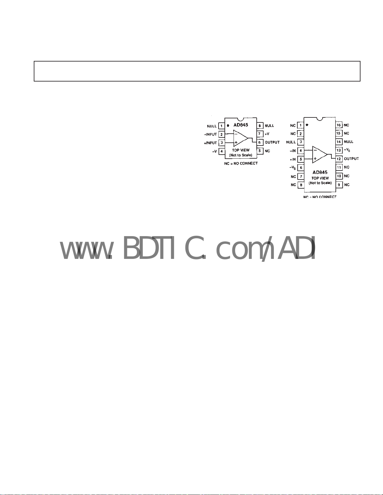
CONNECTION DIAGRAMS
Plastic Mini-DIP (N) Package
and CERDIP (Q) Package
The AD845 conforms to the standard op amp pinout except
that offset nulling is to V+. The AD845J and AD845K grade
devices are available specified to operate over the commercial
0∞C to 70∞C temperature range. AD845A and AD845B
devices are specified for operation over the –40∞C to +85∞C
industrial temperature range. The AD845S is specified to operate over the full military temperature range of –55∞C to +125∞C.
Both the industrial and military versions are available in 8-lead
CERDIP packages. The commercial version is available in an
8-lead plastic mini-DIP and 16-lead SOIC; J and S grade chips
are also available.
PRODUCT HIGHLIGHTS
1. The high slew rate, fast settling time, and dc precision of the
AD845 make it ideal for high speed applications requiring
12-bit accuracy.
2. The performance of circuits using the LF400, HA2520,
HA2522, HA2525, HA2620, HA2622, HA2625, 3550,
OPA605, and LH0062 can be upgraded in most cases.
3. The AD845 is unity gain stable and internally compensated.
4. The AD845 is specified while driving 100 pF/500 W loads.
16-Lead SOIC
(R-16) Package
REV. E
Information furnished by Analog Devices is believed to be accurate and
reliable. However, no responsibility is assumed by Analog Devices for its
use, nor for any infringements of patents or other rights of third parties that
may result from its use. No license is granted by implication or otherwise
under any patent or patent rights of Analog Devices. Trademarks and
registered trademarks are the property of their respective owners.
One Technology Way, P.O. Box 9106, Norwood, MA 02062-9106, U.S.A.
Tel: 781/329-4700 www.analog.com
Fax: 781/326-8703 © 2003 Analog Devices, Inc. All rights reserved.
AD845–SPECIFICATIONS
www.BDTIC.com/ADI
(@ 25ⴗC and ⴞ15 V dc, unless otherwise noted.)
AD845J/A AD845K/B AD845S
Parameter Conditions Min Typ Max Min Typ Max Min Typ Max Unit
INPUT OFFSET VOLTAGE
1
Initial Offset 0.7 1.5 0.1 0.25 0.25 1.0 mV
T
MIN
to T
MAX
2.5 0.4 2.0 mV
Offset Drift 20 1.5 5.0 10 mV/∞C
INPUT BIAS CURRENT
2
Initial VCM = 0 V 0.75 2 0.5 1 0.75 2 nA
T
MIN
to T
MAX
45/75 18/38 500 nA
INPUT OFFSET CURRENT
Initial VCM = 0 V 25 300 15 100 25 300 pA
T
to T
MIN
MAX
INPUT CHARACTERISTICS
Input Resistance 10
11
3/6.5 1.2/2.6 20 nA
10
11
10
11
kW
Input Capacitance 4.0 4.0 4.0 pF
INPUT VOLTAGE RANGE
Differential ±20 ±20 ± 20 V
Common-Mode ⴞ10 +10.5/–13 ⴞ10 +10.5/–13 ⴞ10 +10.5/–13 V
Common-Mode Rejection VCM = ±10 V 86 110 94 113 86 110 dB
INPUT VOLTAGE NOISE 0.1 Hz to 10 Hz 4 4 4 mV p-p
f = 10 Hz 80 80 80 nV/÷Hz
f = 100 Hz 60 60 60 nV/÷Hz
f = 1 kHz 25 25 25 nV/÷Hz
f = 10 kHz 18 18 18 nV/÷Hz
f = 100 kHz 12 12 12 nV/÷Hz
INPUT CURRENT NOISE f = 1 kHz 0.1 0.1 0.1 pA/÷Hz
OPEN-LOOP GAIN V
= ±10 V
O
R
≥ 2 kW 200 500 250 500 200 500 V/mV
LOAD
R
≥ 500 W 100 250 125 250 100 250 V/mV
LOAD
T
MIN–TMAX
70 75 50 V/mV
OUTPUT CHARACTERISTICS
Voltage R
≥ 500 W ⴞ12.5 ⴞ12.5 ⴞ12.5 V
LOAD
Current Short Circuit 50 50 50 mA
Output Resistance Open Loop 5 5 5 W
FREQUENCY RESPONSE
Small Signal Unity Gain 12.8 16 13.6 16 13.6 16 MHz
Full Power Bandwidth
3
VO = ±10 V
R
= 500 W 1.75 1.75 1.75 MHz
LOAD
Rise Time 20 20 20 ns
Overshoot 20 20 20 %
Slew Rate 80 100 94 100 94 100 V/ms
Settling Time 10 V Step
C
= 100 pF
LOAD
R
= 500 W
LOAD
to 0.01% 350 350 500 350 500 ns
to 0.1% 250 250 250 ns
DIFFERENTIAL GAIN f = 4.4 MHz 0.04 0.04 0.04 %
DIFFERENTIAL PHASE f = 4.4 MHz 0.02 0.02 0.02 Degree
POWER SUPPLY
Rated Performance ±15 ±15 ± 15 V
Operating Range ⴞ4.75 ⴞ18 ⴞ4.75 ⴞ18 ⴞ4.75 ⴞ18 V
Rejection Ratio V
Quiescent Current T
NOTES
1
Input offset voltage specifications are guaranteed after five minutes of operation at TA = 25∞C.
2
Bias current specifications are guaranteed maximum at either input after five minutes of operation at T
3
FPBW = slew rate/2 p V peak.
4
S grade T
All min and max specifications are guaranteed. Specifications shown in boldface are tested on all production units at final electrical test. Results from these tests are
used to calculate outgoing quality levels.
Specifications subject to change without notice.
MIN–TMAX
are tested with automatic test equipment at TA = –55∞C and TA = +125∞C.
= ± 5 to ±15 V 88 110 95 113 88 110 dB
S
MIN
to T
MAX
10 12 10 12 10 12 mA
= 25∞C.
A
–2–
REV. E
AD845
www.BDTIC.com/ADI
ABSOLUTE MAXIMUM RATINGS
Supply Voltage . . . . . . . . . . . . . . . . . . . . . . . . . . . . . . . . ± 18 V
Internal Power Dissipation
2
1
Plastic Mini-DIP . . . . . . . . . . . . . . . . . . . . . . . . . . . . .1.6 W
CERDIP . . . . . . . . . . . . . . . . . . . . . . . . . . . . . . . . . . .1.4 W
16-Lead SOIC . . . . . . . . . . . . . . . . . . . . . . . . . . . . . . . 1.5 W
Input Voltage . . . . . . . . . . . . . . . . . . . . . . . . . . . . . . . . . . . +V
S
Output Short-Circuit Duration . . . . . . . . . . . . . . . . Indefinite
Differential Input Voltage . . . . . . . . . . . . . . . . . . +V
and –V
S
S
Storage Temperature Range
Q . . . . . . . . . . . . . . . . . . . . . . . . . . . . . . . .–65∞C to +150∞C
N, R . . . . . . . . . . . . . . . . . . . . . . . . . . . . . .–65∞C to +125∞C
Lead Temperature Range (Soldering 60 sec) . . . . . . . . . 300∞C
NOTES
1
Stresses above those listed under Absolute Maximum Ratings may cause permanent damage to the device. This is a stress rating only, and functional operation of
the device at these or any other conditions above those indicated in the operational
sections of this specification is not implied. Exposure to absolute maximum rating
conditions for extended periods may affect device reliability.
2
Mini-DIP package: qJA = 100∞C/W; CERDIP package: qJA = 110∞C/W; SOIC
package: qJA = 100∞C/W.
ORDERING GUIDE
Temperature Package Package
Model Range Description Option
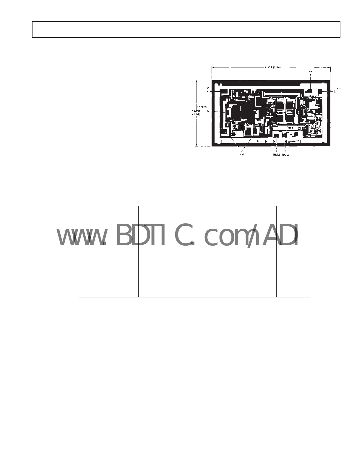
METALIZATION PHOTOGRAPH
Dimensions shown in inches and (mm).
Contact factory for latest dimensions.
SUBSTRATE CONNECTED TO +V
S
1
AD845JN 0∞C to 70∞C 8-Lead PDIP N-8
AD845KN 0∞C to 70∞C 8-Lead PDIP N-8
AD845JR-16 0∞C to 70∞C 16-Lead SOIC R-16
AD845JR-16-REEL 0∞C to 70∞CTape and Reel R-16
AD845JR-16-REEL7 0∞C to 70∞CTape and Reel R-16
AD845AQ –40∞C to +85∞C 8-Lead CERDIP Q-8
AD845BQ –40∞C to +85∞C 8-Lead CERDIP Q-8
AD845SQ –55∞C to +125∞C 8-Lead CERDIP Q-8
AD845SQ/883B –55∞C to +125∞C 8-Lead CERDIP Q-8
5962-8964501PA
2
–55∞C to +125∞C 8-Lead CERDIP Q-8
AD845JCHIPS 0∞C to 70∞CDie
NOTES
1
N = Plastic DIP; Q = CERDIP; R = Small Outline IC (SOIC).
2
See military data sheet.
REV. E
–3–
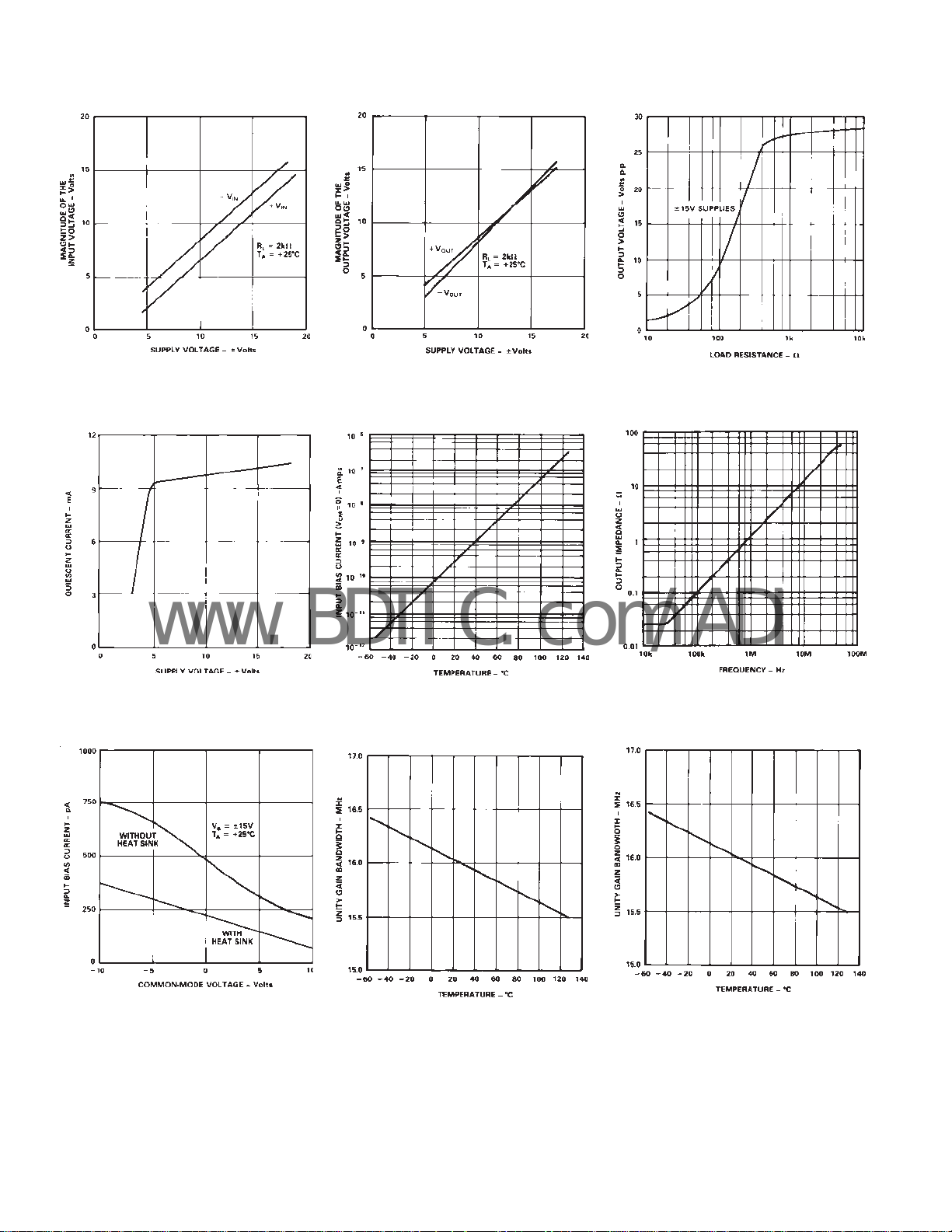
AD845–Typical Performance Characteristics
www.BDTIC.com/ADI
TPC 1. Input Voltage Swing
vs. Supply Voltage
TPC 4. Quiescent Current vs.
Supply Voltage
TPC 2. Output Voltage Swing
vs. Supply Voltage
TPC 5. Input Bias Current vs.
Temperature
TPC 3. Output Voltage Swing
vs. Resistive Load
TPC 6. Magnitude of Output
Impedance vs. Frequency
TPC 7. Input Bias Current vs.
Common-Mode Voltage
TPC 8. Short-Circuit Current
Limit vs. Temperature
–4–
TPC 9. Unity-Gain Bandwidth
vs. Temperature
REV. E

AD845
www.BDTIC.com/ADI
TPC 10. Open-Loop Gain and
Phase Margin vs. Frequency
TPC 13. Common-Mode
Rejection vs. Frequency
TPC 11. Open-Loop Gain vs.
Supply Voltage
TPC 14. Large Signal Frequency
Response
TPC 12. Power Supply
Rejection vs. Frequency
TPC 15. Output Swing and
Error vs. Settling Time
TPC 16. Harmonic Distortion
vs. Frequency
REV. E
TPC 17. Input Noise Voltage
Spectral Density
–5–
TPC 18. Slew Rate vs. Temperature

AD845
www.BDTIC.com/ADI
TPC 19. Recommended Power
Supply Bypassing
TPC 22. Unity Gain Follower
TPC 20. AD845 Simplified
Schematic
TPC 23. Unity Gain Follower
Large Signal Pulse Response
TPC 21. Offset Null Configuration
TPC 24. Unity Gain Follower
Small Signal Pulse Response
TPC 25. Unity Gain Inverter
TPC 26. Unity Gain Inverter
Large Signal Pulse Response
–6–
TPC 27. Unity Gain Inverter
Small Signal Pulse Response
REV. E

AD845
www.BDTIC.com/ADI
MEASURING AD845 SETTLING TIME
Figure 1 shows AD845 settling time performance. This measurement was accomplished by driving the amplifier in the unity
gain inverting mode with a fast pulse generator. The input
summing junction was measured using false nulling techniques.
Settling time is defined as the interval of time from the application
of an ideal step function input until the closed-loop amplifier
output has entered and remains within a specified error band.
Components of settling time include:
1. Propagation time through the amplifier
2. Slewing time to approach the final output value
3. Recovery time from overload associated with the slewing
4. Linear settling to within a specified error band
These individual components can be seen easily in Figure 1.
Settling time is extremely important in high speed applications
where the current output of a DAC must be converted to a
voltage. When driving a 500 W load in parallel with a 100 pF
capacitor, the AD845 settles to 0.1% in 250 ns and to 0.01% in
310 ns.
stable, accurately defined gain. Low input bias currents and fast
settling are achieved with the FET input AD845.
Most monolithic instrumentation amplifiers do not have the
high frequency performance of the circuit in Figure 3. The circuit bandwidth is 10.9 MHz at a gain of 1 and 8.8 MHz at a
gain of 10; settling time for the entire circuit is 900 ns to 0.01%
for a 10 V step (Gain = 10).
The capacitors employed in this circuit greatly improve the
amplifier’s settling time and phase margin.
Figure 1. Settling Characteristics 0 V to 10 V Step
Upper Trace: Output of AD845 Under Test (5 V/Div)
Lower Trace: Error Voltage (1 mV/Div)
Figure 2. Settling Time Test Circuit
Figure 3. High Performance, High Speed Instrumentation
Amplifier
Table I. Performance Summary for the 3-Op Amp
Instrumentation Amplifier Circuit
3-Op Amp In-Amp
Small Signal Settling Time
Gain R
1Open 10.9 MHz 500 ns
22 kW 8.8 MHz 500 ns
10 226 W 2.6 MHz 900 ns
100 20 W 290 kHz 7.5 ms
Note: Resistors around the amplifiers’ input pins need to be small enough in
value so that the RC time constant they form, with stray circuit capacitance,
does not reduce circuit bandwidth.
G
Bandwidth to 0.01%
A HIGH SPEED INSTRUMENTATION AMP
The 3-op amp instrumentation amplifier circuit shown in
Figure 3 can provide a range of gains from unity up to 1000 and
higher. The instrumentation amplifier configuration features
high common-mode rejection, balanced differential inputs, and
REV. E
Figure 4. The Pulse Response of the 3-Op Amp
Instrumentation Amplifier. Gain = 1, Horizontal Scale =
0.5 ms/Div and Vertical Scale = 5 V/Div.
–7–

AD845
www.BDTIC.com/ADI
Figure 5. Settling Time of the 3-Op Amp Instrumentation
Amplifier. Horizontal Scale is 200 ns/Div, Vertical Scale,
Positive Pulse Input is 5 V/Div and Output Settling is
1 mV/Div.
DRIVING THE ANALOG INPUT OF AN A/D CONVERTER
An op amp driving the analog input of an A/D converter, such
as that shown in Figure 7, must be capable of maintaining a
constant output voltage under dynamically changing load conditions. In successive approximation converters, the input current
is compared to a series of switched trial currents. The comparison point is diode clamped but may deviate several hundred
millivolts, resulting in high frequency modulation of A/D input
current. The output impedance of a feedback amplifier is made
artificially low by the loop gain. At high frequencies, where the
loop gain is low, the amplifier output impedance can approach
its open-loop value. Most IC amplifiers exhibit a minimum
open-loop output impedance of 25 W due to current limiting
resistors. A few hundred microamps reflected from the change
in converter loading can introduce errors in instantaneous input
voltage. If the A/D conversion speed is not excessive and the
bandwidth of the amplifier is sufficient, the amplifier’s output
will return to the nominal value before the converter makes its
comparison. However, many amplifiers have relatively narrow
bandwidth, yielding slow recovery from output transients. The
Figure 6. Settling Time of the Three Op Amp Instrumentation Amplifier. Horizontal Scale: 200 ns/Div; Vertical
Scale, Negative Pulse Input: 5 V/ Div; Output Settling:
1 mV/Div.
AD845 is ideally suited to drive high resolution A/D converters
with 5 ms or longer conversion times since it offers both wide
bandwidth and high open-loop gain.
Figure 7. AD845 As ADC Unity Gain Buffer
–8–
REV. E

OUTLINE DIMENSIONS
www.BDTIC.com/ADI
AD845
8-Lead Plastic Dual In-Line Package [PDIP]
(N-8)
Dimensions shown in inches and (millimeters)
0.375 (9.53)
0.365 (9.27)
0.355 (9.02)
8
1
0.100 (2.54)
0.180
(4.57)
MAX
0.150 (3.81)
0.130 (3.30)
0.110 (2.79)
0.022 (0.56)
0.018 (0.46)
0.014 (0.36)
CONTROLLING DIMENSIONS ARE IN INCHES; MILLIMETER DIMENSIONS
(IN PARENTHESES) ARE ROUNDED-OFF INCH EQUIVALENTS FOR
REFERENCE ONLY AND ARE NOT APPROPRIATE FOR USE IN DESIGN
COMPLIANT TO JEDEC STANDARDS MO-095AA
BSC
5
4
0.295 (7.49)
0.285 (7.24)
0.275 (6.98)
0.015
(0.38)
MIN
SEATING
PLANE
0.060 (1.52)
0.050 (1.27)
0.045 (1.14)
0.325 (8.26)
0.310 (7.87)
0.300 (7.62)
0.150 (3.81)
0.135 (3.43)
0.120 (3.05)
0.015 (0.38)
0.010 (0.25)
0.008 (0.20)
16-Lead Standard Small Outline Package [SOIC]
Wide Body
(R-16)
Dimensions shown in millimeters and (inches)
10.50 (0.4134)
10.10 (0.3976)
16
1
1.27 (0.0500)
BSC
0.30 (0.0118)
0.10 (0.0039)
COPLANARITY
0.10
CONTROLLING DIMENSIONS ARE IN MILLIMETERS; INCH DIMENSIONS
(IN PARENTHESES) ARE ROUNDED-OFF MILLIMETER EQUIVALENTS FOR
REFERENCE ONLY AND ARE NOT APPROPRIATE FOR USE IN DESIGN
0.51 (0.0201)
0.31 (0.0122)
COMPLIANT TO JEDEC STANDARDS MS-013AA
9
7.60 (0.2992)
7.40 (0.2913)
8
2.65 (0.1043)
2.35 (0.0925)
SEATING
PLANE
10.65 (0.4193)
10.00 (0.3937)
0.33 (0.0130)
0.20 (0.0079)
8ⴗ
0ⴗ
0.75 (0.0295)
0.25 (0.0098)
1.27 (0.0500)
0.40 (0.0157)
ⴛ 45ⴗ
8-Lead Ceramic Dual In-Line Package [CERDIP]
(Q-8)
Dimensions shown in inches and (millimeters)
0.005 (0.13)
PIN 1
0.200 (5.08)
MAX
0.200 (5.08)
0.125 (3.18)
0.023 (0.58)
0.014 (0.36)
CONTROLLING DIMENSIONS ARE IN INCHES; MILLIMETERS DIMENSIONS
(IN PARENTHESES) ARE ROUNDED-OFF INCH EQUIVALENTS FOR
REFERENCE ONLY AND ARE NOT APPROPRIATE FOR USE IN DESIGN
0.055 (1.40)
MIN
0.100 (2.54) BSC
0.405 (10.29) MAX
MAX
85
1
4
0.070 (1.78)
0.030 (0.76)
0.310 (7.87)
0.220 (5.59)
0.060 (1.52)
0.015 (0.38)
0.150 (3.81)
MIN
SEATING
PLANE
0.320 (8.13)
0.290 (7.37)
15
0
0.015 (0.38)
0.008 (0.20)
REV. E
–9–

AD845
www.BDTIC.com/ADI
Revision History
Location Page
10/03—Data Sheet changed from REV. D to REV. E.
Renumbered figures and TPCs . . . . . . . . . . . . . . . . . . . . . . . . . . . . . . . . . . . . . . . . . . . . . . . . . . . . . . . . . . . . . . . . . . . . . . . Universal
Updated OUTLINE DIMENSIONS . . . . . . . . . . . . . . . . . . . . . . . . . . . . . . . . . . . . . . . . . . . . . . . . . . . . . . . . . . . . . . . . . . . . . . . . 9
–10–
REV. E

–11–
www.BDTIC.com/ADI

C00886–0–10/03(E)
www.BDTIC.com/ADI
–12–
 Loading...