

Page 1
xDSL Line Driver
a
FEATURES
Ideal xDSL Line Driver for VoDSL or Low Power
Applications such as USB, PCMCIA, or PCI Based
Customer Premise Equipment (CPE)
High Output Voltage and Current Drive
340 mA Output Drive Current
Low Power Operation
3 V to 12 V Power Supply Range
1-Pin Logic Controlled Standby, Shutdown
Low Supply Current of 19 mA (Typical)
Low Distortion
–82 dBc SFDR, 12 V p-p into Differential 21 @ 100 kHz
4.5 nV/√Hz Input Voltage Noise Density, 100 kHz
Out-of-Band SFDR = –72 dBc, 144 kHz to 500 kHz,
= 100 , P
Z
LINE
High Speed
40 MHz Bandwidth (–3 dB)
375 V/s Slew Rate
APPLICATIONS
VoDSL Modems
xDSL USB, PCI, PCMCIA Cards
Line Powered or Battery Backup xDSL Modems
= 13.5 dBm
LINE
3V to 12 V with Power-Down
AD8391
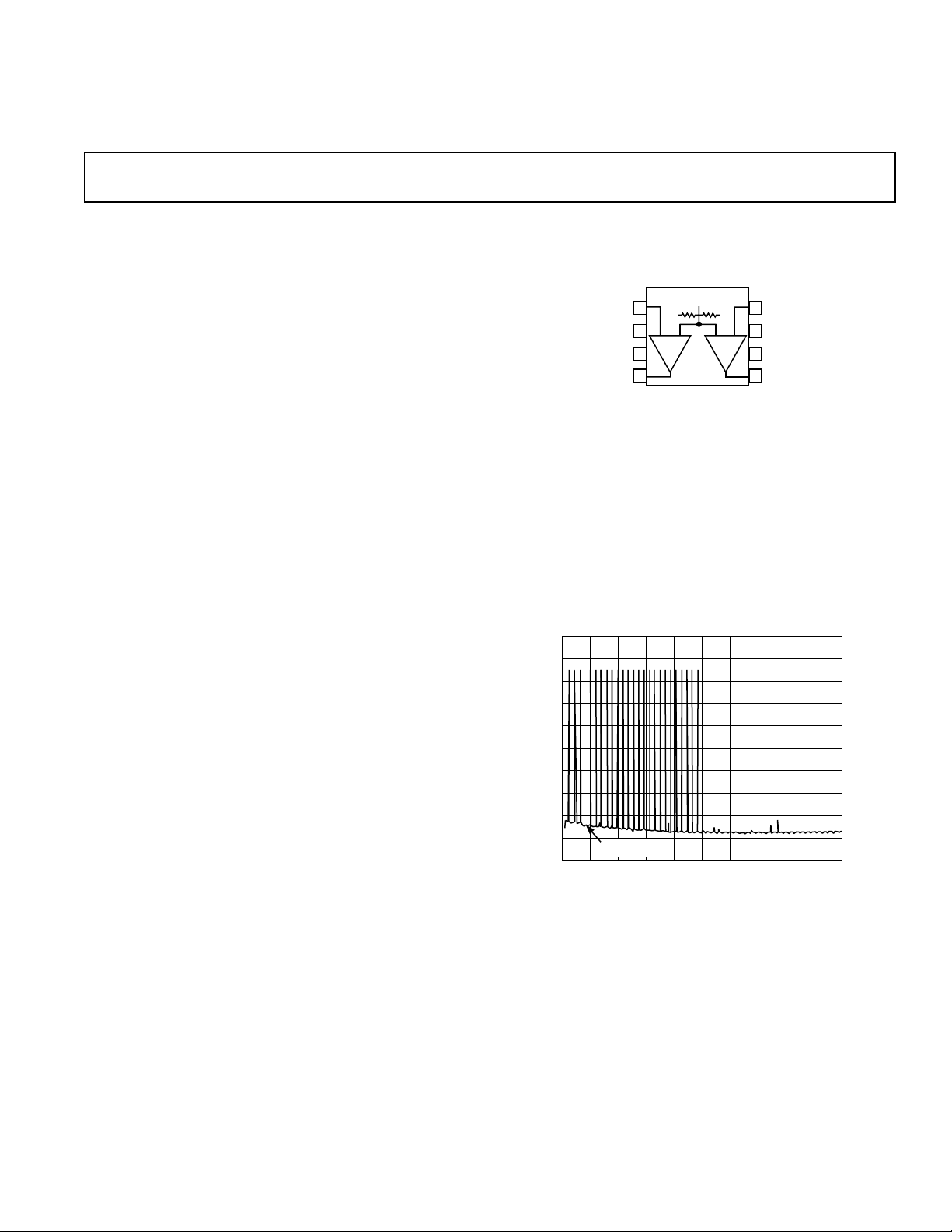
PIN CONFIGURATION
8-Lead SOIC
(Thermal Coastline)
V
MID
IN1
PWDN
+V
V
OUT
V
1
2
3
S
4
1
S
AD8391
V
8
IN2
S
V
7
MID
6
–V
S
5
V
2
OUT
PRODUCT DESCRIPTION
The AD8391 consists of two parallel, low cost xDSL line drive
amplifiers capable of driving low distortion signals while running on
both 3 V to 12 V single-supply or equivalent dual-supply rails. It is
primarily intended for use in single-supply xDSL systems where low
power is essential, such as line powered and battery backup systems.
Each amplifier output drives more than 250 mA of current while
maintaining –82 dBc of SFDR at 100 kHz on 12 V, outstanding
performance for any xDSL CPE application.
The AD8391 provides a flexible power-down feature consisting of
a 1-pin digital control line. This allows biasing of the AD8391 to
full power (Logic 1), standby (Logic three-state maintains low
amplifier output impedance), and shutdown (Logic 0 places
amplifier outputs in a high impedance state). PWDN is referenced to –V
.
S
Fabricated on ADI’s high speed XFCB process, the high bandwidth
and fast slew rate of the AD8391 keep distortion to a minimum,
while dissipating a minimum of power. The quiescent current of the
AD8391 is low: 19 mA total static current draw. The AD8391
comes in a compact 8-lead SOIC “thermal coastline” package and
operates over the temperature range –40°C to +85°C.
REV. A
UPSTREAM POWER – 10dB/DIV
EMPTY BIN
25 250137.5
FREQUENCY – kHz
Figure 1. Upstream Transit Spectrum with Empty Bin
at 45 kHz; Line Power = 12.5 dBm into 100
Ω
Information furnished by Analog Devices is believed to be accurate and
reliable. However, no responsibility is assumed by Analog Devices for its
use, nor for any infringements of patents or other rights of third parties that
may result from its use. No license is granted by implication or otherwise
under any patent or patent rights of Analog Devices. Trademarks and
registered trademarks are the property of their respective owners.
One Technology Way, P.O. Box 9106, Norwood, MA 02062-9106, U.S.A.
Tel: 781/329-4700 www.analog.com
Fax: 781/326-8703 © 2003 Analog Devices, Inc. All rights reserved.
Page 2

AD8391–SPECIFICATIONS
(@ 25C, VS= 12 V, RL = 10 , V
unless otherwise noted. See TPC 1 for Basic Circuit Configuration.)
= VS/2, G = –2, RF= 909 , RG= 453 ,
MID
Parameter Conditions Min Typ Max Unit
DYNAMIC PERFORMANCE
–3 dB Bandwidth G = –1, V
G = –2, V
0.1 dB Bandwidth V
Large Signal Bandwidth V
Slew Rate V
Rise and Fall Time V
< 0.4 V p-p 4 MHz
OUT
= 4 V p-p 50 MHz
OUT
= 4 V p-p 375 V/µs
OUT
= 4 V p-p 8 ns
OUT
Settling Time 0.1%, V
< 0.4 V p-p, RG = 909 Ω 40 MHz
OUT
< 0.4 V p-p 38 MHz
OUT
= 2 V p-p 60 ns
OUT
NOISE/HARMONIC
PERFORMANCE
Distortion, G = –5 (RG = 178 Ω)V
Second Harmonic 100 kHz, R
= 8 V p-p (Differential)
OUT
= 21 Ω –82 dBc
L
Third Harmonic 100 kHz, RL = 21 Ω –95 dBc
MTPR (In-Band) 25 kHz to 138 kHz, R
SFDR (Out-of-Band) 144 kHz to 500 kHz, R
= 21 Ω –70 dBc
L
= 21 Ω –72 dBc
L
Input Noise Voltage f = 100 kHz Differential 4.5 nV/√Hz
Input Noise Current f = 100 kHz 9 pA/√Hz
Crosstalk f = 1 MHz, G = –2, Output to Output 64 dB
DC PERFORMANCE
Input Offset Voltage V
= +VS/2 ±2 ±15 mV
MID
to T
T
V
MIN
MID
MAX
= Float ±2mV
±3mV
Input Offset Voltage Match ±0.25 ±2.6 mV
T
Transimpedance ∆V
to T
MIN
MAX
= 5 V 10 MΩ
OUT
±0.35 mV
INPUT CHARACTERISTICS
Input Resistance 125 Ω
Input Bias Current In1, In2 pins 2.5 10 µA
Input Bias Current Match In1 – In2 ±0.5 ±6 µA
CMRR V
= VIN = 5.5 V to 6.5 V, ∆V
MID
/∆VIN, cm 48 dB
OS
Input CM Voltage Range 1.2 to 10.8 V
Accuracy V
V
MID
Input Resistance 2.5 kΩ
V
MID
V
Input Capacitance 10 pF
MID
= Float Delta from +VS/2 ±5 ±30 mV
MID
OUTPUT CHARACTERISTICS
Output Resistance Frequency = 100 kHz, PWDN 1 0.3 Ω
Output Resistance Frequency = 100 kHz, PWDN 0 3 kΩ
Output Voltage Swing R
Linear Output Current SFDR < –75 dBc, f = 100 kHz, R
= 100 Ω 0.1 11.9 V
LOAD
= 21 Ω 340 mA
L
Short-Circuit Current 1500 mA
POWER SUPPLY
Supply Current PWDN = 1 16 19 21 mA
T
MIN
to T
MAX
22 mA
STBY Supply Current PWDN = Open or Three-State 10 mA
SHUTDOWN Supply Current PWDN = 0 4 6 mA
Operating Range Single Supply 3.0 12 V
Power Supply Rejection Ratio V
= VS /2, ∆VS = ± 0.5 V 55 dB
MID
LOGIC INPUT (PWDN)
Logic 1 Voltage –VS + 2.0 V
Logic 0 Voltage –V
+ 0.8 V
S
Logic Input Bias Current ± 300 µA
Turn-On Time RL = 21 Ω, IS = 90% of Typical 200 ns
Specifications subject to change without notice.
–2–
REV. A
Page 3

AD8391
SPECIFICATIONS
(@ 25C, VS=3 V, RL = 10 , V
See TPC 1 for Basic Circuit Configuration.)
= VS/2, G = –2, RF= 909 , RG= 453 , unless otherwise noted.
MID
Parameter Conditions Min Typ Max Unit
DYNAMIC PERFORMANCE
–3 dB Bandwidth G = –1, V
G = –2, V
0.1 dB Bandwidth V
Large Signal Bandwidth V
Slew Rate V
< 0.4 V p-p 3.5 MHz
OUT
= 2 V p-p 30 MHz
OUT
=2V p-p 50 V/µs
OUT
Rise and Fall Time Differential, V
Settling Time 0.1%, V
< 0.4 V p-p 37 MHz
OUT
< 0.4 V p-p 36 MHz
OUT
= 1 V p-p 15 ns
OUT
= 2 V p-p 110 ns
OUT
NOISE/HARMONIC
PERFORMANCE
Distortion V
= 4 V p-p (Differential)
OUT
Second Harmonic 100 kHz, RL= 21 Ω –81 dBc
Third Harmonic 100 kHz, R
= 21 Ω –97 dBc
L
Input Noise Voltage f = 100 kHz Differential 4.5 nV/√Hz
Input Noise Current f = 100 kHz 9 pA/√Hz
DC PERFORMANCE
Input Offset Voltage V
= +VS/2 ±3 ±15 mV
MID
to T
T
V
MIN
MID
MAX
= Float ±3mV
±4mV
Input Offset Voltage Match ± 0.1 ±2.6 mV
T
Transimpedance ∆V
to T
MIN
MAX
= 1 V 8 MΩ
OUT
±0.2 mV
INPUT CHARACTERISTICS
Input Resistance 125 Ω
Input Bias Current In1, In2 pins 1 7 µA
Input Bias Current Match In1 – In2 ±0.5 ±4 µA
CMRR V
VIN= 1.3 V to 1.5 V, ∆VOS /∆VIN, cm
MID
48 dB
=
Input CM Voltage Range 1.2 to 2.1 V
Accuracy V
V
MID
Input Resistance 2.5 kΩ
V
MID
V
Input Capacitance 10 pF
MID
= Float, Delta from +VS/2 ±5 ±30 mV
MID
OUTPUT CHARACTERISTICS
Output Resistance Frequency = 100 kHz, PWDN 1 0.2 Ω
Output Resistance Frequency = 100 kHz, PWDN 0 9 kΩ
Output Voltage Swing R
Linear Output Current SFDR < –82 dBc, f = 100 kHz, R
= 100 Ω 0.1 2.9 V
L
= 21 Ω 125 mA
L
Short-Circuit Current 1000 mA
POWER SUPPLY
Supply Current PWDN = 1 13 16 18 mA
T
MIN
to T
MAX
19 mA
STBY Supply Current PWDN = Open or Three-State 8 mA
SHUTDOWN Supply Current PWDN = 0 1 2 mA
Operating Range Single Supply 3.0 12 V
Power Supply Rejection Ratio V
= VS/2, ∆VS = ±0.5 V 55 dB
MID
LOGIC INPUTS (PWDN [1,0])
Logic 1 Voltage –VS + 2.0 V
Logic 0 Voltage –V
+ 0.8 V
S
Logic Input Bias Current ± 60 µA
Turn-On Time RL = 21 Ω, IS = 90% of Typical 200 ns
Specifications subject to change without notice.
REV. A
–3–
Page 4
AD8391
ABSOLUTE MAXIMUM RATINGS
Supply Voltage . . . . . . . . . . . . . . . . . . . . . . . . . . . . . . . . 12.6 V
Internal Power Dissipation
2
1
Small Outline Package (R) . . . . . . . . . . . . . . . . . . . 650 mW
Input Voltage (Common-Mode) . . . . . . . . . . . . . . . . . . . . ± V
Logic Voltage, PWDN . . . . . . . . . . . . . . . . . . . . . . . . . . . . ±V
S
S
Output Short-Circuit Duration
. . . . . . . . . . . . . . . . . . . . .Observe Power Derating Curve
Storage Temperature Range . . . . . . . . . . . . –65°C to +150°C
Operating Temperature Range . . . . . . . . . . . –40°C to +85°C
Lead Temperature Range (Soldering 10 sec) . . . . . . . . . 300°C
NOTES
1
Stresses above those listed under Absolute Maximum Ratings may cause permanent damage to the device. This is a stress rating only; functional operation of the
device at these or any other conditions above those indicated in the operational
section of this specification is not implied. Exposure to absolute maximum rating
conditions for extended periods may affect device reliability.
2
Specification is for device on a 4-layer board in free air at 85°C: 8-Lead SOIC
package: JA = 100°C/W.
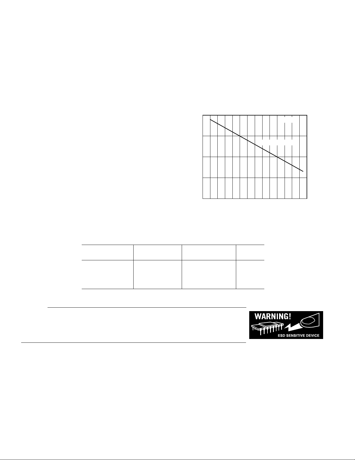
MAXIMUM POWER DISSIPATION
The maximum power that can be safely dissipated by the
AD8391 is limited by the associated rise in junction temperature.
The maximum safe junction temperature for a plastic encapsulated device is determined by the glass transition temperature of
the plastic, approximately 150°C. Temporarily exceeding this
limit may cause a shift in parametric performance due to a change
in the stresses exerted on the die by the package.
To ensure proper operation, it is necessary to observe the maximum power derating curve.
2.0
1.5
8-LEAD SOIC PACKAGE
1.0
0.5
MAXIMUM POWER DISSIPATION – W
0
–50
–40 –30 –20 –10 0 10 20 30 40 50 60 70 80 90
AMBIENT TEMPERATURE – C
TJ = 150C
Figure 2. Plot of Maximum Power Dissipation
vs. Temperature
ORDERING GUIDE
Temperature Package Package
Model Range Description Option
AD8391AR –40°C to +85°C 8-Lead SOIC R-8
AD8391AR–REEL –40°C to +85°C 8-Lead SOIC R-8
AD8391AR–REEL7 –40°C to +85°C 8-Lead SOIC R-8
AD8391AR–EVAL Evaluation Board
CAUTION
ESD (electrostatic discharge) sensitive device. Electrostatic charges as high as 4000 V readily
accumulate on the human body and test equipment and can discharge without detection. Although
the AD8391 features proprietary ESD protection circuitry, permanent damage may occur on
devices subjected to high energy electrostatic discharges. Therefore, proper ESD precautions are
recommended to avoid performance degradation or loss of functionality.
–4–
REV. A
Page 5
Typical Performance Characteristics–AD8391
TIME – ns
0.3
OUTPUT VOLTAGE – V
0.2
0.1
0
–0.1
–0.2
–0.4
1007550250 125 150 175 200 225 250
–0.3
0.4
VS = 1.5V
G
= –2
R
L
= 10
CF = 3pF
CF = 0pF
TIME – ns
1.5
OUTPUT VOLTAGE – V
1.0
0.5
0
–0.5
–1.0
–2.0
1007550250 125 150 175 200 225 250
–1.5
2.0
VS = 1.5V
G
= –2
R
L
= 10
CF = 3pF
CF = 0pF
TIME – ns
0.01
0 30050
OUTPUT ERROR – V
100 150 200 250
0.008
0.006
0.004
0.002
0
–0.002
–0.004
–0.006
–0.008
–0.01
VS = 6V
G
= –2
V
IN
= 1V p-p
OUTPUT ERROR
C
F
R
G
V
IN
~
V
MID
0.1F
TPC 1. Single-Ended Test Circuit
0.4
0.3
0.2
0.1
0
–0.1
OUTPUT VOLTAGE – V
–0.2
CF = 0pF
CF = 3pF
R
F
R
L
+
0.1F
+
0.1F
6.8F
6.8F
V
OUT
+V
S
–V
TPC 4. Small Signal Step Response
VS = 6V
G
= –2
R
= 10
L
REV. A
–0.3
–0.4
1007550250
125 150 175 200 225 250
TIME – ns
TPC 2. Small Signal Step Response
4
3
2
1
0
–1
OUTPUT VOLTAGE – V
–2
–3
–4
TPC 3. Large Signal Step Response
CF = 0pF
C
= 3pF
F
1007550250 125 150 175 200 225 250
TIME – ns
VS = 6V
G
= –2
R
= 10
L
TPC 5. Large Signal Step Response
TPC 6. 0.1% Settling Time
–5–
Page 6
AD8391
12
9
6
3
0
–3
–6
–9
OUTPUT VOLTAGE – dBV
–12
–15
–18
0.1 1 100010 100
FREQUENCY – MHz
TPC 7. Output Voltage vs. Frequency
1500
VS = 6V
1250
1000
750
VOH @+85C
V
@+25C
OH
@–40C
V
OH
VS = 6V
= 10
R
L
= –2
G
6
3
0
–3
–6
–9
–12
–15
OUTPUT VOLTAGE – dBV
–18
–21
–24
0.1 1 100010 100
FREQUENCY – MHz
TPC 10. Output Voltage vs. Frequency
1200
VS = 1.5V
1000
800
600
@
V
+85C
OH
@
+25C
V
OH
@
–40C
V
OH
V
OL@
VS = 1.5V
= 10
R
L
G
= –2
–40C
500
V
@+85C
OL
@+25C
V
250
OUTPUT SATURATION VOLTAGE – m V
0
LOAD CURRENT – mA
OL
V
OL
TPC 8. Output Saturation Voltage vs. Load
18
15
12
9
6
3
GAIN – dB
0
–3
–6
–9
0.1 1 100010 100
STANDBY
FULL POWER
FREQUENCY – MHz
TPC 9. Small Signal Frequency Response
@–40C
900800600 7005004003002001000
= 6V
V
S
R
= 10
L
= 2
G
1000
400
200
OUTPUT SATURATION VOLTAGE – m V
0
LOAD CURRENT – mA
V
V
OL@
OL
@
+25C
+85C
450400300 350250200150100500
TPC 11. Output Saturation Voltage vs. Load
18
15
12
9
6
3
GAIN – dB
0
–3
–6
–9
0.1 1 100010 100
STANDBY
FREQUENCY – MHz
VS = 1.5V
R
= 10
L
= 2
G
FULL POWER
TPC 12. Small Signal Frequency Response
500
–6–
REV. A
Page 7

AD8391
FREQUENCY – MHz
0.1 1 100010 100
SIGNAL FEEDTHROUGH – dB
–15
–20
–25
–30
–35
–40
–45
–50
V
S
= 6V
R
L
= 10
POWER-DOWN
V
IN
= 10dBm
–55
G = –5, RG = 178, RF = 909
G
= –2, RG = 453, RF = 909
60
50
VS = 6V
100 1k 10k 100k
FREQUENCY – Hz
VOLTA G E NOISE – nV/ Hz
40
30
20
VS = 1.5V
10
0
TPC 13. Voltage Noise vs. Frequency (RTI)
10k
VS = 6V
1k
100
POWER-DOWN
140
120
= 1.5V
V
100
80
60
40
CURRENT NOISE – pA/ Hz
VS = 6V
20
1M10
0
10 1M
S
100 1k 10k 100k
FREQUENCY – Hz
TPC 16. Current Noise vs. Frequency (RTI)
10k
VS = 1.5V
1k
100
POWER-DOWN
10
OUTPUT IMPEDANCE –
1
0.1
0.01 10000.1
POWER-UP
110100
FREQUENCY – MHz
TPC 14. Output Impedance vs. Frequency
20
0
–20
–40
–60
CROSSTALK – dB
–80
–100
–120
0.1 1 100010 100
POWER-UP
FREQUENCY – MHz
POWER-DOWN
TPC 15. Crosstalk (Output to Output)
vs. Frequency
VIN = 10dBm
= 6V
V
S
= 10
R
L
= –2
G
10
OUTPUT IMPEDANCE –
1
0.1
0.01 10000.1
POWER-UP
110100
FREQUENCY – MHz
TPC 17. Output Impedance vs. Frequency
TPC 18. Signal Feedthrough vs. Frequency
REV. A
–7–
Page 8

AD8391
R
G
V
IN+
V
MID
C
MID
R
G
V
IN–
R
F
V
OUT–
R
L
V
OUT+
R
F
TPC 19. Differential Output Test Setup
–30
V
= 6V
S
–40
RL = 21
G
= –5, (RG = 178)
–50
–60
–70
–80
–90
DIFFERENTIAL DISTORTION – dBc
–100
–110
2226
HD2 (FO = 500kHz)
HD3 (FO = 500kHz)
HD2 (FO = 100kHz)
HD3 (FO = 100kHz)
10 14 18
OUTPUT VOLTAGE – V p-p
TPC 20. Differential Distortion vs. Output Voltage
–30
RL = 21
FOR VS = 6V, V
–40
FOR V
S
G = –5
–50
–60
–70
HD2@VS = 6V
–80
–90
DIFFERENTIAL DISTORTION – dBc
–100
–110
0.01 100.1
= 1.5V, V
HD2 @VS = 1.5V
= 8V p-p
OUT
= 2V p-p
OUT
HD3 @V
FREQUENCY – MHz
HD3 @V
= 6V
S
1
= 1.5V
S
TPC 22. Differential Distortion vs. Frequency
–30
V
= 1.5V
S
–40
RL = 21
G = –5, (RG = 178)
–50
–60
HD2 (FO = 500kHz)
–70
–80
–90
DIFFERENTIAL DISTORTION – dBc
–100
–110
051
HD3 (FO = 500kHz)
HD2 (FO = 100kHz)
HD3 (FO = 100kHz)
234
OUTPUT VOLTAGE – V p-p
6
TPC 23. Differential Distortion vs. Output Voltage
–25
= 6V
V
S
R
= 100
LINE
–35
–45
–55
MTPR – dBc
–65
–75
–85
1.7 1.8 1.9 2.0 2.1 2.2 2.3
13dBm
12.5dBm 12dBm
TRANSFORMER TURNS RATIO
13.5dBm
14dBm
TPC 21. MTPR vs. Transformer Turns Ratio
–8–
–50
= 6V
V
S
R
= 100
LINE
–55
–60
13dBm
–65
SFDR – dBc
–70
–75
–80
1.7 1.8 1.9 2.0 2.1 2.2 2.3
13.5dBm
12.5dBm 12dBm
TRANSFORMER TURNS RATIO
14dBm
TPC 24. SFDR vs. Transformer Turns Ratio
REV. A
Page 9

–30
PEAK OUTPUT CURRENT – mA
–30
–40
–110
25 27575
SINGLE-ENDED DISTORTION – dBc
125 175 225
–70
–80
–90
–100
–50
–60
G = –5, (RG = 178)
HD3 (F
O
= 500kHz)
HD2 (FO = 100kHz)
HD3 (FO = 100kHz)
HD2 (FO = 500kHz)
V
S
= 1.5V
–40
–50
–60
–70
–80
–90
SINGLE-ENDED DISTORTION – dBc
–100
–110
25 650150
VS = 6V
G
= –5, (RG = 178)
HD2 (FO = 500kHz)
HD2 (FO = 100kHz)
PEAK OUTPUT CURRENT – mA
AD8391
HD3 (FO = 500kHz)
HD3 (FO = 100kHz)
275 400 525
TPC 25. Single-Ended Distortion vs. Peak
Output Current
VS = 6V
V
= 1V/DIV
IN
V
OUT
G
= –5
R
= 10
L
V
V
OUT
IN
0V
0V
TIME – ns (100ns/DIV)
TPC 26. Overload Recovery
= 2V/DIV
TPC 27. Single-Ended Distortion vs. Peak
Output Current
VS = 1.5V
V
= 500mV/DIV
IN
V
= 500mV/DIV
OUT
= –5
G
RL = 10
V
V
OUT
IN
0V
0V
TIME – ns (100ns/DIV)
TPC 28. Overload Recovery
REV. A
–9–
Page 10

AD8391
GENERAL INFORMATION
Theory of Operation
The AD8391 is a dual current feedback amplifier with high
output current capability. It is fabricated on Analog Devices’
proprietary eXtra Fast Complementary Bipolar Process (XFCB)
enables the construction of PNP and NPN transistors with f
greater than 3 GHz. The process uses dielectrically isolated
transistors to eliminate the parasitic and latch-up problems caused
by junction
high frequency,
isolation. These features enable the construction of
low distortion amplifiers.
The AD8391 has a unique pin out. The two noninverting inputs
of the amplifier are connected to the V
pin, which is internally
MID
biased by two 5 kΩ resistors forming a voltage divider between
+VS and –VS. V
10 pF internal capacitor from V
is accessible through Pin 7. There is also a
MID
MID
to –V
The two inverting pins
S.
are available at Pin 1 and Pin 8, allowing the gain of the amplifiers to
be set with external resistors
. See Page 1 for a connection diagram
of the AD8391.
A simplified schematic of an amplifier is shown in Figure 3.
Emitter followers buffer the positive input, V
, to provide low
P
input current and current noise. The low impedance current
feedback summing junction is at the negative input, V
output stage is another high gain amplifier used as an integrator
to provide frequency compensation. The complementary commonemitter output provides the extended output swing.
A current feedback amplifier’s bandwidth and distortion performance are relatively insensitive to its closed-loop signal gain,
which is a distinct advantage over a voltage-feedback architecture.
Figure 4 shows a simplified model of a current feedback amplifier.
The feedback signal is an error current that flows into the inverting
node. R
the amplifier’s input stage, g
is inversely proportional to the transconductance of
IN
. Circuit analysis of the pictured
mi
follower with gain circuit yields:
V
OUT
=
V
IN F IN
GTzs
×
()
Tz s R G R
++×
()
where:
R
F
=+1
R
G
R
F
+1()
sC R
TT
≅1125 Ω
g
mi
Tz s
R
IN
G
()
=
=
Recognizing that G × RIN << RF , and that the –3 dB point is set
when Tz(s) = R
, one can see that the amplifier’s bandwidth
F
depends primarily on the feedback resistor. There is a value of
RF below which the amplifier will be unstable, as the
will have additional poles that will contribute excess phase shift.
The optimum value for R
of peaking tolerable in the application. For more
depends on the gain and the amount
F
information
about current feedback amplifiers, see ADI’s high speed design
techniques at www.analog.com/technology/amplifiersLinear/
designTools/evaluationBoards/pdf/1.pdf
.
. The
N
amplifier
that
’s
T
V
P
Feedback Resistor Selection
In current feedback amplifiers, selection of the feedback and
gain resistors will impact distortion, bandwidth,
flatness. Care should be exercised in the selection
so that the optimum performance is achieved. Table I shows the
recommended resistor values for use in a
the test circuits in TPC 1 and TPC 19.
intended to be a starting point when designing for any application.
V
V
N
O
Figure 3. Simplified Schematic
+
V
IN
–
G = 1
V
I
IN
IT = IINCTR
R
F
R
IN
R
G
O
T
+
V
OUT
–
Figure 4. Model of Current Feedback Amplifier
noise, and gain
of these resistors
variety of gain settings for
These values are only
Table I. Resistor Selection Guide
Gain RF ()R
()
G
–1 909 909
–2 909 453
–3 909 303
–4 909 227
–5 909 178
BIAS
–10–
REV. A
Page 11

AD8391
PVrms V V rms
R
IV
TOT O S O
L
QS
=×+408
1
2
2
(. – ) α
Power-Down Feature
A three-state power-down function is available via the PWDN pin.
It allows the user to select among three operating conditions: full on,
standby, or shutdown. The –V
pin is the logic reference for the
S
PWDN function. The full shutdown state is maintained when the
PWDN is at 0.8 V or less above –V
. In shutdown the AD8391 will
S
draw only 4 mA. If the PWDN pin floats, the AD8391 operates in
a standby mode with low impedance outputs and draws approximately 10 mA.
Power Supply and Decoupling
The AD8391 can be powered with a good quality (i.e., low noise)
supply anywhere in the range from 3 V to 12 V. The AD8391
can also operate on dual supplies, from ±1.5 V to ±6 V. In order
Power Dissipation
It is important to consider the total power dissipation of the
AD8391 to size the heat sink area of an application properly.
Figure 5 is a simple representation of a differential driver. With
some simplifying assumptions the total power dissipated in this
circuit can be estimated. If the output current is large compared to
the quiescent current, computing the dissipation in the output
devices and adding it to the quiescent power dissipation will give
a close approximation of the total power dissipation in the package. A factor α corrects for the slight error due to the Class A/B
operation of the output stage. The value of α depends on what
portion of the quiescent current is in the output stage and varies
from 0 to 1. For the AD8391, α
to optimize the ADSL upstream drive capability of +13 dBm and
maintain the best spurious free dynamic range (SFDR), the
AD8391 circuit should be powered with a well-regulated supply.
Careful attention must be paid to decoupling the power supply.
High quality capacitors with low equivalent series resistance
(ESR), such as multilayer ceramic capacitors (MLCCs), should
be used to minimize supply voltage ripple and power dissipation.
In addition, 0.1 µF MLCC decoupling capacitors should be located
no more than 1⁄8 inch away from each of the power supply pins.
A large, usually tantalum, 10 µF capacitor is required to provide
good decoupling for lower frequency signals and to supply current
for fast, large signal changes at the AD8391 outputs.
Bypassing capacitors should be laid out in such a manner to keep
return currents away from the inputs of the amplifiers. This will
minimize any voltage drops that can develop due to ground currents flowing through the ground plane. A large ground plane
will also provide a low impedance path for the return currents.
The V
pin should also be decoupled to ground by using a 0.1 µF
MID
Remembering that each output device only dissipates power for
half the time gives a simple integral that computes the power for
each device:
ceramic capacitor. This will help prevent any high frequency
components from finding their way to the noninverting inputs of
the amplifiers.
The total supply power can then be computed as:
Design Considerations
There are some unique considerations that must be taken into
account when designing with the AD8391. The V
pin is internally
MID
biased by two 5 kΩ resistors forming a voltage divider between
and ground. These resistors will contribute approximately
V
CC
6.3 nV/√Hz of input-referred (RTI) noise. This noise source is
common mode and will not contribute to the output noise when
the AD8391 is used differentially. In a single-supply system,
V
this is unavoidable. In a dual-supply system,
can be connected
MID
directly to ground, eliminating this source of noise.
When V
(∆V) will result in a change of one-half ∆V at the V
is left floating, a change in the power supply voltage
MID
MID
pin. If
the amplifiers’ inverting inputs are ac-coupled, one-half ∆V will
In this differential driver, VO is the voltage at the output of one
amplifier, so 2 V
ance seen by the differential driver, including any back termination.
Now, with two observations the integrals are easily evaluated.
First, the integral of V
V
value of V
MAD. It can be shown that for a DMT signal, the MAD value
is equal to 0.8 times the rms value:
appear at the output, resulting in a PSRR of –6 dB. If the inputs
are dc-coupled, ∆V × (1 + R
) will appear at the outputs.
F/RG
≅
0.72.
+V
S
+V
O
R
L
–V
S
–V
+V
S
O
–V
S
Figure 5. Simplified Differential Driver
1
( – )VV
SO
∫
2
PVVV
=
TOT S O O
()
−
|| α
∫
∫
is the voltage across RL. RL is the total imped-
O
2
is simply the square of the rms value of
. Second, the integral of |VO| is equal to the average rectified
O
, sometimes called the mean average deviation, or
O
O
V
2
O
×
R
L
1
2
×+4
R
L
IV
2
QS
REV. A
For the AD8391 operating on a single 12 V supply and delivering
a total of 16 dBm (13 dBm to the line and 3 dBm to account for
the matching network) into 50 Ω (100 Ω reflected back through
a 1:2 transformer plus back termination), the dissipated power
is 395 mW.
–11–
Page 12

AD8391
Using these calculations and a θJA of 100°C/W for the SOIC,
Table II shows junction temperature versus power delivered to
the line for several supply voltages while operating at an ambient
temperature of 85°C. Operation at a junction temperature over
the absolute maximum rating of 150°C should be avoided.
Table II. Junction Temperature vs. Line Power
and Operating Voltage for SOIC at 85C Ambient
V
SUPPLY
P
dBm 12 12.5
LINE,
13 125 126
14 127 129
15 129 131
Thermal stitching, which connects the outer layers to the internal
ground plane(s), can help to use the thermal mass of the PCB to
draw heat away from the line driver and other active components.
Layout Considerations
As is the case with all high speed applications, careful attention
to printed circuit board layout details will prevent associated
board parasitics from becoming problematic. Proper RF design
techniques are mandatory. The PCB should have a ground plane
covering all unused portions of the component side of the board
to provide a low impedance return path. Removing the ground
plane on all layers from the areas near the input and output pins
will reduce stray capacitance, particularly in the area of the
inverting inputs. The signal routing should be short and direct in
order to minimize parasitic inductance and capacitance associated
with these traces. Termination resistors and loads
as close as possible to their respective inputs
Input and output traces should be kept as far apart
to minimize coupling (crosstalk) through the board.
should be located
and outputs.
as possible
Wherever
there are complementary signals, a symmetrical layout should be
provided to the extent possible to maximize balanced performance. When running differential signals over a long distance, the
traces on the PCB should be close. This will reduce the radiated
energy and make the circuit less susceptible to RF interference.
Adherence to stripline design techniques for long signal traces
(greater than about one inch) is recommended.
+
V
IN
–
453 909
1F
8 7 6 5
+V
V
MID
–V
1 2 3 4
453 909
1F
0.1F
S
AD8391
S
V
CC
12.5
+3V
+–
0.1F10F
12.5
+
1:2
R
L
Figure 6. Single-Supply Voltage Differential Drive Circuit
Evaluation Board
The AD8391 is available installed on an evaluation board.
Figure 10 shows the schematics for the evaluation board. ACcoupling capacitors of 0.1 µF, C6 and C11, in combination with
10 kΩ, resistors R25 and R26, will form a first-order high-pass
pole at 160 Hz.
The bill of materials included as Table III represents the components that are installed in the evaluation board when it is
shipped to a customer. There are footprints for additional components,
such as an AD8138, that will convert a single-ended signal into a
differential signal. There is also a place for an AD9632, which can
be used to convert a differential signal into a single-ended signal.
Transformer Selection
Customer premise ADSL requires the transmission of a 13 dBm
(20 mW) DMT signal. The DMT signal has a crest factor of 5.3,
requiring the line driver to provide peak line power of 560 mW.
560 mW peak line power translates into a 7.5 V peak voltage on a
100 Ω telephone line. Assuming that the maximum low distortion
output swing available from the AD8391 line driver on a 12 V
supply is 11 V, and taking into account the power lost due to the
termination resistance, a step-up transformer with a turns ratio
of 1:2 is adequate for most applications. If the modem designer
desires to transmit more than 13 dBm down the twisted pair, a
higher turns ratio can be used for the transformer. This trade-off
comes at the expense of higher power dissipation by the line
driver as well as increased attenuation of the downstream signal
that is received by the transceiver.
In the simplified differential drive circuit shown in Figure 6, the
AD8391 is coupled to the phone line through a step-up transformer
with a 1:2 turns ratio. R45 and R46 are back termination or line
matching resistors, each 12.5 Ω [1/2 (100 Ω/2
2
)] where 100 Ω is
the approximate phone line impedance. A transformer reflects
impedance from the line side to the IC side as a value inversely
proportional to the square of the turns ratio. The total differential
load for the AD8391, including the termination resistors, is 50 Ω.
Even under these conditions, the AD8391 provides low distor-
signals to within 0.5 V of the power supply rails.
tion
One must take care to minimize any capacitance present at the
outputs of a line driver. The sources of such capacitance can
include but are not limited to EMI suppression capacitors,
overvoltage protection devices, and the transformers used in the
hybrid. Transformers have two kinds of parasitic capacitances:
distributed or bulk capacitance and interwinding capacitance.
Distributed capacitance is a result of the capacitance created
between each adjacent winding on a transformer. Interwinding
capacitance is the capacitance that exists between the windings
on the primary and secondary sides of the transformer. The
existence of these capacitances is unavoidable and limiting both
distributed and interwinding capacitance to less than 20 pF each
should be sufficient for most applications.
It is also important that the transformer operates in its linear
region throughout the entire dynamic range of the driver.
Distortion introduced by the transformer can severely degrade
DSL performance, especially when operating at long loop lengths.
–12–
REV. A
Page 13

AD8391
Receive Channel Considerations
A transformer used at the output of the differential line driver to
step up the differential output voltage to the line has the inverse
effect on signals received from the line. A voltage reduction or
attenuation equal to the inverse of the turns ratio is realized in the
receive channel of a typical bridge hybrid. The turns ratio of the
transformer may also be dictated by the ability of the receive
circuitry to resolve low level signals in the noisy twisted pair telephone plant. While higher turns ratio transformers boost transmit
signals to the appropriate level, they also effectively reduce the
received signal-to-noise ratio due to the reduction in the
received signal strength. Using a transformer with as low a turns
ratio as possible will limit degradation of the received signal.
The AD8022, a dual amplifier with typical RTI voltage noise of
only 2.5 nV/√Hz and a low supply current of 4 mA/amplifier, is
recommended for the receive channel. If power-down is required
for the receive amplifier, two AD8021 low noise amplifiers can
be used instead.
DMT Modulation, Multitone Power Ratio (MTPR), and Out-of-Band SFDR
ADSL systems rely on discrete multitone (DMT) modulation to
carry digital data over phone lines. DMT modulation appears in
the frequency domain as power contained in several individual
frequency subbands, sometimes referred to as tones or bins,
each of which are uniformly separated in frequency. A uniquely
encoded quadrature amplitude modulation (QAM) like signal
occurs at the center frequency of each subband or tone. See
Figure 7 for an example of a DMT waveform in the frequency
domain and Figure 8 for a time domain waveform. Difficulties
will exist when decoding these subbands if a QAM signal from
one subband is corrupted by the QAM signal(s) from other
subband regardless of whether the corruption comes from an
adjacent subband or harmonics of other subbands.
20
0
–20
–40
POWER – dBm
–60
–80
0 150
50
FREQUENCY – kHz
100
Figure 7. DMT Waveform in the Frequency Domain
Conventional methods of expressing the output signal integrity of
line drivers, such as single-tone harmonic distortion or THD,
two-tone intermodulation distortion (IMD) and third-order
intercept (IP3) become significantly less meaningful when amplifiers are required to process DMT and other heavily modulated
waveforms. A typical ADSL upstream DMT signal can contain
as many as 27 carriers (subbands or tones) of QAM signals.
Multitone power ratio (MTPR) is the relative difference between
the measured power in a typical subband (at one tone or carrier)
versus the power at another subband specifically selected to
contain no QAM data. In other words, a selected subband (or
tone) remains open or void of intentional power (without a QAM
signal) yielding an empty frequency bin. MTPR, sometimes
referred to as the empty bin test, is typically expressed in dBc,
similar to expressing the relative difference between single-tone
fundamentals and second or third harmonic distortion components. Measurements of MTPR are typically made on the line
side or secondary side of the transformer.
4
3
2
1
VOLTS
0
–1
–2
–3
–0.25
–0.20 –1.50 –1.00
–0.05
TIME – ms
0.05
0
1.00
1.50
0.20
Figure 8. DMT Signal in the Time Domain
TPC 21 and TPC 24 depict MTPR and SFDR versus transformer turns respectively for a variety of line power ranging from
12 dBm to 14 dBm. As the turns ratio increases, the driver hybrid
can deliver more undistorted power to the load due to the high
output current capability of the AD8391. Significant degradation
of MTPR will occur if the output transistors of the driver saturate,
causing clipping at the DMT voltage peaks. Driving DMT signals
to such extremes not only compromises in-band MTPR but will
also produce spurs that exist outside of the frequency spectrum
containing the transmitted signal. Out-of-band spurious-free
dynamic range (SFDR) can be defined as the relative difference in
amplitude between these spurs and a tone in one of the upstream
bins. Compromising out-of-band SFDR is the equivalent to
increasing near-end crosstalk (NEXT). Regardless of terminology,
maintaining high out-of-band SFDR while reducing NEXT will
improve the overall performance of the modems connected at either
end of the twisted pair.
REV. A
–13–
Page 14

AD8391
Generating DMT Signals
At this time, DMT-modulated waveforms are not typically
menu-selectable items contained within arbitrary waveform
generators. Even using AWG software to generate DMT signals,
AWGs that are available today may not deliver DMT signals
sufficient in performance with regard to MTPR due to limitations
in the DACs and output drivers used by AWG manufacturers.
MTPR evaluation requires a DMT signal generator capable of
delivering MTPR performance better than that of the driver under
evaluation. Generating DMT signals can be accomplished using a
Tektronics AWG 2021 equipped with option 4, (12-/24-bit, TTL
digital data out), digitally coupled to Analog Devices’ AD9754, a
14-bit TxDAC, buffered by an AD8002 amplifier configured as
a differential driver. Note that the DMT waveforms, available on
the Analog Devices website (www.analog.com), are similar.
WFM files are needed to produce the necessary digital data
required to drive the TxDAC from the optional TTL digital
data output of the TEK AWG2021.
Video Driver
The AD8391 can be used as a noninverting amplifier by applying a
signal at the V
Figure 9 for an example circuit). The signal applied to the V
pin and grounding the gain resistors (see
MID
MID
pin would be present at both outputs, making this circuit ideal
for any application where one signal needs to be sent to two
different locations, such as a video distribution system. As previously stated, the AD8391 can operate on split supplies in this
case, eliminating the need for ac-coupling.
The termination resistor should be 76.8 Ω to maintain a 75 Ω
input impedance.
V
EE
0.1F
+
+
10F
75
10F
75
75
75
5
–
+
AD8391
+
–
3
4
0.1F
909909
0.1F
V
IN
76.8
3V
876
+V
S
V
MID
–V
S
1
2
909909
V
CC
Figure 9. Driving Two Video Loads from the Same Source
–14–
REV. A
Page 15

AD8391
TP6
VPOS
DNI
R41
C22
DNI
8
S
8
+V
1
–IN
123
DNI
R40
TA
0
R38
C2
SHORT
R17
R33
DNIDNI
C3
81
IN2
IN1
SHORT
6
7
MID
V
PWDN
234
OUT
+IN
–V
S
–V
S
+V
567
4
OUT
5
5
S
–V
R36
R35
OUT2
V
OUT1
V
R42
DNI
AD9632
0
0
R32
909
R31
AD8391
R30
DNI DNI
DNI
VNEG
C13 C14
DNI DNI
C15
OUT
DNI
R39
TP7
AGND AGND
DNI
DNI
AGND
R2
DNI
TB
MID
V
PWDN
*DNI = DO NOT INSTALL
C5
DNI
R45
TA
TP8
T1
R13
DNI
J1 [21:6]
J1 [21:6]
BI
BI
BI
C1
10
1
3
DNI
C16
J1 [21:6]
J1 [21:6]
BI
DNI
R47
0.1F
9
284
DNI
R14
J1 [21:6]
J1 [21:6]
BI
BI
7
DNI
C17
TP9
DNI
R46
TB
DNI
R21 R22
IN_POS
VNEG
DNI DNI
49.9 0
R19
IN_NEG
C29 C12
0
R18
AGND
49.9
DNIDNI
26
AGND
R29
8
123
OUT
909
+V
R28
453
DNI
R26
AGND
AGND
C11
SHORT
R24
0
R1
6
7
V–
NC
+IN
–OUT
DNI
SO8
MID
V
V+
+OUT
–IN
45
0
R20
C10
DNI
AGND
C28
DNI
VPOS
C6
AGND
R27R23
453
R25
0
PB3
–V
+V
GND
PWRBLK
L1
L2
TP3
–V
DNI
DNI
0.1F
C8
C24 C25
DNI
10F 0.1F
AGND
AGND
DNI
TP5
VNEG
–V
OUT
AGND
DNI
TP4
C7
DNI
OUT
+V
SHORT
C23
10F 0.1F
C27
C26
C9
TP1
TP2
+V
GND
REV. A
Figure 10. Evaluation Board Schematic
–15–
Page 16

AD8391
Figure 11. Layer 1—Primary Side
Figure 12. Silkscreen—Primary Side
–16–
REV. A
Page 17

Figure 13. Layer 2—Ground Plane
AD8391
REV. A
Figure 14. Layer 3—Power Plane
–17–
Page 18

AD8391
Figure 15. Layer 4—Secondary Side
Figure 16. Layer 4—Silkscreen
–18–
REV. A
Page 19

AD8391
Table III. Evaluation Board Bill of Materials
Qty. Description Vendor Ref Des
4 0.1 µF 50 V 1206 Size Ceramic Chip Capacitor ADS #4-5-18 C1, C7 to C9
40Ω 5% 1/8 W 1206-Size Chip Resistor ADS #3-18-88 C2, C3, C6, C11
14 DNI C5, C10, C12 to C17
C22, C25 to C29
2 10 µF 16 V ‘B’-Size Tantalum Chip Capacitor ADS #4-7-24 C23, C24
4SMA End Launch Jack (E F JOHNSON #142-0701-801) ADS #12-1-31 IN_NEG, IN_POS
PWDN, V
1 DNI OUT
1 AMP #555154-1 MOD. JACK (SHIELDED) 6 6 D-K #A 9024 J1
2FERRITE CORE 1/8 inch BEAD FB43101 ADS #48-1-1 L1, L2
1 DNI ADS #12-19-14 PB1
13 Green Terminal Block ONSHORE #EDZ250/3 PB3
20Ω 5% 1/8 W 1206-Size Chip Resistor ADS #3-18-88 R1, R23
2 DNI R2, R33
1 DNI R17
2 49.9 Ω Metal Film Resistor ADS #3-15-3 R18, R21
60Ω Metal Film Resistor ADS #3-2-177 R19, R20, R22, R24, R35, R38
12 DNI R25, R26, R30, R31, R39, R40
R42, R43, R44, R45, R46, R47
2 DNI R36, R41
2 453 Ω Metal Film Resistor ADS #3-53-1 R27, R28
2 909 Ω Metal Film Resistor ADS #3-53-2 R29, R32
1 DNI T1
2Red Test Point ADS #12-18-43 TP1, TP4
1Black Test Point ADS #12-18-44 TP2
2Blue Test Point ADS #12-18-62 TP3, TP5
2Orange Test Point ADS #12-18-60 TP6, TP7
2White Test Point ADS #12-18-42 TP8, TP9
1 AD9632 (DNI) ADI #AD9632AR Z4
1 AD8391 ADI #AD8391AR Z5
1 AD8138 (DNI) ADI #AD8138AR Z6
4#4-40 ⫻ 1/4 inch Stainless Panhead Machine Screw ADS #30-1-1
4#4-40 ⫻ 3/4 inch-long Aluminum Round Stand-Off ADS #30-16-3
MID
REV. A
–19–
Page 20

AD8391
OUTLINE DIMENSIONS
8-Lead Standard Small Outline Package [SOIC]
Narrow Body
(R-8)
Dimensions shown in millimeters and (inches)
5.00 (0.1968)
4.80 (0.1890)
4.00 (0.1574)
3.80 (0.1497)
85
6.20 (0.2440)
5.80 (0.2284)
41
C02719–0–10/03(A)
1.27 (0.0500)
0.25 (0.0098)
0.10 (0.0040)
COPLANARITY
0.10
CONTROLLING DIMENSIONS ARE IN MILLIMETERS; INCH DIMENSIONS
(IN PARENTHESES) ARE ROUNDED-OFF MILLIMETER EQUIVALENTS FOR
REFERENCE ONLY AND ARE NOT APPROPRIATE FOR USE IN DESIGN
BSC
SEATING
PLANE
COMPLIANT TO JEDEC STANDARDS MS-012AA
1.75 (0.0688)
1.35 (0.0532)
0.51 (0.0201)
0.31 (0.0122)
0.25 (0.0098)
0.17 (0.0067)
0.50 (0.0196)
0.25 (0.0099)
8
0
1.27 (0.0500)
0.40 (0.0157)
45
Revision History
Location Page
10/03—Data Sheet changed from REV. 0 to REV. A.
Changes to ORDERING GUIDE . . . . . . . . . . . . . . . . . . . . . . . . . . . . . . . . . . . . . . . . . . . . . . . . . . . . . . . . . . . . . . . . . . . . . . . . . . . 4
Changes to Figure 10 . . . . . . . . . . . . . . . . . . . . . . . . . . . . . . . . . . . . . . . . . . . . . . . . . . . . . . . . . . . . . . . . . . . . . . . . . . . . . . . . . . . . 15
Updated OUTLINE DIMENSIONS . . . . . . . . . . . . . . . . . . . . . . . . . . . . . . . . . . . . . . . . . . . . . . . . . . . . . . . . . . . . . . . . . . . . . . . 20
–20–
REV. A
 Loading...