

Page 1
Triple, 6-Channel LCD Timing
PRODUCT FEATURES
High speed
Up to 85 MHz clock rate
Triple (R, G, B) output
Matched delay lines
Low power dissipation: 40 mW
Reference to rising or falling edge of MONITI input
Selectable loop delay
Available in 48-lead 7 mm × 7 mm LFCSP
APPLICATIONS
LCD microdisplay horizontal timing
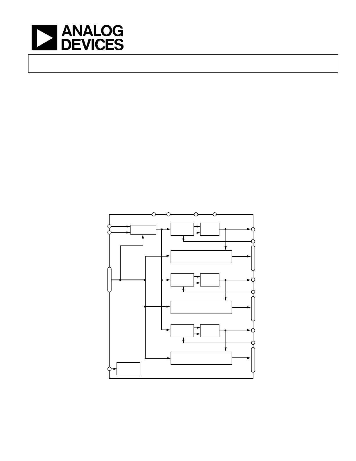
FUNCTIONAL BLOCK DIAGRAM
Delay-Locked Loop
AD8389
PRODUCT DESCRIPTION
The AD8389 is a triple 6-channel LCD microdisplay delaylocked timing loop. As part of a closed-loop system, the AD8389
maintains a constant delay between the common input, DXI,
and each independent feedback reference, MONITxI.
The AD8389 consists of a selectable fixed delay element, a phase
detector, a charge pump, and six matched variable delay lines
per color. The phase detector, charge pump, and master delay
line form a closed loop when connected to a compatible LCD
microdisplay. Five additional delay lines track the master for a
complete set of matched timing signals.
The AD8389 dissipates 40 mW nominal power. The AD8389 is
offered in a 48-lead 7 mm × 7 mm LFCSP package and operates
over the commercial temperature range of 0°C to 85°C.
AVDD(4) AVSS(4) DRVDD(2) DRVSS(2)
COMPEDGE
SLOW
DXI
ENBX1I
ENBX2I
ENBX3I
ENBX4I
CLXI
CLK
DXI
INTERNAL
TIMING
SELECTABLE
DELAY
6
/
PHASE
DETECTOR
MATCHED VARIABLE
DELAY LINES (6-CHANNEL)
PHASE
DETECTOR
MATCHED VARIABLE
DELAY LINES (6-CHANNEL)
PHASE
DETECTOR
MATCHED VARIABLE
DELAY LINES (6-CHANNEL)
CHARGE
PUMP
CHARGE
PUMP
CHARGE
PUMP
Figure 1.
AD8389
6
/
6
/
6
/
VCONTR
MONITRI
DXRO
ENBX1RO
ENBX2RO
ENBX3RO
ENBX4RO
CLXRO
VCONTG
MONITGI
DXGO
ENBX1GO
ENBX2GO
ENBX3GO
ENBX4GO
CLXGO
VCONTB
MONITBI
DXBO
ENBX1BO
ENBX2BO
ENBX3BO
ENBX4BO
CLXBO
04515-0-001
Rev. 0
Information furnished by Analog Devices is believed to be accurate and reliable.
However, no responsibility is assumed by Analog Devices for its use, nor for any
infringements of patents or other rights of third parties that may result from its use.
Specifications subject to change without notice. No license is granted by implication
or otherwise under any patent or patent rights of Analog Devices. Trademarks and
registered trademarks are the property of their respective owners.
One Technology Way, P.O. Box 9106, Norwood, MA 02062-9106, U.S.A.
Tel: 781.329.4700 www.analog.com
Fax: 781.326.8703 © 2003 Analog Devices, Inc. All rights reserved.
Page 2

AD8389
TABLE OF CONTENTS
Specifications..................................................................................... 3
Absolute Maximum Ratings............................................................ 4
Exposed Paddle............................................................................. 4
Maximum Power Dissipation ..................................................... 4
Pin Configuration and Function Descriptions............................. 5
REVISION HISTORY
Revision 0: Initial Version
Timing.................................................................................................6
Operating Principles .........................................................................7
Operation .......................................................................................7
Outline Dimensions..........................................................................9
Ordering Guide .............................................................................9
Rev. 0 | Page 2 of 12
Page 3

AD8389
SPECIFICATIONS
Table 1. @ 25°C, AVDD = DRVDD = 3.3 V, T
Parameter Conditions Min Typ Max Unit
LOGIC INPUTS
C
IN
I
IN
V
IH
V
IL
V
TH
OUTPUTS
V
OH
V
OL
TIMING SPECIFICATIONS
Operating Frequency
CLK, f
CLK
CLXI, ENBX(1–4)I (2t1)
DXI, MONITxI (2t1)
Input Low Pulse Width, t1—All Inputs except CLK
DXI, MONITxI 280 ns
ENBX(1–4)I, CLXI t5 ≤ 230ns 30 ns
CLK High Pulse Width, t
CLK Low Pulse Width, t
CLK to DXI Setup Time, t
Output Rise, Fall Times—tr, t
Delay t
5
Output Skew, t
6
2
3
4
f
t5 ≤ 130 ns 0.3 2.5 ns
t5 ≤ 170ns 0.45 3.4 ns
t5 ≤ 230ns 0.7 5 ns
Loop Delay, t
7
COMPEDGE = H, SLOW = H 9/(f
COMPEDGE = H, SLOW = L 15/(f
COMPEDGE = L, SLOW = H 26/(f
COMPEDGE = L, SLOW = L 32/(f
POWER SUPPLIES
AVDD Operating Range 3 3.6 V
DRVDD Operating Range 3 3.6 V
Total Operating Current f
Power Dissipation f
Operating Temperature 0 85 °C
= 0°C, T
MIN
= 85°C, unless otherwise noted
MAX
pF
–2 +2 µA
2.0 AVDD V
AGND 0.8 V
1.5 V
IO = –2 µA DRVDD – 0.4 V
IO = +2 µA DVRSS + 0.4 V
60 75 85 MHz
–1
–1
Hz
Hz
4.7 ns
4.7 ns
2 ns
CL = 30 pF 5 ns
DXI to DXxO 22 350 ns
CL = 30 pF
) + t
CLK
) + t4 ns
CLK
) + t4 ns
CLK
) + t4 ns
CLK
= 75 MHz, CL = 30 pF 11 mA
CLK
= 75 MHz, CL = 30 pF 40 mW
CLK
ns
4
Rev. 0 | Page 3 of 12
Page 4
AD8389
ABSOLUTE MAXIMUM RATINGS
Table 2. AD8389 Stress Ratings
Parameter Rating
Supply Voltages
AVDDx – AVSSx 3.9 V
DRVDDx – DRVSSx 3.9 V
Input Voltages
Maximum Digital Input Voltage AVDD + 0.3 V
Minimum Digital Input Voltage AVSS – 0.3 V
Internal Power Dissipation
LFCSP Package @ TA = 25°C 4.8 W
Operating Temperature Range 0°C to 85°C
Storage Temperature Range –65°C to +125°C
Lead Temperature Range (Soldering 10 sec) 300°C
1
Stresses above those listed under the Absolute Maximum Ratings may cause
permanent damage to the device. This is a stress rating only; functional
operation of the device at these or any other conditions above those
indicated in the operational section of this specification is not implied.
Exposure to the absolute maximum ratings for extended periods may
reduce device reliability.
2
48-Lead LFCSP Package:
= 26°C/W (JEDEC Standard 4-layer PCB in still air)
θ
JA
= 20°C/W
θ
JC
1
EXPOSED PADDLE
To ensure high reliability, the exposed paddle must be soldered
to GND.
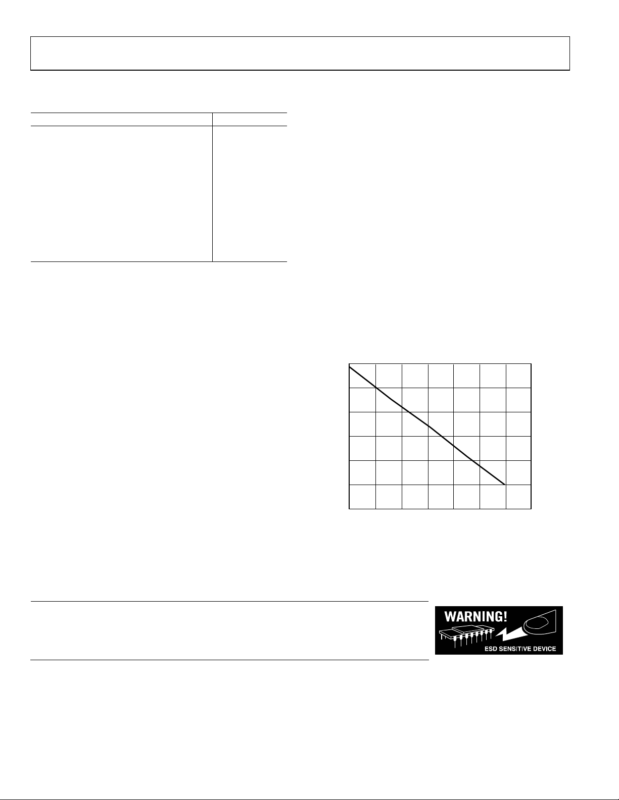
MAXIMUM POWER DISSIPATION
The maximum power that can be safely dissipated by the
AD8389 is limited by its junction temperature. The maximum
2
safe junction temperature for plastic encapsulated devices as
determined by the glass transition temperature of the plastic is
approximately 150°C. Exceeding this limit temporarily may
cause a shift in the parametric performance due to a change in
the stresses exerted on the die by the package. Exceeding a
junction temperature of 175°C for an extended period can
result in device failure.
To ensure operation within the specified operating temperature
range, it is necessary to limit the maximum power dissipation as
follows:
5.0
P
DMAX
= (T
JMAX
– TA)/θ
JA
4.5
4.0
3.5
3.0
POWER DISSIPATION (W)
2.5
2.0
25 35 45 55 65 75 85 95
AMBIENT TEMPERATURE (°C)
Figure 2. Maximum Power Dissipation vs. Ambient Temperature
ESD CAUTION
ESD (electrostatic discharge) sensitive device. Electrostatic charges as high as 4000 V readily
accumulate on the human body and test equipment and can discharge without detection. Although
this product features proprietary ESD protection circuitry, permanent damage may occur on devices
subjected to high energy electrostatic discharges. Therefore, proper ESD precautions are
recommended to avoid performance degradation or loss of functionality.
04515-0-002
Rev. 0 | Page 4 of 12
Page 5

AD8389
V
V
V
PIN CONFIGURATION AND FUNCTION DESCRIPTIONS
AVDD
COMPEDGE
CLXI
ENBX4I
ENBX3I
ENBX2I
ENBX1I
DXI
SLOW
CLK
DRVDD
4847464544
4342414039
DRVSS
38
37
1
AVSS
MONITRI
MONITGI
MONITBI
2
3
4
AVDD
5
AVSS
6
CONTR
7
AVDD
8
AVSS
9
CONTG
10
CONTB
11
AVSS
12
NC =
NO CONNECT
PIN 1
INDICATOR
13NC14NC15
AVDD
AD8389
TOP VIEW
(Not to Scale)
48-LEAD LFCSP
7mm × 7mm
16
17
18
DRVSS
CLXBO
DRVDD
ENBX4BO19ENBX3BO20ENBX2BO21ENBX1BO
22
23
DXBO
24
NC
36
DXRO
35
ENBX1RO
34
ENBX2RO
33
ENBX3RO
32
ENBX4RO
CLXRO
31
30
DXGO
29
ENBX1GO
28
ENBX2GO
27
ENBX3GO
ENBX4GO
26
CLXGO
25
04515-0-003
Figure 3. 48-Lead LFCSP, 7 mm × 7 mm Pin Configuration
Table 3. Pin Function Descriptions
Mnemonic Function Description
AVDD, DRVDD Power Supply Power Supply.
AVSS, DRVSS Ground Ground.
CLK Clock Clock Input. Active edge is the rising edge.
COMPEDGE Edge Select
When set HIGH, the phase detector compares the falling edge of DXIN with the rising edge of
MONITxI. When set LOW, the phase detector compares the rising edge of DXIN with the falling
edge of MONITxI.
SLOW Delay Select
When set HIGH and COMPEDGE = HIGH, the delay between the falling edges of DXI and the
rising edges of MONITI is maintained at 9/(f
) + t4. The delay is maintained at 26/(f
CLK
CLK
COMPEDGE = LOW. When set LOW and COMPEDGE = HIGH, the delay between the falling edges
of DXI and the rising edges of MONITI is maintained at 15/(f
) + t4 with COMPEDGE = LOW.
32/(f
CLK
) + t4. The delay is maintained at
CLK
DXI Reference Input LCD Timing Input from the Image Processor. Used as the input to all phase detectors.
CLXI Input LCD Timing Input from the Image Processor.
ENBX(1–4)I Inputs LCD Timing Inputs from the Image Processor.
MONITxI Feedback Inputs
Inputs from the LCD. Used as the feedback input to each phase detector. When the AD8389
forms part of a closed loop, it maintains a constant delay between the DXI input and this
reference input pin.
DXxO Delayed Outputs
CLXxO Delayed Outputs
ENBX(1–4)xO Delayed Outputs
VCONTx Control Voltage
200 pF capacitors connected between these pins and the AVSS plane are required for proper
operation of the internal charge pump.
) + t4 when
Rev. 0 | Page 5 of 12
Page 6

AD8389
K
TIMING
Table 4. Timing Specifications
Parameter Conditions Min Typ Max Unit
Operating Frequency
CLK, f
CLK
CLXI, ENBX(1–4)I (2t1)
DXI, MONITxI (2t1)
Input Low Pulse Width, t1—All Inputs except CLK
DXI, MONITxI 280 ns
ENBX(1–4)I, CLXI t5 ≤ 230ns 30 ns
CLK High Pulse Width—t
CLK Low Pulse Width—t
CLK to DXI Setup Time—t
2
3
4
Output Rise, Fall Time—tr, tf CL = 30 pF 5 ns
Delay—t
Output Skew— t
5
6
t5 ≤ 130 ns 0.3 2.5 ns
t5 ≤ 170ns 0.45 3.4 ns
t5 ≤ 230ns 0.7 5 ns
Loop Delay, t
7
COMPEDGE = H, SLOW = H 9/(f
COMPEDGE = H, SLOW = L 15/(f
COMPEDGE = L, SLOW = H 26/(f
COMPEDGE = L, SLOW = L 32/(f
t
3
t
2
60 75 85 MHz
–1
Hz
–1
Hz
4.7 ns
4.7 ns
2 ns
DXI to DXxO 22 350 ns
CL = 30 pF
) + t
CLK
4
) + t
CLK
4
) + t
CLK
4
) + t
CLK
4
DXI
ns
ns
ns
ns
CL
DXI
t
4
t
1
Figure 4. CLK and DXI Timin g
V
TH
t
4
V
TH
04515-0-004
MONITxI
DXO
DXxO
CLXxO
ENBX(1–4)XO
t
7
t
t
5
EXT
t
6
04515-0-005
Figure 5. Input and Output Waveforms at COMPEDGE = HIGH
Rev. 0 | Page 6 of 12
Page 7

AD8389
OPERATING PRINCIPLES
MON
MONITRI
DX
CLX,
ENBX(1–4)
200pF
DXI
VCONTR
DXRO
CLXRO,
ENBX(1–4)O
AD8389
Figure 6. AD8389 Application in the Red Channel of an LCD Projection System
The image quality of an LCD system is dependent on the timing
relationship between the control inputs, DX, CLX, ENBX(1–4),
and the video channels.
TFT delay and switching speed variations, due to temperature
variations and LCD aging, degrade image quality if not
compensated.
An internal reference TFT connected to an internal pull-up
resistor, as shown in Figure 6, characterizes the internal S/H
TFTs of the LCD and monitors switching speed and delay
variations due to aging and temperature. When the MON
output of an LCD that includes such an internal reference TFT
is connected to the reference input of the AD8389 delay-locked
timing loop, continuously optimized timing of the LCD is
maintained automatically.
MONITO
DXI DXO
ENBX(1–4)I ENBX(1–4)O
AD8384/AD8385
LEVEL SHIFTER SECTION
MONITI
CLXO,CLXIN,
OPERATION
As part of a closed loop, the AD8389 maintains a constant delay
between the common input, DXI, and each independent
feedback reference, MONITxI. The block diagram of such
closed-loop system is shown in Figure 6.
A constant delay, t
control inputs, is applied to the DXI input to approximate the
nominal, initially expected total delay, t
shifters and the LCD as shown in Table 5.
Table 5
COMPEDGE SLOW Constant Delay
1 0 15/f
1 1 9/f
H SHIFT
REGISTER
RED LCD
04515-0-006
, selected via the COMPEDGE and SLOW
7
, through the level
7
DX
4
4
MONITRI
CONSTANT
CLK
CLK
+ t
+ t
0 0 32/f
0 1 26/f
CLK
CLK
+ t
+ t
DX
MONITRI
CONSTANT
4
4
Rev. 0 | Page 7 of 12
Page 8

AD8389
The phase detector compares the delayed DX and MONITxI
reference inputs and automatically adjusts the variable delay (t
maintaining the constant delay (t
) between the active edges of
7
DX and MONITxI. Five matched delay lines maintain the phase
relationship between DXxO, CLXxO, and ENBX(1–4)xO.
5
CLK
),
DX
MONITRI
CONSTANT
When the loop is locked, t
= t5 + t
7
, where t
EXT
is the total
EXT
delay through the level shifter and the LCD.
The external delay of a typical system is the sum of the level
shifter delay (20 ns typical) and the LCD delay, (typically in the
range of 20 ns to 120 ns). At a 75 MHz operating clock
frequency, the maximum expected total delay of 140 ns is equal
to 10.5 clock cycles, requiring COMPEDGE = 1, SLOW = 0 for
systems using negative active edge for DX.
CLX
ENBX1
AD8389 INPUTS
ENBX2
ENBX3
ENBX4
DXO
MONITI
CLXO
ENBX1O
LCD INPUTS AND OUTPUT
ENBX2O
ENBX3O
ENBX4O
04515-0-007
Figure 7. Typical Input Waveforms at the AD8389 and at the LCD.
COMPEDGE = HIGH .
Rev. 0 | Page 8 of 12
Page 9

AD8389
OUTLINE DIMENSIONS
0.30
0.23
0.18
PIN 1
48
INDICATOR
1
BSC SQ
PIN 1
INDICATOR
7.00
0.60 MAX
37
36
0.60 MAX
5.25
5.10 SQ
4.95
12
13
0.25 MIN
1.00
0.85
0.80
12° MAX
SEATING
PLANE
TOP
VIEW
0.80 MAX
0.65 TYP
0.50 BSC
COMPLIANT TO JEDEC STANDARDS MO-220-VKKD-2
6.75
BSC SQ
0.20 REF
0.50
0.40
0.30
0.05 MAX
0.02 NOM
COPLANARITY
25
0.08
BOTTOM
VIEW
24
5.50
REF
Figure 8. 48-Lead Frame Chip Scale Package [LFCSP] (CP-48)
ORDERING GUIDE
Model Temperature Range Package Description Package Option
AD8389ACPZ
1
Z = lead-free.
1
0°C to 85°C 48-Lead Lead Frame Chip Scale Package CP-48
Rev. 0 | Page 9 of 12
Page 10

AD8389
NOTES
Rev. 0 | Page 10 of 12
Page 11

AD8389
NOTES
Rev. 0 | Page 11 of 12
Page 12

AD8389
NOTES
© 2003 Analog Devices, Inc. All rights reserved. Trademarks and
registered trademarks are the property of their respective owners.
D04515–0–10/03(0)
Rev. 0 | Page 12 of 12
 Loading...