

Page 1
High Performance, 12-Bit, 12-Channel
FEATURES
High accuracy, high-resolution voltage outputs
1 mV channel matching
12-bit input resolution
Laser-trimmed outputs
Fast settling, high voltage drive
35 ns settling time to 0.25% into 150 pF load
Slew rate 420 V/μs
Outputs to within 1.3 V of supply rails
High update rates
Fast, 110 MHz clock
Programmable video reference (brightness) and
full-scale (contrast) output levels
Flexible logic
INV bit reverses polarity of video signal
R/L reverses loading order of data
ISW selects frame/row or column/dot inversion
DSW selects single or dual data bus mode
Output short-circuit protection
3.3 V logic, 11 V to 18 V analog supplies
Available in 80-lead, 12 mm × 12 mm, TQFP E-pad
APPLICATIONS
LCD microdisplay driver
GENERAL DESCRIPTION
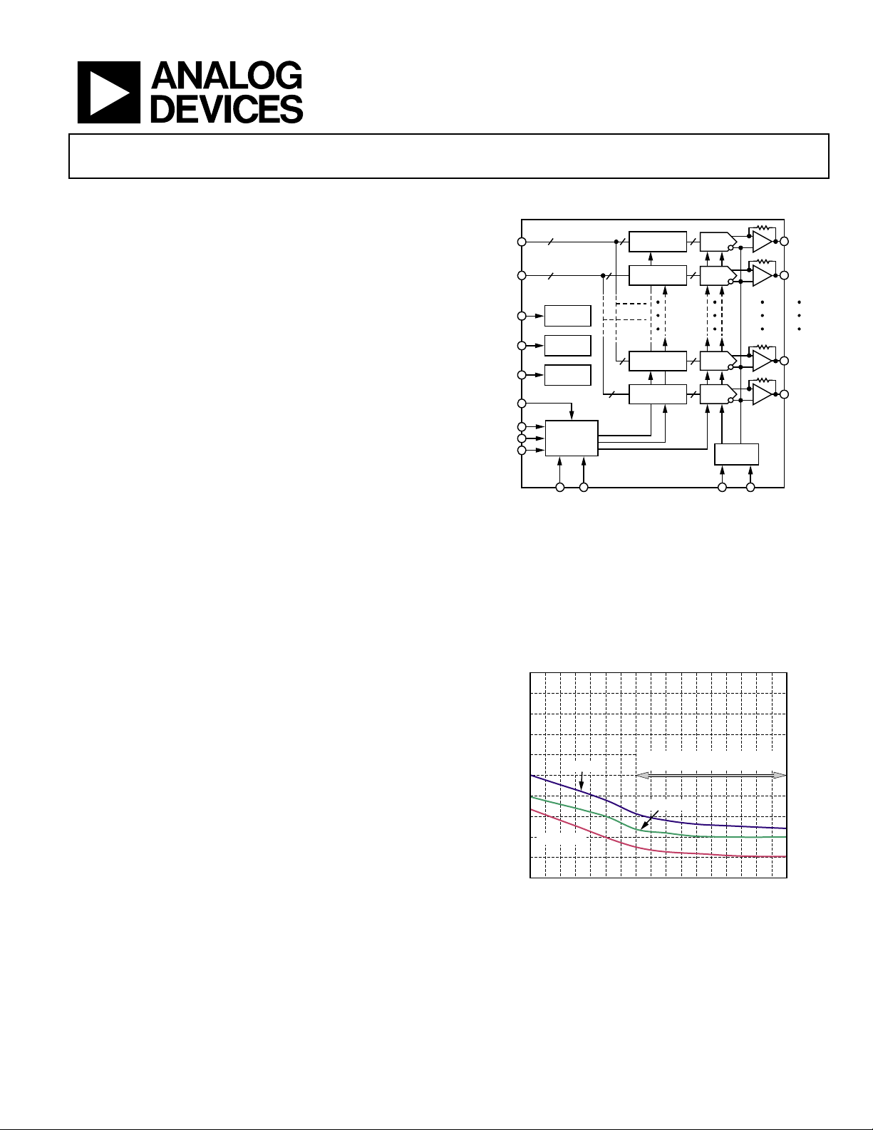
The AD8387 DecDriver provides dual, fast latched, 12-bit
decimating input, which drives 12 high voltage outputs. Twelvebit input words are loaded into 12 separate high speed, bipolar
DACs sequentially. Flexible digital input format allows more
than one AD8387 to be used in parallel for higher resolution
displays. The output signal can be adjusted for dc reference,
signal inversion, and contrast for maximum flexibility.
The AD8387 is fabricated on ADI’s fast bipolar, 26 V XFCB
process, providing fast input logic, bipolar DACs with trimmed
accuracy and fast settling, high voltage, precision drive
amplifiers on the same chip.
The AD8387 dissipates 1.34 W nominal static power. The
AD8387 is offered in an 80-lead TQFP E-pad package and
operates over the commercial temperature range of 0°C to
+85°C.
Decimating, LCD DecDriver
AD8387
FUNCTIONAL BLOCK DIAGRAM
DBA(0:11)
DBB(0:11)
BYP
TSW
GSW
DSW
CLK
XFR
R/L
ΔVDE CHANNEL MATCHING (mV)
12
12 12
BIAS
THERMAL
SWITCH
G-MODE
SWITCH
SEQUENCE
CONTROL
5
4
3
2
1
0
CODE 0
CODE 4095
0
10 20 30 40 50 60 70 80
INTERNAL AMBIENT TEMPERATURE (°C)
Figure 2. Channel Matching vs. Temperature
12 12
12
12
TWO-STAGE
LATCH
TWO-STAGE
LATCH
TWO-STAGE
LATCH
TWO-STAGE
LATCH
AD8387
DAC
12
DAC
12
DAC
12
DAC
Figure 1.
NORMAL PROJECTOR OPERATING
TEMPERATURE RANGE
CODE 2048
SCALING
CONTROL
VRLVRHISWINV
VID0
VID1
VID10
VID11
05653-015
®
05653-001
Rev. 0
Information furnished by Analog Devices is believed to be accurate and reliable. However, no
responsibility is assumed by Anal og Devices for its use, nor for any infringements of patents or ot her
rights of third parties that may result from its use. Specifications subject to change without notice. No
license is granted by implication or otherwise under any patent or patent rights of Analog Devices.
Trademarks and registered trademarks are the property of their respective owners.
One Technology Way, P.O. Box 9106, Norwood, MA 02062-9106, U.S.A.
Tel: 781.329.4700 www.analog.com
Fax: 781.461.3113 © 2005 Analog Devices, Inc. All rights reserved.
Page 2

AD8387
TABLE OF CONTENTS
Features .............................................................................................. 1
Theory of Operation ...................................................................... 13
Applications....................................................................................... 1
Functional Block Diagram .............................................................. 1
General Description ......................................................................... 1
Revision History ............................................................................... 2
Specifications..................................................................................... 3
Absolute Maximum Ratings............................................................ 5
Exposed Paddle............................................................................. 5
Overload Protection ..................................................................... 5
Maximum Power Dissipation ..................................................... 5
Operating Temperature Range ................................................... 5
ESD Caution.................................................................................. 5
Pin Configuration and Function Descriptions............................. 6
Typical Performance Characteristics ............................................. 8
Timing Diagrams.............................................................................. 9
Single Data Bus Configuration, DSW = LOW ......................... 9
Transfer Function and Analog Output Voltage...................... 13
Accuracy ...................................................................................... 13
Applications..................................................................................... 14
Optimized Reliability with the Thermal Switch .................... 14
Initial Power-Up After Assembly or Repair............................ 14
Power-Up During Normal Operation ..................................... 14
Power Supply Sequencing ......................................................... 14
Power-On Sequence ................................................................... 14
Power-Off Sequence................................................................... 14
Grounded Output Mode During Power-Off .......................... 14
PCB Design for Optimized Thermal Performance ............... 14
Thermal Pad Design .................................................................. 15
Thermal via Structure Design .................................................. 15
AD8387 PCB Design Recommendations ............................... 15
Outline Dimensions ....................................................................... 16
Dual Data Bus Configuration, DSW = HIGH........................ 10
Functional Description ..................................................................12
Reference and Control Input Description............................... 12
REVISION HISTORY
10/05—Revision 0: Initial Version
Ordering Guide .......................................................................... 16
Rev. 0 | Page 2 of 16
Page 3

AD8387
SPECIFICATIONS
TA = 25°C, AVCC = 15.5 V, DVCC = 3.3 V, VRH = 9.5 V, VRL = 7 V, T
Table 1.
Parameter Conditions Min Typ Max Unit
VIDEO DC PERFORMANCE
1
T
A MIN
to T
,VFS = 5 V
A MAX
VDE—Differential Error Voltage @ DAC code 0 −5.5 −0.8 +5.0 mV
@ DAC code 1024 −4.4 −0.5 +3.6 mV
@ DAC code 2048 −3.6 −0.3 +3.3 mV
@ DAC code 3072 −2.8 −0.3 +2.8 mV
@ DAC code 4095 −2.1 +0.2 +2.1 mV
DAC code range 0 to 4095 −6.0 +6.0 mV
VCME—Common-Mode Error Voltage @ DAC code 0 −2.5 −0.3 +2.5 mV
@ DAC code 1024 −2.5 −0.3 +2.5 mV
@ DAC code 2048 −2.5 −0.3 +2.5 mV
@ DAC code 3072 −2.5 −0.3 +2.5 mV
@ DAC code 4095 −2.5 −0.3 +2.5 mV
DAC code range 0 to 4095 −3.5 +3.5 mV
ΔVDE—VDE Channel Matching @ DAC code 0 1.9 4.8 mV
@ DAC code 1024 1.8 4.3 mV
@ DAC code 2048 1.6 4.0 mV
@ DAC code 3072 1.4 3.8 mV
@ DAC code 4095 1.0 2.8 mV
DAC code range 0 to 4095 5.5 mV
ΔV—Channel Matching @ DAC code 0 2.7 mV
@ DAC code 1024 2.7 mV
@ DAC code 2048 2.5 mV
@ DAC code 3072 2.5 mV
@ DAC code 4095 2.0 mV
DAC code range 0 to 4095 7.5 mV
2
DNL
VIDEO OUTPUT DYNAMIC PERFORMANCE T
−1 −0.2 LSB
to T
A MIN
A MAX
Data Switching Settling Time to 0.25% VIDx = 5 V step, CL = 150 pF 35 50 ns
Data Switching Settling Time to 1% 22 28 ns
Data Switching Slew Rate 20% to 80% 420 V/μs
CLK and Data Feedthrough
All-Hostile Crosstalk
3
4
15 mV p-p
Amplitude 69 mV p-p
Glitch Duration 50 ns
DAC Transition Glitch Energy DAC Code 2047 to 2048 0.4 nV-s
Invert Switching Settling Time to 0.25% VIDx = 10 V step, CL = 150 pF 70 150 ns
Invert Switching Settling Time to 1% 34 40 ns
Invert Switching Slew Rate 20% to 80% 700 V/μs
Invert Switching Overshoot 25 mV
Rev. 0 | Page 3 of 16
A MIN
= 0°C, T
= 75°C still air, unless otherwise noted.
A MAX
Page 4

AD8387
Parameter Conditions Min Typ Max Unit
VIDEO OUTPUT CHARACTERISTICS
Output Voltage Swing AVCC − VOH, VOL − AGND 0.9 1.3 V
Output Voltage—Grounded Mode 0.06 0.150 V
Data Switching Delay: t
Data Switching Delay Skew: Δt
INV Switching Delay: t
INV Switching Delay Skew: Δt
Output Current 100 mA
Output Resistance 28 Ω
REFERENCE INPUTS
VRL Range VRH ≥ VRL 5.25 AVCC − 4 V
VRH Range VRH ≥ VRL VRL VRL + 2.75 V
VRH to VRL Range
VRH Input Resistance To VRL 22 kΩ
VRL Input Current −44 μA
VRH Input Current 111 μA
RESOLUTION Binary Coding 12 Bits
DIGITAL INPUT CHARACTERISTICS
CLK Frequency DSW = HIGH 110 MHz
DSW = LOW 85 MHz
Data Setup Time: t1 0 ns
XFR Setup Time: t3 0 ns
Data Hold Time: t2 3.5 ns
XFR Hold Time: t4 3.5 ns
CLK High Time: t5 DSW = HIGH 2.5 ns
CLK Low Time: t6 DSW = HIGH 3.0 ns
CLK High Time: t7 DSW = LOW 3.5 ns
CLK Low Time: t8 DSW = LOW 4.0 ns
CIN 3 pF
IIH 0.05 μA
IIH TSW 333 μA
IIH XFR 0.05 μA
IIL −0.6 μA
IIL TSW −1.3 μA
IIL XFR −1.2 μA
VIH 2 V
VIL 0.8 V
VTH 1.65 V
POWER SUPPLIES
DVCC, Operating Range 3 3.3 3.6 V
DVCC, Quiescent Current 54 70 mA
AVCC, Operating Range 11 18 V
AVCC, Quiescent Current 75 100 mA
OPERATING TEMPERATURE
Ambient Temperature Range, T
Ambient Temperature Range, T
1
VDE = differential error voltage, VCME = common-mode error voltage, ΔVDE = VDE matching between outputs, ΔV = maximum deviation between outputs, and full-scale output
voltage = VFS = 2 × (VRH − VRL). See the Accuracy section.
2
Guaranteed monotonic by characterization to four sigma limits.
3
Measured on two outputs differentially as CLK and DBx(0:11) are driven and XFR is held LOW.
4
Measured on two outputs differentially as the others are transitioning by 5 V. Measured for both states of INV.
5
Measured from 50% of rising CLK edge to 50% of output change. Measurement is made for both states of INV.
6
Measured from 50% of INV transition to 50% of output change.
7
Operation at elevated ambient temperature requires a thermally optimized PCB and additional thermal management, such as airflow across the surface of the AD8387.
5
7
6
8
1
5
7
6
8
VIDx = 5 V step 15.7 ns
4 ns
VIDx = 10 V step 16.2 ns
4 ns
0 2.75 V
T
A MIN
to T
A MAX
CLK input duty cycle 40% to 60%
7
A
7
A
Still air, TSW = LOW 0 75 °C
200 lfm airflow, TSW = LOW 0 85 °C
Rev. 0 | Page 4 of 16
Page 5
AD8387
ABSOLUTE MAXIMUM RATINGS
Table 2.
Parameter Rating
Supply Voltages
AVCCx − AGNDx 18 V
DVCC − DGND 4.5 V
Input Voltages
Maximum Digital Input Voltage DVCC + 0.5 V
Minimum Digital Input Voltage DGND − 0.5 V
Maximum Analog Input Voltage AVCC + 0.5 V
Minimum Analog Input Voltage AGND − 0.5 V
Internal Power Dissipation
1
TQFP E-Pad @ TA = 25°C 4.38 W
Operating Temperature Range 0°C to 85°C
Storage Temperature Range −65°C to +125°C
Lead Temperature Range (Soldering 10 sec) 300°C
1
80-lead TQFP E-Pad:
θJA = 28.5°C/W (still air) [JEDEC Standard, 4-layer PCB in still air]
θJC = 12.2°C/W
θJB = 14.6°C/W
ΨJB = 12.0°C/W
ΨJT = 0.3°C/W.
Stresses above those listed under the Absolute Maximum
Ratings may cause permanent damage to the device. This is a
stress rating only; functional operation of the device at these or
any other conditions above those indicated in the operational
section of this specification is not implied. Exposure to the
absolute maximum ratings for extended periods may reduce
device reliability.
EXPOSED PADDLE
To ensure optimized thermal performance, the exposed paddle
must be thermally connected to an external plane, such as
AVCC or GND, as described in the
Applications section.
OVERLOAD PROTECTION
The AD8387 overload protection circuit consists of an output
current limiter and a thermal switch.
When TSW is LOW, the thermal switch is disabled and the
output current limiter is enabled. The maximum current at any
one output is internally limited to 100 mA average. In the event
of a momentary short-circuit between a video output and a
power supply rail (VCC or AGND), the output current limit is
sufficiently low to provide temporary protection.
When TSW is HIGH, the output current limiter, as well as the
thermal switch, is enabled. The thermal switch debiases the
output amplifier when the junction temperature reaches the
internally set trip point. In the event of an extended shortcircuit between a video output and a power supply rail, the
output amplifier current continues to switch between 0 and
100 mA typical with a period determined by the thermal time
constant and the hysteresis of the thermal trip point. The
thermal switch, when enabled, provides long-term protection
from accidental shorts during the assembly process by limiting
the average junction temperature to a safe level.
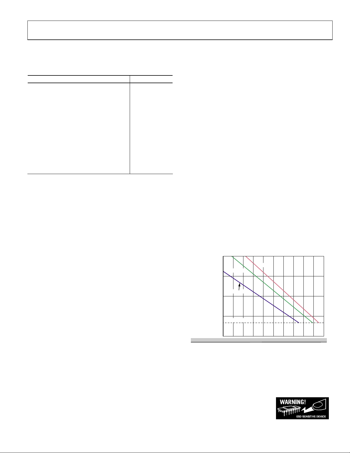
MAXIMUM POWER DISSIPATION
The maximum power that the AD8387 can safely dissipate is
limited by its junction temperature. The maximum safe junction
temperature for plastic encapsulated devices, as determined by the
glass transition temperature of the plastic, is approximately 150°C.
Exceeding this limit temporarily can cause a shift in the parametric
performance due to a change in the stresses exerted on the die by
the package. Exceeding a junction temperature of 150°C for an
extended period can result in device failure.
OPERATING TEMPERATURE RANGE
To ensure operation within the specified operating temperature
range, it is necessary to limit the maximum power dissipation as
follows.
3.0
200LFM
2.5
STILL AIR
2.0
1.5
QUIESCENT
MAXIMUM POWER DISSIPATION (W)
THERMAL
SWITCH
ENABLED
DISABLED
AD8387 on a 4-Layer JEDEC PCB with Thermally Optimized Landing
1.0
50 55 60 65 70 75 80 85 90 10095
75 80 85 90 95 100 105 110 115 125120
Figure 3. Maximum Power Dissipation vs. Temperature,
Pattern as Described in the
500LFM
AMBIENT TEMPERATURE (°C)
Applications Section
05653-002
ESD CAUTION
ESD (electrostatic discharge) sensitive device. Electrostatic charges as high as 4000 V readily accumulate on
the human body and test equipment and can discharge without detection. Although this product features
proprietary ESD protection circuitry, permanent damage may occur on devices subjected to high energy
electrostatic discharges. Therefore, proper ESD precautions are recommended to avoid performance
degradation or loss of functionality.
Rev. 0 | Page 5 of 16
Page 6

AD8387
PIN CONFIGURATION AND FUNCTION DESCRIPTIONS
DBA479DBA378DBA277BBA176DBA075DVCC274DGND273NC72NC71NC70AGNDD69AGNDD68AVCCD67AVCCD66VRH65VRH64VRL63AGND062VID061AVCC0, 1
80
1
DBA5
2
DBA6
3
DBA7
4
DBA8
5
DBA9
XFR
CLK
DSW
R/L
DBB9
DBB8
DBB7
DBB6
DBB5
6
7
8
9
10
11
12
13
14
15
16
17
18
19
20
DBA10
DBA11
DVCC1
DGND1
DBB11
DBB10
NC = NO CONNECT
PIN 1
21
DBB422DBB323DBB224DBB125DBB0
Figure 4. 80-Lead TQFP E-Pad Pin Configuration
26
DVCC3
27
DGND3
28
AD8387
TOP VIEW
(Not to Scale)
29
30
31
INV
ISW
GSW
32
TSW
AGNDB33AGNDB
34
AVCCB35AVCCB
36
37
BYP
38NC39
TSTA
60
VID1
59
AGND1, 2
58
VID2
57
AVCC2, 3
56
VID3
55
AGND3, 4
54
VID4
53
AVCC4, 5
52
VID5
51
AGND5, 6
50
VID6
49
AVCC6, 7
48
VID7
47
AGND7, 8
46
VID8
45
AVCC8, 9
44
VID9
43
AGND9, 10
42
VID10
41
AVCC10, 11
40
VID11
AGND11
05653-004
Rev. 0 | Page 6 of 16
Page 7

AD8387
Table 3. 80-Lead TQFP E-Pad Pin Configurations
Pin No. Mnemonic Function Description
1 to 7,
76 to 80;
14 to 25 DBB(0:11) Data Input 12-Bit Data Input for Odd Channels. VID(1, 3, 5, 7, 9, 11), MSB = DBB11.
8 XFR Transfer/Start Sequence
9, 26, 75 DVCCx Digital Power Supplies Digital Power Supplies.
10, 27, 74 DGNDx Digital Ground These pins are normally connected to the digital ground plane.
11 CLK Clock Clock Input.
12 DSW Data Mode Switch Selects Single Buss or Dual Buss Operating Modes.
13 R/L Right/Left Select Selects Left Direction or Right Direction Operating Mode.
28 ISW Invert Mode Switch Enables and Disables Column Inversion.
29 INV Invert Changes the Polarity of the Analog Output Signals.
30 GSW Output Mode Switch Enables and Disables Grounded Mode.
31 TSW Thermal Switch Enables and Disables Long-Term Output Protection.
32, 33, 39, 43,
47, 51, 55, 59,
63, 69, 70
34, 35, 41,
45, 49, 53,
57, 61, 67, 68
36 BYP Bypass
37 TSTA Test Pin Connect This Pin to AGND.
38, 71 to 73 NC NC No Connect. No internal connection.
40, 42, 44, 46,
48, 50, 52, 54,
56, 58, 60, 62
64 VRL Video Center Reference
65, 66 VRH Full-Scale Reference
DBA(0:11) Data Input 12-Bit Data Input for Even Channels. VID(0, 2, 4, 6, 8, 10), MSB = DBA11.
Simultaneously initiates a new data loading sequence and transfers data
loaded previously, to the outputs.
AGNDx Analog Ground Analog Supply Returns.
AVCCx Analog Power Supplies Analog Power Supplies.
A 0.1 μF capacitor connected between BYP and AGND ensures optimum
settling time.
VID0 to VID11 Analog Outputs These pins are connected directly to the analog inputs of the LCD panel.
This Voltage Sets the Video Center Voltage. The video outputs are above
this reference while INV = HIGH and below this reference while INV = LOW.
Twice the voltage applied between VRH and VRL sets the full-scale
video output voltage.
Rev. 0 | Page 7 of 16
Page 8

AD8387
TYPICAL PERFORMANCE CHARACTERISTICS
5.0
4.5
4.0
3.5
3.0
2.5
2.0
1.5
CHANNEL MATCHING (mV)
1.0
0.5
0
0 4096
512 1024 1536 2048 2560 3072 3584
INPUT CODE
Figure 5. Channel Matching vs. Code @ T
ΔVP
= 25°C
A
5
4
3
2
1
0
VDE (mV)
–1
–2
–3
–4
–5
0 4096
512 1024 1536 2048 2560 3072 3584
INPUT CODE
Figure 6. VDE vs. Code
1.0
0.8
0.6
0.4
0.2
0
DNL (LSB)
–0.2
–0.4
–0.6
–0.8
–1.0
0 4096
512 1024 1536 2048 2560 3072 3584
INPUT CODE
Figure 7. DNL vs. Code @ TA = 25°C, INV = H
ΔVDE
ΔVN
05653-016
05653-018
05653-017
5.0
4.5
4.0
3.5
3.0
2.5
2.0
1.5
1.0
ΔVDE CHANNEL MATCHING (mV)
0.5
0
CODE 0
CODE 2048
CODE 4095
0
10 20 30 40 50 60 70 80
AMBIENT TEMPERATURE (°C)
Figure 8. Channel Matching vs. TA @ Codes 0, 2048, 4095
3.5
2.5
1.5
0.5
–0.5
VCME (mV)
–1.5
–2.5
–3.5
0 4096
512 1024 1536 2048 2560 3072 3584
INPUT CODE
Figure 9. VCME vs. Code
1.0
0.8
0.6
0.4
0.2
0
DNL (LSB)
–0.2
–0.4
–0.6
–0.8
–1.0
0 4096
512 1024 1536 2048 2560 3072 3584
Figure 10. DNL vs. Code @ T
INPUT CODE
A
= 25°C, INV = L
05653-019
05653-021
05653-020
Rev. 0 | Page 8 of 16
Page 9

AD8387
TIMING DIAGRAMS
SINGLE DATA BUS CONFIGURATION, DSW = LOW
12
REFERENCES
VRH
VRL
PIXEL
CLK
PROCESSOR
÷2
IMAGE
D(0:11)
CLK
XFR
R/L
INV
Figure 11. AD8387 in Single Data Bus System
LEFT RIGHT
PIXEL CLK PIXEL CLK
–
3
–1–
D(0:11) D(0:11)
INPUTS
2
CLK CLK
XFR XFR
R/L R/L
DBA(0:11)
DBB(0:11)
CLK
XFR
R/L
INV
DSW
ISW
VRH
VRL
INPUTS
AD8387
–
30 01 12 23 34 45 56 67 78 89 910 1011 1113 1314 1415 1516 1617 1718 1819 1920 2021 2122 2223 2324 2412
12-CHANNEL
LCD
VID0
VID1
VID2
VID3
VID4
VID5
VID6
VID7
VID8
VID9
VID10
VID11
–1–
2
CHANNEL 0
CHANNEL 1
CHANNEL 2
CHANNEL 3
CHANNEL 4
CHANNEL 5
CHANNEL 6
CHANNEL 7
CHANNEL 8
CHANNEL 9
CHANNEL 10
CHANNEL 11
12
05653-005
120–12VID0
131–11VID1
142–10VID2
153–9VID3
164–8VID4
175–7VID5
OUTPUTS
186–6VID6
OUTPUTS
197–5VID7
208–4VID8
219–3VID9
2210–2VID10
2311–1VID11
2311–1VID0
2210–2VID1
219–3VID2
208–4VID3
197–5VID4
186–6VID5
175–7VID6
164–8VID7
153–9VID8
142–10VID9
131–11VID10
120–12VID11
05653-006
Figure 12. AD8387 in Single Data Bus Configuration Scanning Left-to-Right and Right-to-Left
Rev. 0 | Page 9 of 16
Page 10
AD8387
DUAL DATA BUS CONFIGURATION, DSW = HIGH
INPUTSOUTPUTS
PIXEL CLK
DBA(0:11)
DBB(0:11)
CLK
XFR
–2 120
–1 131
2
3
PIXEL
CLK
PROCESSOR
64
75
÷2
IMAGE
DA(0:11)
DB(0:11)
CLK
XFR
R/L
INV
LEFT
108
119
12
12
DVCC
REFERENCES
VRH
VRL
Figure 13. AD8387 in Dual Data Bus System
14
1816
222324
20
15
1917
25
21
DBA(0:11)
DBB(0:11)
CLK
XFR
R/L
INV
DSW
ISW
VRH
VRL
PIXEL CLK
DBA(0:11)
DBB(0:11)
INPUTSOUTPUTS
VID0
VID1
VID2
AD8387
CLK
XFR
VID3
VID4
VID5
VID6
VID7
VID8
VID9
VID10
VID11
–1 131
–2 0 12
CHANNEL 0
CHANNEL 1
CHANNEL 2
CHANNEL 3
CHANNEL 4
CHANNEL 5
CHANNEL 6
CHANNEL 7
CHANNEL 8
CHANNEL 9
CHANNEL 10
CHANNEL 11
3
2
12-CHANNEL
LCD
RIGHT
75
119
64
108
05653-007
15
14
1917
1816
25
21
222324
20
R/L
120–12VID0
131–11VID1
142–10VID2
153–9VID3
164–8VID4
175–7VID5
186–6VID6
197–5VID7
208–4VID8
219–3VID9
2210–2VID10
2311–1VID11
R/L
2311–1VID0
2210–2VID1
219–3VID2
208–4VID3
197–5VID4
186–6VID5
175–7VID6
164–8VID7
153–9VID8
142–10VID9
131–11VID10
120–12VID11
05653-008
Figure 14. AD8387 in Dual Data Bus Configuration Scanning Left-to-Right and Right-to-Left
Rev. 0 | Page 10 of 16
Page 11

AD8387
V
t
6
CLK
t
5
t
1
t
2
t
1
t
2
V
TH
DB(0:11)
XFR
V
t
3
t
4
TH
V
TH
05653-009
Figure 15. Input Timing (DSW = LOW)
CLK
–2 15
DB(0:11)
XFR
ID(0:11)
–12, –11, –10, –9, –8, –7, –6, –5, –4, –3, –2, –1
–1 1 2 3 4 5 6 7 8 9 10 11 13 14
INV
VRL + VFS
50%
VRL
t
7
PIXELS
t
8
120
t
7
0, 1, 2, 3, 4, 5, 6, 7, 8, 9, 10, 11
PIXELS
VRL–VFS
VRL
05653-010
Figure 16. Output Timing (DSW = LOW)
Table 4.
Parameter Conditions Min Typ Max Unit
Data Setup Time: t1 0 ns
XFR Setup Time: t3 0 ns
Data Hold Time: t2 3.5 ns
XFR Hold Time: t4 3.5 ns
CLK High Time: t5 DSW = HIGH 2.5 ns
CLK Low Time: t6 DSW = HIGH 3.0 ns
CLK High Time: t7 DSW = LOW 3.5 ns
CLK Low Time: t8 DSW = LOW 4.0 ns
Data Switching Delay: t
7
Data Switching Delay Skew: Δt
Invert Switching Delay: t
8
Invert Switching Delay Skew: Δt
7
8
15.7 ns
VIDx = 5 V step 4 ns
16.2 ns
4 ns
Rev. 0 | Page 11 of 16
Page 12

AD8387
FUNCTIONAL DESCRIPTION
The AD8387 is a system building block designed to directly
drive the columns of LCD microdisplays of the type popularized
for use in projection systems. It has 12 channels of precision,
12-bit DACs loaded from a dual, high speed, 12-bit wide input.
Precision current feedback amplifiers, providing well damped
pulse response and fast voltage settling into large capacitive
loads, buffer the 12 outputs. Laser trimming at the wafer level
ensures low absolute output errors and tight channel-to-channel
matching. Tight part-to-part matching in high resolution
systems is guaranteed by the use of external voltage references.
REFERENCE AND CONTROL INPUT DESCRIPTION
Data Transfer/Start Sequence Control—Input Data Loading, Data Transfer
A valid XFR is initiated when it is held HIGH during a rising
CLK edge.
Data is transferred to the outputs and a new loading sequence is
initiated on the next rising CLK edge, immediately following a
valid XFR.
During a loading sequence, 12-bit words are loaded sequentially
into 12 internal channels.
When the AD8387 is configured for single data bus (DSW =
LOW), data is loaded on both the rising and falling edges of
CLK. When configured for dual data bus (DSW = HIGH),
data is loaded on the rising edges of CLK only.
DSW Control—Data Mode Switch
When this input is HIGH, the AD8387 is in dual data bus
mode. Data is loaded from both DBA(0:11) and DBB(0:11)
on the rising CLK edge simultaneously. R/L does not change
the active CLK edge in dual data bus mode. When LOW, the
AD8387 is in single data bus mode. Data is loaded on the rising
CLK edge from DBA(0:11) and on the falling CLK edge from
DBB(0:11) when R/L is LOW. With R/L HIGH, data is loaded
on the falling CLK edge from DBA(0:11) and on the rising CLK
edge from DBB(0:11).
Right/Left Control—Input Data Loading
To facilitate image mirroring, the direction of the loading
sequence is set by the R/L control. A new loading sequence
begins at Channel 0 and proceeds to Channel 11 when the R/L
control is held LOW. It begins at Channel 11 and proceeds to
Channel 0 when the R/L control is held HIGH.
TSW Control—Thermal Switch Control
When this input is HIGH, the thermal switch is enabled. When
LOW or left unconnected, the thermal switch is disabled.
An internal, 10 kΩ pull-down resistor disables the thermal
switch when this pin is left unconnected.
GSW Control—Output Mode Switch
When this input is HIGH, the video outputs operate normally.
When LOW or left open, the video outputs are forced to
AGND. This function operates when AVCC power is off but
requires DVCC power to be on.
INV Control and ISW Control—Analog Output Inversion
When ISW = LOW, the analog outputs’ transfer function is
below VRL, while INV is held LOW, and is above VRL, while
INV is held HIGH.
With ISW = HIGH, the analog outputs’ transfer function is
above VRL for VID(0, 2, 4, 6, 8, 10) and is below VRL for
VID(1, 3, 5, 7, 9, 11), while INV is held HIGH. Conversely, the
analog outputs’ transfer function is below VRL for VID(0, 2, 4,
6, 8, 10) and is above VRL for VID(1, 3, 5, 7, 9, 11), while INV is
held LOW.
VRH, VRL Inputs—Full-Scale Video Reference Inputs
Two times the difference between VRH and VRL (analog input
voltages) sets the full-scale output voltage.
VFS = 2 × (VRH − VRL)
Rev. 0 | Page 12 of 16
Page 13
AD8387
THEORY OF OPERATION
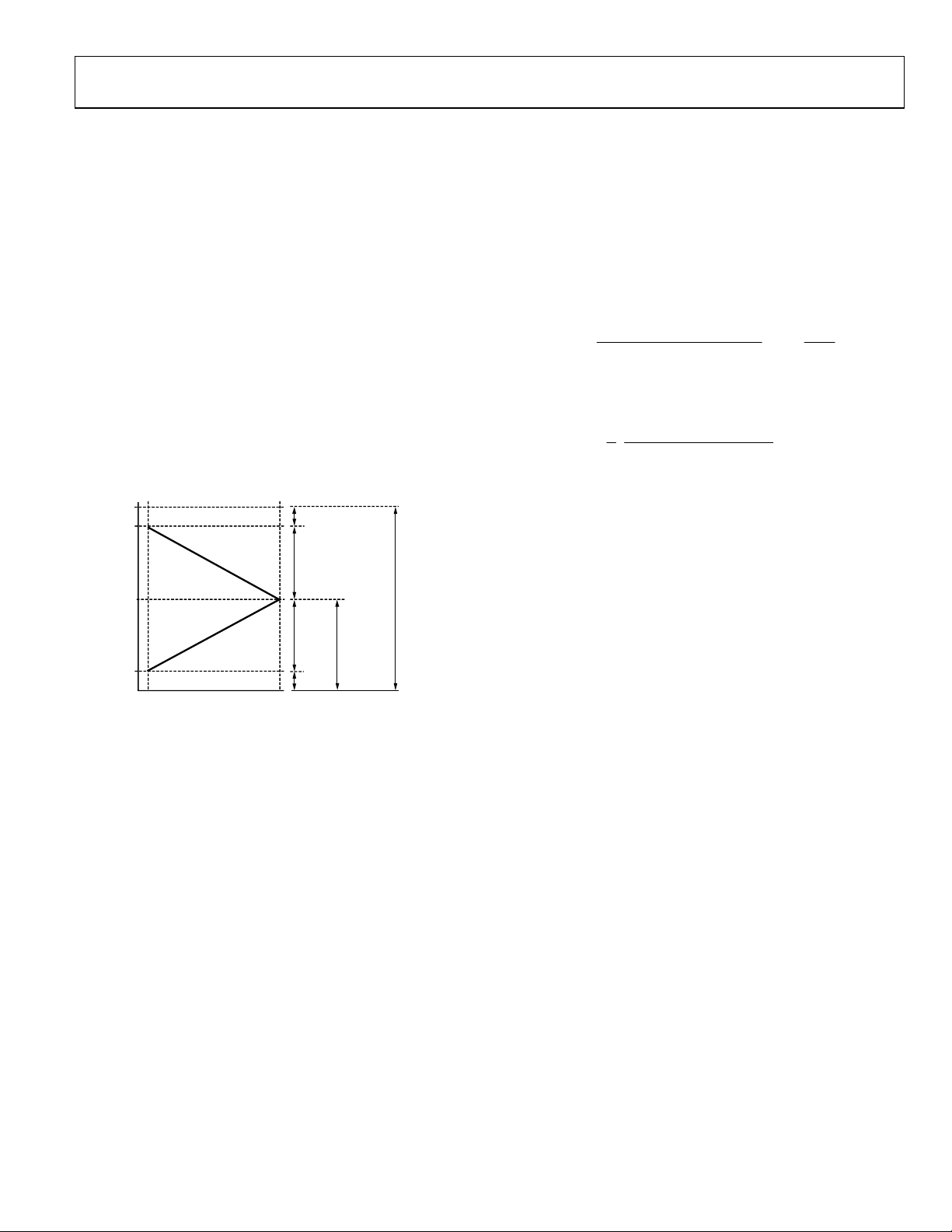
TRANSFER FUNCTION AND ANALOG OUTPUT VOLTAGE
The DecDriver has two regions of operation where the video
output voltages are either above or below the reference voltage
VRL. The transfer function defines the video output voltage as
the function of the digital input code as:
VOUTN(n) = VIDx(n) = VRL + VFS × (1 − n/4095),
for INV = HIGH
VOUTP(n) = VIDx(n) = VRL − VFS × (1 − n/4095),
for INV = LOW
ACCURACY
To best correlate transfer function errors to image artifacts, the
overall accuracy of the DecDriver is defined by three
parameters, VDE , VCME, and ΔVDE.
VDE, the differential error voltage, measures the difference
between the rms value of a channel and the ideal rms value of
that channel. The defining expression is
⎡⎤
VOUTN(n) VOUTP( n)
⎣⎦
VDE(n) 1 VFS
=−−
−
2409
n
⎛⎞
⎜⎟
⎝⎠
×
5
where n is the input code.
VFS = 2 × (VRH − VRL)
A number of internal limits define the usable range of the video
output voltages, VIDx, as shown in
VIDx – VOLTS
AVCC
(VRL + VFS)
VOUTN
VRL
VOUTP
(VRL – VFS)
AGND
0
INPUT CODE
VIDx vs. INPUT CODE
Figure 17. AD8387 Transfer Function and Usable Voltage Ranges
Figure 17.
≥1.3V
0 ≤ VFS ≤ 5.25V
0 ≤ VFS
5.25V ≤ VRL
≤ 5.25V
≤ (AVCC – 4)
≥1.3V
4095
INTERNAL LIMITS AND
USABLE VOLTAGE RANGES
11V ≤ AVCC
≤ 18V
VCME, the common-mode error voltage, measures ½ the dc
bias of a channel. The defining expression is
⎡
1
= VRL
nVCME
)(
⎢
2
⎣
+
2
nVOUTPnVOUTN
)()(
⎤
−
⎥
⎦
ΔVDE measures the maximum VDE mismatch between
channels. The defining equation is
ΔVDE = max{VDE(n)
} − min{VDE(n)
(0 − 11)
(0 − 11)
}
ΔV measures the maximum mismatch between channels. The
defining expression is
ΔV(n) = max{ΔVN(n), ΔVP(n)}
where:
ΔVN(n) = max{VOUTN(n)
ΔVP(n) = max{VOUTP(n)
05653-011
} − min{VOUTN(n)
(0 − 11)
} − min{VOUTP(n)
(0 − 11)
(0 − 11)
(0 − 11)
}
}
Rev. 0 | Page 13 of 16
Page 14

AD8387
APPLICATIONS
OPTIMIZED RELIABILITY WITH THE THERMAL SWITCH
While internal current limiters provide short-term protection
against temporary shorts at the outputs, the thermal switch
provides protection against persistent shorts lasting for several
seconds. To optimize reliability with the use of the thermal
switch, the following sequence of operations is recommended.
POWER-OFF SEQUENCE
1. Tur n o f f i n p ut s ig n al s
Tur n o f f V R L
2.
Tur n o f f V R H
3.
Turn off AVCC
4.
Tur n o f f DVC C
5.
INITIAL POWER-UP AFTER ASSEMBLY OR REPAIR
Grounded output mode is disabled, and thermal switch is
enabled. Ensure that the GSW pin is HIGH and that the
TSW pin is HIGH upon initial power-up and that they remain
unchanged throughout this procedure.
The initial power-up sequence follows:
1.
Execute the initial power-up.
2.
Identify any shorts at outputs. Power down, repair shorts,
and repeat the initial power-up sequence until proper system
functionality is verified.
Disable the thermal switch.
3.
POWER-UP DURING NORMAL OPERATION
Grounded output mode is disabled, and thermal switch is
disabled.
If TSW = LOW and GSW = HIGH, all outputs go into normal
operating mode with the thermal switch disabled.
POWER SUPPLY SEQUENCING
As indicated under the Absolute Maximum Ratings, the voltage
at any input pin cannot exceed its supply voltage by more than
0.5 V. Power-on and power-off sequencing can be required to
comply with the absolute maximum ratings.
Failure to comply with the Absolute Maximum Ratings can
result in functional failure or damage to the internal ESD
diodes. Damaged ESD diodes can cause temporary parametric
failures, which can result in image artifacts. Damaged ESD
diodes cannot provide full ESD protection, reducing reliability.
POWER-ON SEQUENCE
1. Turn on AVCC
Tur n o n VR H
2.
Tur n o n VR L
3.
Turn on DVCC
4.
Disable thermal switch: TSW = LOW
5.
6.
Turn on input signals
GROUNDED OUTPUT MODE DURING POWER-OFF
Certain applications require that video outputs be held near
AGND during power-down. The following power-off sequence
ensures that the outputs are near ground during power-off and
that the Absolute Maximum Ratings are not violated.
1.
Enable grounded output mode: GSW = LOW
Tur n o f f i n p ut s ig n al s
2.
3.
Tur n o f f V R L
Tur n o f f V R H
4.
Turn off AVCC
5.
Tur n o f f DVC C
6.
PCB DESIGN FOR OPTIMIZED THERMAL PERFORMANCE
Although the maximum safe operating junction temperature is
higher, the AD8387 is 100% tested at a junction temperature of
125°C. Consequently, the maximum guaranteed operating
junction temperature is 125°C. To limit the maximum junction
temperature at or below the guaranteed maximum, the package
in conjunction with the PCB must effectively conduct heat away
from the junction.
The AD8387 package is designed to provide enhanced thermal
characteristics through the exposed die paddle on the bottom
surface of the package. To take full advantage of this feature, the
exposed paddle must be in direct thermal contact with the PCB,
which then serves as a heat sink.
A thermally effective PCB must incorporate two thermal
pads and a thermal via structure. The thermal pad on the top
surface of the PCB provides a solderable contact surface on the
top surface of the PCB. The thermal pad on the bottom PCB
layer provides a surface in direct contact with the ambient. The
thermal via structure provides a thermal path to the inner and
bottom layers of the PCB to remove heat.
Rev. 0 | Page 14 of 16
Page 15

AD8387
THERMAL PAD DESIGN
To minimize thermal performance degradation of production
PCBs, the contact area between the thermal pad and the PCB
should be maximized. Therefore, the size of the thermal pad
on the top PCB layer should match the exposed paddle. The
second thermal pad of the same size should be placed on the
bottom side of the PCB. At least one thermal pad should be in
direct thermal contact with an external plane, such as AVCC
or GND.
THERMAL VIA STRUCTURE DESIGN
Effective heat transfer from the top to the inner and bottom
layers of the PCB requires thermal vias incorporated into the
thermal pad design. Thermal performance increases
logarithmically with the number of vias.
16mm
6.5mm
6.5mm
16mm
05653-012
Figure 18. Land Pattern—Top Layer
Near optimum thermal performance of production PCBs is
attained only when tightly spaced thermal vias are placed on
the full extent of the thermal pad.
Thermal Pad and Thermal via Connections
The thermal pad on the solder side is connected to a plane. The
use of thermal spokes is not recommended when connecting
the thermal pads or via structure to the plane.
Solder Masking
Solder masking of the via holes on the top layer of the PCB
plugs the via holes, inhibiting solder flow into the holes. To
minimize the formation of solder voids due to solder flowing
into the via holes (solder wicking), via diameter should be made
small, and an optional solder mask can be used. To optimize the
thermal pad coverage when using the solder mask, its diameter
should be no more than 0.1 mm larger than the via hole
diameter.
Pads are set by customer’s PCB design rules.
Thermal via Holes—Circular mask, centered on the via holes.
Diameter of the mask should be 0.1 mm larger than the via hole
diameter.
Solder Mask—Bottom Layer
This is set by customer’s PCB design rules.
6.5mm
6.5mm
Figure 19. Land Pattern—Bottom Layer
Figure 20. Solder Mask—Top Layer
05653-014
05653-013
AD8387 PCB DESIGN RECOMMENDATIONS
Table 5. Land Pattern Dimensions
Pad Size Pad Pitch Thermal Pad Size Thermal Via Structure
0.6 mm × 0.25 mm 0.5 mm 6 mm × 6 mm 0.25 mm − 0.35 mm holes
0.5 mm − 1.0 mm grid
Rev. 0 | Page 15 of 16
Page 16

AD8387
OUTLINE DIMENSIONS
14.20
0.75
0.60
0.45
1.20
MAX
14.00 SQ
13.80
1
PIN 1
12.20
12.00 SQ
11.80
6180
60
61 80
60
1
EXPOSED
PAD
BOTTOM VIEW
(PINS UP)
0.27
0.22
0.17
BSC SQ
20
21
1.05
1.00
0.95
0.15
0.05
SEATING
PLANE
0° MIN
0.08 MAX
COPLANARITY
0.20
0.09
3.5°
TOP VIEW
(PINS DOWN)
7°
0°
20
21
VIEW A
40 40
41
41
0.50 BSC
LEAD PITCH
VIEW A
ROTATED 90° CCW
COMPLIANT TO JEDEC STANDARDS MS-026-ADD-HD
Figure 21. 80-Lead Thin Quad Flat Package, Exposed Pad [TQFP_EP]
(SV-80-1)
Dimensions shown in millimeters
ORDERING GUIDE
Model Temperature Range Package Description Package Option
AD8387JSVZ
AD8387-EB Evaluation Board
1
Z = Pb-free part.
1
0°C to 85°C 80-Lead TQFP SV-80-1
6.00
© 2005 Analog Devices, Inc. All rights reserved. Trademarks and
registered trademarks are the property of their respective owners.
D05653-0-10/05(0)
Rev. 0 | Page 16 of 16
 Loading...