

Page 1
10-Bit, 12-Channel Output
FEATURES
High voltage drive
To within 1.3 V of supply rails
Output short-circuit protection
High update rates
Fast, 100 Ms/s 10-bit input data update rate
Static power dissipation: 1.4 W
Voltage-controlled video reference (brightness), offset,
and full-scale (contrast) output levels
INV bit reverses polarity of video signal
3.3 V logic, 9 V to 18 V analog supplies
High accuracy voltage outputs
Laser trimming eliminates the need for adjustments or
calibration
Flexible logic
XFR allows parallel AD8386 operation
Fast settling into capacitive loads
35 ns settling time to 0.25% into 150 pF load
Slew rate 400 V/μs
Available in 64-lead 9 mm × 9 mm LFCSP_VQ
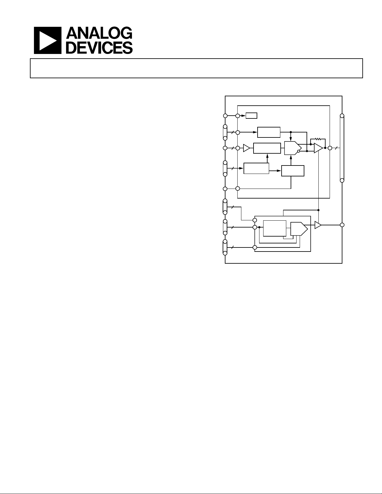
GENERAL DESCRIPTION
The AD8386 provides a fast, 10-bit, latched, decimating digital
input that drives 12 high voltage outputs. Input words with
10 bits are loaded sequentially into 12 separate high speed,
bipolar DACs. Flexible digital input format allows several
AD8386s to be used in parallel in high resolution displays.
The output signal can be adjusted for dc reference, signal
inversion, and contrast for maximum flexibility.
BYP
VRH
VRH
VRL
DB(0:9)
R/L
CLK
XFR
INV
GCTL
GSW
TSW
SDI
SCL
SEN
SVRH
SVRL
SVRL
Decimating LCD Driver
AD8386
FUNCTIONAL BLOCK DIAGRAM
BIAS
2
10
3
3
3
2
SCALING
CONTROL
TWO-STAGE
LATCH
SEQUENCE
CONTROL
12-BIT
SHIFT
REGISTER
Figure 1.
10-BIT
DACs
INV
CONTROL
8-BIT
DAC
AD8386
VID0
VID1
VID2
VID3
VID4
12
VID5
VID6
VID7
VID8
VID9
VID10
VID11
VAO
05687-001
The AD8386 is fabricated on ADI’s fast bipolar, 26 V XFHV
process, which provides fast input logic, bipolar DACs with
trimmed accuracy and fast settling, high voltage, precision
drive amplifiers on the same chip.
The AD8386 dissipates 1.4 W nominal static power.
The AD8386 is offered in a 64-lead 9 mm × 9 mm LFCSP_VQ
package and operates over the commercial temperature range of
0°C to 85°C.
Rev. 0
Information furnished by Analog Devices is believed to be accurate and reliable. However, no
responsibility is assumed by Anal og Devices for its use, nor for any infringements of patents or ot her
rights of third parties that may result from its use. Specifications subject to change without notice. No
license is granted by implication or otherwise under any patent or patent rights of Analog Devices.
Trademarks and registered trademarks are the property of their respective owners.
One Technology Way, P.O. Box 9106, Norwood, MA 02062-9106, U.S.A.
Tel: 781.329.4700 www.analog.com
Fax: 781.461.3113 © 2005 Analog Devices, Inc. All rights reserved.
Page 2

AD8386
TABLE OF CONTENTS
Features.............................................................................................. 1
Reference and Control Input Descriptions............................. 13
General Description ......................................................................... 1
Functional Block Diagram .............................................................. 1
Revision History ............................................................................... 2
Specifications..................................................................................... 3
DecDriver® Section ....................................................................... 3
Serial Interface Section ................................................................ 5
Absolute Maximum Ratings............................................................ 6
Maximum Power Dissipation ..................................................... 6
Overload Protection..................................................................... 6
Exposed Paddle............................................................................. 6
ESD Caution.................................................................................. 6
Operating Temperature Range ................................................... 7
Pin Configuration and Function Descriptions............................. 8
DecDriver Block Diagram and Timing........................................ 10
Serial Interface Block Diagram and Timing ............................... 12
Transfer Function and Analog Output Voltage...................... 13
Accuracy...................................................................................... 14
3-Wire Serial Interface............................................................... 14
Output Operating Modes.......................................................... 14
Overload Protection................................................................... 14
Applications..................................................................................... 15
Optimized Reliability with the Thermal Protection Circuit 15
Operation in High Ambient Temperature.............................. 15
Power Supply Sequencing ......................................................... 15
Grounded Output Mode During Power-Off.......................... 15
Typical Application Circuits ..................................................... 16
PCB Design for Optimized Thermal Performance ............... 17
AD8386 PCB Design Recommendations ............................... 17
Outline Dimensions....................................................................... 19
Ordering Guide .......................................................................... 19
Functional Description.................................................................. 13
REVISION HISTORY
8/05—Revision 0: Initial Version
Rev. 0 | Page 2 of 20
Page 3

AD8386
SPECIFICATIONS
DECDRIVER® SECTION
At 25°C, AVCC = 15.5 V, DVCC = 3.3 V, T
Table 1.
Parameter Conditions Min Typ Max Unit
VIDEO DC PERFORMANCE
1
VDE DAC Code 450 to 800 −7.5 +7.5 mV
VCME DAC Code 450 to 800 −3.5 +3.5 mV
VIDEO OUTPUT DYNAMIC PERFORMANCE T
Data Switching Slew Rate 20% to 80%, VO = 5 V step 400 V/μs
Invert Switching Slew Rate 20% to 80%, VO = 10 V step 560 V/μs
Data Switching Settling Time to 1% 24 35 ns
Data Switching Settling Time to 0.25% 35 50 ns
Invert Switching Settling Time to 1% 80 130 ns
Invert Switching Settling Time to 0.25% 250 500 ns
Invert Switching Overshoot 10 V Step 100 200 mV
CLK and Data Feedthrough
All-Hostile Crosstalk
2
3
Amplitude 50 mV p-p
Glitch Duration 30 ns
DAC Transition Glitch Energy DAC code 511 to 512 0.6 nV-s
VIDEO OUTPUT CHARACTERISTICS
Output Voltage Swing AVCC − VOH, VOL − AGND 1.1 1.3 V
Output Voltage—Grounded Mode 200 mV
Data Switching Delay: t
INV Switching Delay: t
4
9
5
10
Output Current 100 mA
Output Resistance 29 Ω
REFERENCE INPUTS
VRL Range VRH ≥ VRL 5.25 AVCC − 4 V
VRH Range VRH ≥ VRL VRL AVCC V
VRH – VRL Range VFS = 2 × (VRH − VRL) 0 2.75 V
VRH Input Resistance To VRL 20 kΩ
VRL Input Current −45 μA
VRH Input Current 125 μA
RESOLUTION
Coding Binary 10 Bits
DIGITAL INPUT CHARACTERISTICS
CIN 3 pF
IIH 0.05 μA
IIL −2 μA
VIH 2 V
VIL 0.8 V
VTH 1.65 V
IIH TSW 330 μA
IIL TSW −2 μA
TSW R
10 kΩ
PULLDOWN
A MIN
= 0°C, T
= 85°C, VRH = 9.5 V, VRL = 7 V, unless otherwise noted.
A MAX
T
A MIN
A MIN
to T
to T
A MAX
, CL = 150 pF
A MAX
15 mV p-p
5 V step 12 14 16 ns
10 V step 15 17 19 ns
Rev. 0 | Page 3 of 20
Page 4

AD8386
Parameter Conditions Min Typ Max Unit
DIGITAL TIMING CHARACTERISTICS T
Maximum Input Data Update Rate 100 Ms/s
Data Setup Time: t1 1 ns
XFR Setup Time: t3 0 ns
INV Setup Time: t11 0 ns
Data Hold Time: t2 3.5 ns
XFR Hold Time: t4 4.5 ns
INV Hold Time: t12 4 ns
CLK High Time: t7 6 ns
CLK Low Time: t8 4 ns
1
VDE = differential error voltage. VCME = common-mode error voltage. Full-scale output voltage = VFS = 2 × (VRH − VRL). See the Accuracy section.
2
Measured on two outputs differentially as CLK and DB (0:9) are driven and XFR is held low.
3
Measured on two outputs differentially as the others are transitioning by 5 V. Measured for both states of INV.
4
Measured from 50% of rising CLK edge to 50% of output change. Measurement is made for both states of INV.
5
Measured from 50% of rising CLK edge, which follows a valid XFR, to 50% of output change. See Figure 6 for the definition.
A MIN
to T
A MAX
Rev. 0 | Page 4 of 20
Page 5

AD8386
SERIAL INTERFACE SECTION
At 25°C, AVCC = 15.5 V, DVCC = 3.3 V, T
Table 2.
Parameter Conditions Min Typ Max Unit
SERIAL DAC DC PERFORMANCE
DNL SVFS = 5 V −1 +1 LSB
INL SVFS = 5 V −1.5 +1.5 LSB
Output Offset Error −2.0 +2.0 LSB
Scale Factor Error −3.0 +3.0 LSB
SERIAL DAC OUTPUT DYNAMIC PERFORMANCE To 0.5%
VAO Settling Time, t26 C
VAO Settling Time, t26 C
SERIAL DAC OUTPUT CHARACTERISTICS
VAO Maximum SVRH − 1 LSB V
VAO Minimum SVRL V
VAO − Grounded Mode 150 mV
VAO Output Resistance All supplies OFF 75 kΩ
I
±30 mA
OUT
C
Low Range
LOAD
C
High Range
LOAD
REFERENCE INPUTS
SVRH Range SVRL < SVRH SVRL + 1 AVCC − 3.5 V
SVRL Range SVRL < SVRH AGND + 1.5 SVRH − 1 V
SVFS Range 1 8 V
SVRH Input Current SVRS = 5 V 0.1 μA
SVRL Input Current SVRS = 5 V −1.6 −1.3 mA
DIGITAL INPUT CHARACTERISTICS
CIN 3 pF
IIH 0.05 μA
IIL −1 μA
VIH 2.0 DVCC V
VIL DGND 0.8 V
VTH 1.65 V
DIGITAL TIMING CHARACTERISTICS T
SEN to SCL Setup Time, t20 10 ns
SCL, High Level Pulse Width, t21 10 ns
SCL, Low Level Pulse Width, t22 10 ns
SCL to SEN Hold Time, t23 10 ns
SDI Setup Time, t24 10 ns
SDI Hold Time, t25 10 ns
POWER SUPPLIES
DVCC, Operating Range 3 3.3 3.6 V
DVCC, Quiescent Current 54 75 mA
AVCC Operating Range 9 18 V
Total AVCC Quiescent Current 80 100 mA
OPERATING TEMPERATURES
Ambient Temperature Range, T
Ambient Temperature Range, T
1
Output VAO is designed to drive capacitive loads less than 0.002 μF or more than 0.047 μF. Load capacitances in the range 0.002 μF − 0.047 μF cause the output
overshoot to exceed 100 mV.
2
Operation at high ambient temperature requires a thermally optimized PCB layout (see the Applications section). In systems with limited or no airflow, the maximum
ambient operating temperature is limited to 70°C with the thermal protection enabled, VFS = 4 V, data update rate = 85 Ms/s. Operation at 85°C ambient temperature
requires the thermal protection circuit turned disabled (TSW = LOW).
1
1
2
A
2
A
A MIN
= 0°C, T
= 85°C, VRH = 9.5 V, VRL = 7 V, unless otherwise noted.
A MAX
= 100 pF 1 2 μs
L
= 33 μF 15 ms
L
0.002 μF
0.047 μF
to T
A MIN
A MAX
Still air, TSW = HIGH 0 70 °C
Still air, TSW = LOW 0 85 °C
Rev. 0 | Page 5 of 20
Page 6
AD8386
ABSOLUTE MAXIMUM RATINGS
Table 3.
Parameter Rating
Supply Voltage
AVCCx − AGNDx 18 V
DVCC − DGND 4.5 V
Input Voltage
Maximum Digital Input Voltage DVCC + 0.5 V
Minimum Digital Input Voltage DGND − 0.5 V
Maximum Analog Input Voltage AVCC + 0.5 V
Minimum Analog Input Voltage AGND − 0.5 V
Internal Power Dissipation
LFCSP @ TA = 25°C 3.7 W
Operating Temperature Range 0°C to 85°C
Storage Temperature Range –65°C to +125°C
Lead Temperature Range
(Soldering 10 sec)
1
300°C
Stresses above those listed under Absolute Maximum Ratings
may cause permanent damage to the device. This is a stress
rating only and functional operation of the device at these or
any other conditions above those indicated in the operational
section of this specification is not implied. Exposure to absolute
maximum rating conditions for extended periods may affect
device reliability.
1
64-lead VQ_LFCSP:
θJA = 27°C/W in still air (JEDEC STD, 4-layer PCB with 16 vias on Epad)
θJA = 25°C/W @ 200 lfm airflow (JEDEC STD, 4-layer PCB with 16 vias on Epad)
θJA = 24°C/W @ 400 lfm airflow (JEDEC STD, 4-layer PCB with 16 vias on Epad)
ΨJT = 0.2°C/W in still air (JEDEC STD, 4-layer PCB with 16 vias on Epad)
ΨJB = 13.8°C/W in still air (JEDEC STD, 4-layer PCB with 16 vias on Epad)
MAXIMUM POWER DISSIPATION
The maximum power that can be safely dissipated by the
AD8386 is limited by its junction temperature. The maximum
safe junction temperature for plastic encapsulated devices, as
determined by the glass transition temperature of the plastic, is
approximately 150°C. Exceeding this limit temporarily may
cause a shift in the parametric performance due to a change in
the stresses exerted on the die by the package. Exceeding a
junction temperature of 175°C for an extended period can
result in device failure.
OVERLOAD PROTECTION
The AD8386 overload protection circuit consists of an output
current limiter and a thermal protection circuit.
When TSW is LOW, the thermal protection circuit is disabled,
and the output current limiter is turned on. The maximum
current at any one output of the AD8386 is internally limited to
100 mA average. In the event of a momentary short circuit
between a video output and a power supply rail (AVCC or
AGND), the output current limit is sufficiently low to provide
temporary protection.
When TSW is HIGH, the output current limiter, as well as the
thermal protection circuit, is turned on. The thermal protection
circuit debiases the output amplifier when the junction
temperature reaches the internally set trip point. In the event of
an extended short circuit between a video output and a power
supply rail, the output amplifier current continues to switch
between 0 mA and 100 mA typical with a period determined by
the thermal time constant and the hysteresis of the thermal trip
point. The thermal protection circuit limits the average junction
temperature to a safe level, which provides long-term
protection.
EXPOSED PADDLE
To ensure optimal thermal performance, the exposed paddle
must be electrically connected to an external plane, such as
AVCC or GND, as described in the
Applications section.
ESD CAUTION
ESD (electrostatic discharge) sensitive device. Electrostatic charges as high as 4000 V readily accumulate
on the human body and test equipment and can discharge without detection. Although this product features
proprietary ESD protection circuitry, permanent damage may occur on devices subjected to high energy
electrostatic discharges. Therefore, proper ESD precautions are recommended to avoid performance
degradation or loss of functionality.
Rev. 0 | Page 6 of 20
Page 7

AD8386
(
)
OPERATING TEMPERATURE RANGE
The maximum operating junction temperature is 150°C. The
junction temperature trip point of the thermal protection
circuit is 165°C. Production tests guarantee a minimum
junction temperature trip point of 125°C.
Consequently, the maximum guaranteed operating junction
temperature is 125°C when the thermal protection circuit is
enabled and 150°C when the thermal protection circuit is
disabled.
To ensure operation within the specified operating temperature
range, it is necessary to limit the maximum power dissipation as
TT
−
P
DMAX
≈
AirStillJA
09.0 lfminAirflow
AJMAX
()
×−θ
59.0
3.00
STILL AIR
200LFM
400LFM
OVERLOAD
PROTECTION
ENABLED
DISABLED
2.75
2.50
2.25
2.00
720p HDTV
1.75
1.50
QUIESCENT
MAXIMUM POWER DISSIPATION (W)
1.25
1.00
40 45 50 55 60 65 70 75 80 9085 95
65 70 75 80 85 90 95 100 105 115110 120
Figure 2. Maximum Power Dissipation vs. Temperature
AMBIENT TEMPERATURE (°C)
The AD8386 is on a 4-layer JEDEC PCB with a thermally
optimized landing pattern with 16 vias.
The quiescent power dissipation of the AD8386 is 1.4 W.
05687-002
When driving a 12-channel 720p HDTV panel with an input
capacitance of 150 pF, the AD8386 dissipates 1.66 W when
displaying 1 pixel wide alternating white and black vertical lines
generated by a standard 720p HDTV input video.
Conditions include the following:
• AVCC = 15.5 V
• DVCC = 3.3 V
• VFS = 5 V
• C
= 150 pF
L
• f
= 74.25 MHz
PIXEL
• Black-to-white transition = 4 V
• Active video time = 75%
Figure 2 shows these power dissipations.
Rev. 0 | Page 7 of 20
Page 8

AD8386
PIN CONFIGURATION AND FUNCTION DESCRIPTIONS
DVCC
DGND
CLK
XFR
INV
R/L
TSTA
AGNDD
AVCCD
VRH
VRH
VRL
AGND0
VID0
AVCC0, 1
VID1
646362616059585756555453525150
49
NC
1
NC
2
DB0
3
DB1
4
DB2
5
DB3
6
DB4
7
DB5
8
DB6
9
DB7
10
DB8
11
DB9
12
SDI
13
SEN
14
SCL
15
GCTL
16
NC = NO CONNECT
PIN 1
INDICATOR
AD8386
TOP VIEW
(Not to Scale)
171819202122232425262728293031
BYP
TSW
GSW
DVCC
DGND
AGNDS
SVRL
SVRL
VAO
SVRH
AVCCS
AGND11
Figure 3. 64-Lead LFCSP_VQ Pin Configuration
VID11
VID10
AVCC10, 11
32
AGND9, 10
48
AGND1, 2
47
VID2
46
AVCC2, 3
45
VID3
44
AGND3, 4
43
VID4
42
AVCC4, 5
41
VID5
40
AGND5, 6
39
VID6
38
AVCC6, 7
37
VID7
36
AGND7, 8
35
VID8
34
AVCC8, 9
33
VID9
05687-003
Rev. 0 | Page 8 of 20
Page 9

AD8386
Table 4. 64-Lead LFCSP_VQ Pin Function Descriptions
Pin No. Mnemonic Function Description
1, 2 NC No Connect No Internal Connection.
3 to 12 DB0 to DB9 Data Input 10-Bit Data Input. MSB = DB(9).
13 SDI Serial Data Input
14 SEN Serial DAC Enable
15 SCL Serial Data Clock Serial Data Clock.
16 GCTL Output Mode Control
17 GSW Output Mode Switch
18 TSW Thermal Switch
19, 64 DVCC Digital Power Supply Digital Power Supply.
20, 63 DGND Digital Ground Digital Supply Return.
21 AGNDS Analog Ground Analog Supply Return.
22, 23, 24 SVRL, SVRH Serial DAC Reference Voltage The voltage applied between these pins sets the serial DAC full-scale voltage.
25 VAO Serial DAC Output This output voltage is updated in the rising edge of the SEN input.
26 AVCCS Analog Power Supply Analog Power Supply.
27 BYP Bypass
28, 32, 36,
40, 44, 48, 52
29, 31, 33, 35,
37, 39, 41, 43,
45, 47, 49, 51
30, 34, 38,
42, 46, 50
53 VRL Video Center Reference
54, 55 VRH Full-Scale Reference The full-scale video output voltage is VFS = 2 × (VRH − VRL).
56 AVCCD Analog Power Supply Analog Power Supply.
57 AGNDD Analog Ground Analog Supply Return.
58 TSTA Test Pin Connect this pin to AGND.
59 R/L Right/Left Select
60 INV Invert
61 XFR Transfer/Start Sequence
62 CLK Clock Video Data Clock.
AGND11 to
AGND0
VID11 to
VID0
AVCC10, 11
to AVCC0, 1
Analog Ground Analog Supply Returns.
Analog Output These pins are directly connected to the analog inputs of the LCD panel.
Analog Power Supply Analog Power Supplies.
While the SEN input is LOW, one 12-bit serial word is loaded into the
serial DAC on the rising edges of the SCL.
A falling edge of this input initiates a loading cycle. While this input is held
LOW, the serial DAC is enabled and data is loaded on every rising edge of
SCL. The output is updated on the rising edge of a valid SEN. A valid
SEN must remain LOW for at least three SCL cycles. While this input is
held HIGH, the control DAC is disabled.
When this input is HIGH, the output mode is determined by the function
programmed into the serial interface. When LOW, the output mode is
controlled by the GSW input.
When GCTL is LOW and this input is HIGH, the video outputs and VAO
operate normally. When GCTL and this input are both LOW, the video
outputs and VAO are asynchronously forced to AGND, regardless of
the function programmed into the serial interface. This function operates
when AVCC power is OFF but requires DVCC power supply to be ON.
When this input is LOW, the thermal protection circuit is disabled. When
HIGH, the thermal protection circuit is enabled. This pin has a 10 kΩ
internal pull-down resistor.
A 0.1 μF capacitor connected between this pin and AGND ensures
optimum settling time.
The voltage applied to this pin sets the video center voltage. The video
outputs are above this reference while the INV = HIGH and below this
reference while INV = LOW.
A new data loading sequence begins on the left with Channel 0 when
this input is LOW, and on the right with Channel 11 when this input is HIGH.
When this input is HIGH, the VIDx output voltages are above VRL. When
LOW, the VIDx outputs voltages are below VRL. The state of INV is latched
on the first rising CLK edge after XFR is detected. The VIDx outputs change
on the rising CLK edge after the next XFR is detected.
The state of XFR is detected on the rising edge of CLK. Data is transferred to
the outputs and a new loading sequence begins on the next rising edge of
CLK after XFR is detected HIGH.
Rev. 0 | Page 9 of 20
Page 10

AD8386
DECDRIVER BLOCK DIAGRAM AND TIMING
TWO-
BYP
DB(0:9)
CLK
XFR
R/L
INV
BIAS
10
SEQUENCE
CONTROL
INV
CONTROL
10
STAGE
LATCH
10
STAGE
LATCH
10
STAGE
LATCH
10
STAGE
LATCH
10
STAGE
LATCH
10
STAGE
LATCH
10
10
STAGE
LATCH
10
STAGE
LATCH
10
STAGE
LATCH
10
STAGE
LATCH
10
STAGE
LATCH
10
STAGE
LATCH
SCALING
CONTROL
TWO-
TWO-
TWO-
TWO-
TWO-
TWO-
TWO-
TWO-
TWO-
TWO-
TWO-
10
DAC
10
DAC
10
DAC
10
DAC
10
DAC
10
DAC
10
DAC
10
DAC
10
DAC
10
DAC
10
DAC
10
DAC
VID0
VID2
VID4
VID6
VID8
VID10
VID1
VID3
VID5
VID7
VID9
VID11
VRL
VRH
Figure 4. AD8386 DecDriver Section
Rev. 0 | Page 10 of 20
05687-004
Page 11

AD8386
CLK
DB(0:9)
XFR
INV
VID(0:11)
VRL + VFS
VRL
t
f
t
8
V
TH
t
1
t
2
V
TH
05687-005
CLK
DB(0:9)
XFR
t
r
t
7
t
1
t
3
t
2
V
t
4
TH
Figure 5. Input Timing
–9 –8 –7 –6 –5 –4 –3 –1 1 2 3 4 5 6 7 8 9 11 13 14 15
t
9
t
MIN
11
t
MAX
11
010
–2
50%
–12, –11, –10, –9, –8, –7, –6, –5, –4, –3, –2, –1
t
9
t
12
PIXELS
12
t
10
0, 1, 2, 3, 4, 5, 6, 7, 8, 9, 10, 11
VRL
VRL – VFS
PIXELS
05687-006
Figure 6. Output Timing (R/L LOW)
Table 5.
Parameter Conditions Min Typ Max Unit
Data Setup Time, t1 Input tr, tf = 2 ns 1 ns
Data Hold Time, t2 3.5 ns
XFR Setup Time, t3 0 ns
XFR Hold Time, t4 4.5 ns
CLK High Time, t7 6 ns
CLK Low Time, t8 4 ns
Data Switching Delay, t9 12 14 16 ns
Invert Switching Delay, t10 15 17 19 ns
Invert Setup Time, t11 0
Invert Hold Time, t12 4
ns
ns
Rev. 0 | Page 11 of 20
Page 12

AD8386
SERIAL INTERFACE BLOCK DIAGRAM AND TIMING
SVRH
SVRL
SDI
SCL
SEN
12-BIT SHIFT REGISTER
SDI
CODE
SD0 SD1 SD2 SD3 SD4 SD5 SD6 SD7 SD8 SD9 SD10 SD11
SDI
CODE
8
SELECT LOAD
VAO = SVRL + SDI
SDAC
CONTROL
× (SVRH – SVRL)/256
CODE
VAO
75kΩ
TSW
10kΩ
VIDEO
DACs
GSW
GCTL
SEN
SCL
SDI
D11 D10 D9 D8 D7 D6 D5 D4 D3 D2 D1 D0
VAO
Figure 8. Serial Interface Timing Diagram
THERMAL
SWITCH
12
Figure 7. Serial Interface Block Diagram
05687-008
SEN
SCL
SDI
VAO
12
12
D11
t
22
t
21
t25t
D10
D0
D1
t
20
24
Figure 9. Serial Interface Timing Diagram
t
23
VID(0:11)
t
26
05687-007
05687-009
Table 6.
Parameter Conditions Min Typ Max Unit
SEN to SCL Setup Time, t20 10 ns
SCL, High Level Pulse Width, t21 10 ns
SCL, Low Level Pulse Width, t22 10 ns
SCL to SEN Hold Time, t23 10 ns
SDI Setup Time, t24 10 ns
SDI Hold Time, t25 10 ns
VAO Settling Time, t26 SVFS = 5 V, to 0.5 %, CL = 100 pF 1 2 μs
VAO Settling Time, t26 SVFS = 5 V, to 0.5 %, CL = 33 μF 15 ms
Rev. 0 | Page 12 of 20
Page 13

AD8386
FUNCTIONAL DESCRIPTION
The AD8386 is a system building block designed to
directly drive the columns of LCD microdisplays of the type
popularized for use in projection systems. It has 12 channels of
precision, 10-bit digital-to-analog converters (DACs) loaded
from a single high speed serial input. Precision current feedback
amplifiers, which provide well-damped pulse response and fast
voltage settling into large capacitive loads, buffer the 12 outputs.
Laser trimming at the wafer level ensures low absolute output
errors and tight channel-to-channel matching. Tight part-topart matching in high resolution systems is guaranteed by the
use of external voltage references.
REFERENCE AND CONTROL INPUT DESCRIPTIONS
Data transfer/start sequence control—input data loading,
data transfer.
A valid XFR control input initiates a new six-clock loading
cycle, during which data is transferred to the outputs, and 12
input data-words are loaded sequentially into the 12 internal
channels. Data is loaded on both the rising and falling edges of
CLK. Data loaded from the previous cycle is transferred to the
outputs on the rising CLK edge when the XFR is held HIGH at
the preceding rising CLK edge only. A new loading sequence
begins on the current rising CLK edge when XFR is held HIGH
at the preceding rising CLK edge only.
An internal 10 kΩ pull-down resistor disables the thermal
switch when this pin is left unconnected.
GCTL, GSW controls—output mode control.
Table 7. GTCL, GSW Truth Table
GTCL GSW Action
0 0
All video outputs and VAO are forced near
AGND. While the outputs are disabled, AVCC can
be removed.
0 1 All video outputs and VAO operate normally.
1 X
Output operating mode is controlled by the
serial interface.
TRANSFER FUNCTION AND ANALOG OUTPUT VOLTAGE
The DecDriver has two regions of operation where the video
output voltages are either above or below the reference voltage
VRL. The transfer function defines the video output voltage as
the function of the digital input code as
VIDx(n) = VRL + VFS × (1 − n/1023), for INV = HIGH
VIDx(n) = VRL − VFS × (1 − n/1023), for INV = LOW
where:
n = input code
Right/left control—input data loading.
To facilitate image mirroring, the direction of the loading
sequence is set by the R/L control.
A new loading sequence begins at Channel 0 and proceeds to
Channel 11 when the R/L control is held LOW. It begins at
Channel 11 and proceeds to Channel 0 when the R/L control is
held HIGH.
VRH, VRL inputs—full-scale video reference inputs.
The full-scale output voltage is VFS = 2 × (VRH − VRL).
INV control—analog output inversion.
The analog voltage equivalent of the input code is subtracted
from (VRL + VFS) while INV is held HIGH, and added to
(VRL − VFS) while INV is held LOW.
The state of the INV input is latched on the first rising edge of
CLK, immediately following a valid XFR. The VIDx outputs
invert on the first rising CLK edge, immediately following the
next valid XFR.
TSW control—thermal switch control.
VFS = 2 × (VRH − VRL)
A number of internal limits define the usable range of the video
output voltages, VIDx, shown in
VIDx – VOLTS
AVCC
(VRL + VFS)
VOUTN(n)
INV = HIGH
VRL
INV = LOW
VOUTP(n)
(VRL – VFS)
AGND
0
INPUT CODE (n)
VIDx vs. INPUT CODE
Figure 10. Transfer Function and Usable Voltage Ranges
Figure 10.
≥1.3V
0 ≤ VFS ≤ 5.5V
0 ≤ VFS
5.25V ≤ VRL
≤ 5.5V
≤ (AVCC – 4)
≥1.3V
1023
INTERNAL LIMITS AND
USABLE VOLTAGE RANGES
9V ≤ AVCC
≤ 18V
05687-010
When this input is HIGH, the thermal protection circuit is
enabled. When LOW or left unconnected, the thermal
protection circuit is disabled.
Rev. 0 | Page 13 of 20
Page 14

AD8386
()(
)
ACCURACY
To best correlate transfer function errors to image artifacts, the
overall accuracy of the DecDriver is defined by two parameters,
VDE and VCME.
VDE, the differential error voltage, measures the difference
between the rms value of the output and the rms value of the
ideal. The defining expression is
[]
()
=
nVDE ×
−
2
nnVOUTPnVOUTN
⎛
1
⎜
⎝
−−
1023
⎞
VFS
⎟
⎠
VCME, the common-mode error voltage, measures ½ the dc
offset of the output. The defining expression is
() ()
1
⎡
()
= VRL
nVCME
⎢
⎣
+
22
nVOUTPnVOUTN
⎤
−
⎥
⎦
3-WIRE SERIAL INTERFACE
The serial interface controls the 8-bit serial DAC and the video
output operating mode via a 12-bit serial word. The two most
significant bits (MSB) select the function and the eight least
significant bits (LSB) are the data for the serial DAC.
Table 8. Bit Definitions
Bit Name Bit Functionality
SD (0:7) 8-Bit SDAC Data. MSB = SD7.
SD8 Not Used.
SD9 Not Used.
SD10 VAO Load Selection.
SD11 Output Mode Selection When GCTL = 1.
Table 9. Truth Table @ GCTL = HIGH
SEN SD Action
11 10 9 8
0 0 X X Normal Output Mode. No change to VAO.
0 1 X X Normal Output Mode. Load VAO.
1 0 X X
1 1 X X Grounded Output Mode. Load VAO.
X X X X
Grounded Output Mode. No change to
VAO.
Start a Serial Interface Loading Cycle. No
change to VAO.
Table 10. Truth Table @ GCTL = LOW
SEN SD Action
11 10 9 8
X 0 XXNo Change to VAO.
X 1 XXLoad VAO.
X X X X
Start a Serial Interface Loading Cycle. No
change to VAO.
Serial DAC
The serial DAC is loaded via the serial interface. The output
voltage is determined by
VAO = SVRL + (SVRH − SVRL) × n/256
where n is the SD(0:7) serial input code.
Output VAO is designed to drive capacitive loads less than
0.002 μF or more than 0.047 μF. Load capacitances in the
0.002 μF − 0.047 μF range cause the output overshoot to exceed
100 mV.
OUTPUT OPERATING MODES
In normal operating mode, the voltage of the video outputs is
determined by the inputs.
In grounded output mode, the video outputs are forced to
(AGND + 0.2 V) typ.
OVERLOAD PROTECTION
The overload protection employs current limiters and a thermal
protection circuit to protect the video output pins against accidental
shorts between any video output pin and AVCC or AGND.
The junction temperature trip point of the thermal protection
circuit is 165°C. Production tests guarantee a minimum
junction temperature trip point of 125°C. Consequently, the
operating junction temperature should not rise above 125°C
when the thermal protection circuit is enabled.
For systems that operate at high internal ambient temperatures
and require large capacitive loads to be driven by the AD8386 at
high frequencies, junction temperatures above 125°C may be
required. In such systems, the thermal protection circuit should
either be disabled or a minimum airflow of 200 lfm must be
maintained.
Rev. 0 | Page 14 of 20
Page 15

AD8386
APPLICATIONS
OPTIMIZED RELIABILITY WITH THE THERMAL PROTECTION CIRCUIT
The AD8386 is designed for enhanced reliability through
features that provide protection against accidental shorts that
may occur during PCB assembly repair, such as solder bridging,
or during system assembly, such as a misaligned flat panel cable
in the connector.
While internal current limiters provide short-term protection
against temporary shorts at the outputs, the thermal shutdown
provides protection against persistent shorts lasting for several
seconds. To optimize reliability, the following sequence of
operations is recommended.
Initial Power-Up after PCB Assembly or Repair
Disable grounded output mode and enable thermal protection.
Ensure that the GCTL and GSW pins are LOW and the TSW
pin is HIGH upon initial power-up and remains unchanged
throughout this procedure.
Execute the initial power-up.
•
Identify any shorts at the outputs.
•
•
Power-down, repair shorts, and repeat the initial power-up
sequence until proper system functionality is verified.
Power-Up during Normal Operation
Disable grounded output mode and disable the thermal
protection circuit using either of the following two methods:
POWER SUPPLY SEQUENCING
As indicated in the Absolute Maximum Ratings section, the
voltage at any input pin cannot exceed its supply voltage by
more than 0.5 V. Power-on and power-off sequencing may be
required to comply with the Absolute Maximum Ratings.
Failure to comply with the Absolute Maximum Ratings may
result in functional failure or damage to the internal ESD
diodes. Damaged ESD diodes may cause temporary parametric
failures, which may result in image artifacts. Damaged ESD
diodes cannot provide full ESD protection, reducing reliability.
The following power supply sequencing ensures that the
Absolute Maximum Ratings are not violated.
Power-on sequence is:
Turn ON AVCC and analog reference voltages.
•
•
Turn ON DVCC and digital signals.
Power-off sequence is:
•
Turn OFF AVCC and analog reference voltages.
Turn OFF DVCC and digital signals.
•
GROUNDED OUTPUT MODE DURING POWER-OFF
Certain applications require that the video outputs be held near
AGND during power-down. The following power-off sequence
ensures that the outputs are near ground during power-off and
the Absolute Maximum Ratings are not violated.
•
GCTL = HIGH, TSW = HIGH and serial code
0XXXXXXXXXXX sent immediately following a power-up,
places all outputs into normal operating mode and disables
the thermal protection circuit.
TSW = LOW disables the thermal protection circuit.
•
GCTL = LOW and GSW = HIGH puts all outputs into
normal operating mode.
OPERATION IN HIGH AMBIENT TEMPERATURE
To extend the maximum operating junction temperature of the
AD8386 to 150°C, keep the thermal protection circuit disabled
(TSW = LOW) during normal operation.
Rev. 0 | Page 15 of 20
Enable grounded output mode in one of two ways:
•
GTCL = LOW and GSW = LOW, or GCTL = HIGH
and code 1XXXXXXXXXXX sent via the serial interface.
Turn OFF AVCC and analog reference voltages.
•
•
Turn OFF DVCC and digital signals.
Page 16

AD8386
TYPICAL APPLICATION CIRCUITS
12-CHANNEL
LCD
SEN
VID0
VID1
VID2
VID3
VID4
VID5
VID6
VID7
VID8
VID9
VID10
VID11
VAO
PIXEL
CLK
PROCESSOR
÷2
IMAGE
μP
DB(0:9)
CLK
R/L
XFR
INV
REFERENCES
DB(0:9)
CLK
R/L
XFR
INV
VRH
VRL
SVRH
SVRL
SDI
AD8386
SCL
Figure 11. 12-Channel System
CHANNEL 0
CHANNEL 1
CHANNEL 2
CHANNEL 3
CHANNEL 4
CHANNEL 5
CHANNEL 6
CHANNEL 7
CHANNEL 8
CHANNEL 9
CHANNEL 10
CHANNEL 11
05687-015
PIXEL
CLK
PROCESSOR
÷2
IMAGE
DB(0:9)
CLK
R/L
XFR
INV
DB(0:9)
INV
μP
DB(0:9)
CLK
R/L
XFR
INV
SCL
SDI
SEN
REFERENCES
SCL
SDI
SEN
CLK
R/L
XFR
DB(0:9)
INV
Figure 12. 24-Channel System
VRH
AD8386
VRH
AD8386
VRL
VRL
SVRH
SVRH
VID0
VID1
VID2
VID3
VID4
VID5
VID6
VID7
VID8
VID9
VID10
VID11
SVRL
VAO
VID0
SVRL
VID1
VID2
VID3
VID4
VID5
VID6
VID7
VID8
VID9
VID10
VID11
VAO
CHANNEL 0
CHANNEL 1
CHANNEL 2
CHANNEL 3
CHANNEL 4
CHANNEL 5
CHANNEL 6
CHANNEL 7
CHANNEL 8
CHANNEL 9
CHANNEL 10
CHANNEL 11
24-CHANNEL
LCD
CHANNEL 12
CHANNEL 13
CHANNEL 14
CHANNEL 15
CHANNEL 16
CHANNEL 17
CHANNEL 18
CHANNEL 19
CHANNEL 20
CHANNEL 21
CHANNEL 22
CHANNEL 23
05687-016
Rev. 0 | Page 16 of 20
Page 17

AD8386
PCB DESIGN FOR OPTIMIZED THERMAL PERFORMANCE
The total maximum power dissipated by the AD8386 is partly
load dependent. In a 12-channel, 60 Hz XGA system running at
a 65 MHz pixel rate, the total maximum power dissipated is
1.7 W, assuming a 15.5 V analog power supply, a 4 V white-toblack swing, and a 150 pF LCD input capacitance.
To limit the operating junction temperature at or below the
guaranteed maximum, the package in conjunction with the
PCB must effectively conduct heat away from the junction.
The AD8386 package is designed to provide enhanced thermal
characteristics through the exposed die paddle on the bottom
surface of the package. In order to take full advantage of this
feature, the exposed paddle must be in direct thermal contact
with the PCB, which then serves as a heat sink.
A thermally effective PCB must incorporate two thermal pads
and a thermal via structure. The thermal pad on the top PCB
layer provides a solderable contact surface on the top surface of
the PCB. The thermal pad on the bottom PCB layer provides a
surface in direct contact with the ambient air. The thermal via
structure provides a thermal path to the inner and bottom
layers of the PCB to remove heat.
Bottom PCB Layer
It is recommended that the bottom thermal pad be thermally
connected to a plane. The connection should be direct such that
the thermal pad becomes part of the plane.
The use of thermal spokes is not recommended when
connecting the thermal pads or via structure to a plane.
Solder Masking
To minimize the formation of solder voids due to solder flowing
into the via holes (solder wicking), the via diameter should be
small. Optional solder masking of the via holes on the top layer
of the PCB plug the via holes, inhibiting solder flow into the
holes. To optimize the thermal pad coverage, the solder mask
diameter should be no more than 0.1 mm larger than the via
hole diameter.
Pads are set by the customer’s PCB design rules, and thermal
vias are 0.25 mm diameter circular mask, centered on the vias.
Thermal Pad Design
To minimize thermal performance degradation of production
PCBs, the contact area between the thermal pad and the PCB
should be maximized. Therefore, the size of the thermal pad on
the top PCB layer should match the exposed paddle size. The
second thermal pad of at least the same size should be placed on
the bottom side of the PCB. At least one thermal pad should be
in direct thermal contact with a plane, such as AVCC or GND.
Thermal via Structure Design
Effective heat transfer from the top to the inner and bottom
layers of the PCB requires thermal vias incorporated into the
thermal pad design. Thermal performance increases
logarithmically with the number of vias.
Near optimum thermal performance of production PCBs is
attained when tightly spaced thermal vias are placed on the full
extent of the thermal pad only.
AD8386 PCB DESIGN RECOMMENDATIONS
Table 11. Top PCB Layer
Pad Size
Pad Pitch
Thermal Pad Size
Thermal via Structure
0.25 mm × 0.4 mm
0.5 mm
4.7 mm × 4.7 mm
0.25 mm diameter vias on a 0.5 mm grid
05687-011
Figure 13. Land Patter—Top PCB Layer
05687-012
Figure 14. Land Patter—Bottom PCB Layer
05687-013
Figure 15. Solder Mask—Top Layer
Rev. 0 | Page 17 of 20
Page 18

AD8386
0.05
SOLDER MASK
SWELL
0.5
0.4
0.5
9.00
9.00
4.7 SQ CU w/4.8 SQ SOLDER MASK
R 0.05 OPTIONAL FILLETS
VIA ARRAY ON 0.5 GRID
0.25 DRILL, 0.35 SOLDER MASK SWELL
0.25
OPTIONAL FILLETS
R 0.05
Figure 16. Suggested Land Pattern
Dimensions shown in millimeters
Rev. 0 | Page 18 of 20
05285-014
Page 19

AD8386
OUTLINE DIMENSIONS
1.00
0.85
0.80
12° MAX
SEATING
PLANE
BSC SQ
PIN 1
INDICATOR
9.00
0.60 MAX
TOP
VIEW
0.80 MAX
0.65 TYP
0.50 BSC
*
COMPLIANT TO JEDEC STANDARDS MO-220-VMMD
EXCEPT FOR EXPOSED PAD DIMENSION
8.75
BSC SQ
0.20 REF
0.45
0.40
0.35
0.05 MAX
0.02 NOM
49
48
33
32
0.60 MAX
Figure 17. 64-Lead Lead Frame Chip Scale Package [LFCSP_VQ]
9 mm × 9 mm Body, Very Thin Quad (CP-64-1)
Dimensions shown in millimeters
EXPOSED PAD
(BOTTOM VIEW)
7.50
REF
0.30
0.25
0.18
64
17
1
16
PIN 1
INDICATOR
*
4.85
4.70 SQ
4.55
ORDERING GUIDE
Model Temperature Range Package Description Package Option
AD8386JCPZ
1
Z = Pb-free part.
1
0°C to 85°C 64-Lead Lead Frame Chip Scale Package (LFCSP_VQ) CP-64-1
Rev. 0 | Page 19 of 20
Page 20

AD8386
NOTES
© 2005 Analog Devices, Inc. All rights reserved. Trademarks and
registered trademarks are the property of their respective owners.
D05687–0–8/05(0)
Rev. 0 | Page 20 of 20
 Loading...