

Page 1
10-Bit, 6-Channel Decimating
PRODUCT FEATURES
High accuracy, high resolution voltage outputs
10-bit input resolution
Laser trimmed outputs
Fast settling, high voltage drive
30 ns settling time to 0.25% into a 150 pF load
Slew rate 460 V/µs
Outputs to within 1.3 V of supply rails
High update rates
Fast, 100 Ms/s 10-bit input data update rate
Voltage controlled video reference (brightness), offset, and
full-scale (contrast) output levels
Flexible logic
STSQ/XFR allow parallel AD8384 operation
INV bit reverses polarity of video signal
Output short-circuit protection
3.3 V logic, 9 V to 18 V analog supplies
18 V level shifters for panel timing signals
Available in 80-lead 12 mm × 12 mm TQFP E-pad
APPLICATIONS
LCD analog column drivers
LCD DecDriver
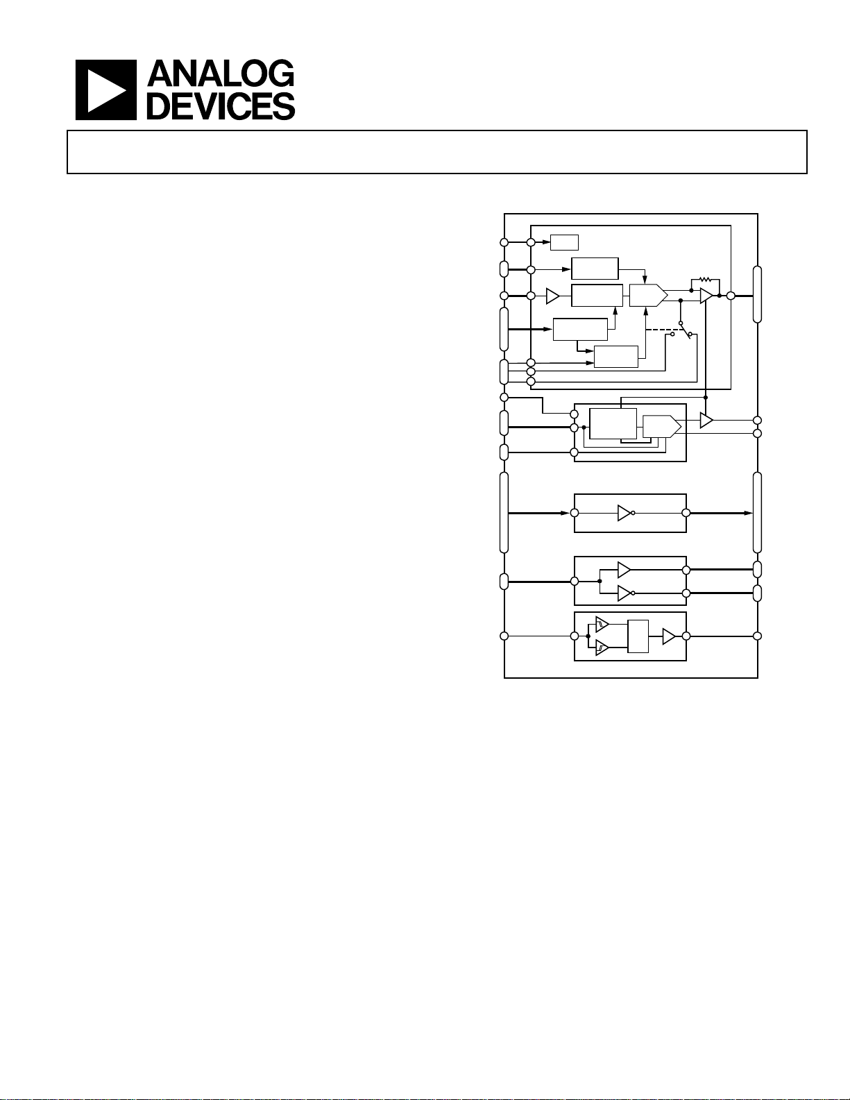
FUNCTIONAL BLOCK DIAGRAM
BYP
VRH
VRL
DB(0:9)
R/L
CLK
STSQ
XFR
INV
TSTM
SDI
SCL
SEN
SVRH
SVRL
DYIN
DXIN
DIRYIN
DIRXIN
NRGIN
ENBX1IN
ENBX2IN
ENBX3IN
ENBX4IN
CLXIN
CLYIN
10
V1
V2
BIAS
2
/
/
4
SEQUENCE
/
3
2
9
2
CONTROL
/
/
/
/
®
with Level Shifters
AD8384
SCALING
CONTROL
2-STAGE
LATCH
CONTROL
12-BIT
SHIFT
REGISTER
INV
DACs
DUAL
DAC
6
/
9
/
2
/
2
/
VID0
VID1
VID2
VID3
VID4
VID5
VAO1
VAO2
DY
DX
DIRY
DIRX
NRG
ENBX1
ENBX2
ENBX3
ENBX4
CLX
CLY
CLXN
CLYN
PRODUCT DESCRIPTION
The AD8384 DecDriver provides a fast, 10-bit, latched,
decimating digital input that drives six high voltage outputs.
10-bit input words are loaded sequentially into six separate high
speed, bipolar DACs. Flexible digital input format allows several
AD8384s to be used in parallel in high resolution displays. The
output signal can be adjusted for dc reference, signal inversion,
and contrast for maximum flexibility. Integrated level shifters
convert timing signals from a 3 V timing controller to high
voltage for LCD panel timing inputs. Two serial input, 8-bit
DACs are integrated to provide dc reference signals. DAC
addresses and 8-bit data are loaded in one 12-bit serial word.
Rev. 0
Information furnished by Analog Devices is believed to be accurate and reliable.
However, no responsibility is assumed by Analog Devices for its use, nor for any
infringements of patents or other rights of third parties that may result from its use.
Specifications subject to change without notice. No license is granted by implication
or otherwise under any patent or patent rights of Analog Devices. Trademarks and
registered trademarks are the property of their respective owners.
MONITI
R
S
AD8384
Figure 1.
The AD8384 is fabricated on the 26 V, fast, bipolar XFHV
process developed by Analog Devices, Inc. This process
provides fast input logic, bipolar DACs with trimmed accuracy
and fast settling, high voltage, precision drive amplifiers on the
same chip.
The AD8384 dissipates 1.1 W nominal static power.
The AD8384 is offered in an 80-lead 12 mm × 12 mm TQFP
E-pad package and operates over the 0°C to 85°C commercial
temperature range.
One Technology Way, P.O. Box 9106, Norwood, MA 02062-9106, U.S.A.
Tel: 781.329.4700
Fax: 781.326.8703 © 2004 Analog Devices, Inc. All rights reserved.
www.analog.com
MONITO
04512-0-001
Page 2

AD8384
TABLE OF CONTENTS
Specifications..................................................................................... 3
DecDriver...................................................................................... 3
Level Shifters ................................................................................. 5
Level Shifting Edge Detector ...................................................... 5
Serial Interface .............................................................................. 6
Power Supplies .............................................................................. 7
Operating Temperature ............................................................... 7
Absolute Maximum Ratings............................................................ 8
Maximum Power Dissipation ..................................................... 8
Operating Temperature Range ................................................... 8
Overload Protection ..................................................................... 8
Exposed Paddle............................................................................. 8
Pin Configuration and Function Descriptions............................. 9
Timing Characteristics................................................................... 11
DecDriver Section...................................................................... 11
Functional Description .................................................................. 15
Accuracy ...................................................................................... 16
TSTM Control—Test Mode ...................................................... 16
Grounded Output Mode ........................................................... 16
Overload Protection................................................................... 16
3-Wire Serial Interface............................................................... 16
Serial DACs................................................................................. 16
Level Shifters ............................................................................... 16
Applications..................................................................................... 17
Power Supply Sequencing ......................................................... 17
VBIAS Generation—V1, V2 Input Pin Functionality ........... 18
Applications Circuit ................................................................... 18
PCB Design for Optimized Thermal Performance ............... 19
Thermal Pad Design .................................................................. 19
Thermal Via Structure Design.................................................. 19
Level Shifter Section................................................................... 12
Level Shifting Edge Detector ....................................................13
Serial Interface ............................................................................ 14
REVISION HISTORY
Revision 0: Initial Version
AD8384 PCB Design Recommendations ............................... 20
Outline Dimensions....................................................................... 21
Ordering Guide .......................................................................... 21
Rev. 0 | Page 2 of 24
Page 3

AD8384
SPECIFICATIONS
DecDriver
Table 1. @ 25°C, AVCC = 15.5 V, DVCC = 3.3 V, T
unless otherwise noted
Parameter Conditions Min Typ Max Unit
VIDEO DC PERFORMANCE
1
T
VDE DAC Code 450 to 800 –7.5 +7.5 mV
VCME DAC Code 450 to 800 –3.5 +3.5 mV
VIDEO OUTPUT DYNAMIC PERFORMANCE T
Data Switching Slew Rate 20% to 80% 460 V/µs
Invert Switching Slew Rate 20% to 80% 560 V/µs
Data Switching Settling Time to 1% 19 24 ns
Data Switching Settling Time to 0.25% 30 50 ns
Invert Switching Settling Time to 1% VO = 10 V Step 75 120 ns
Invert Switching Settling Time to 0.25% VO = 10 V Step 250 500 ns
Invert Switching Overshoot VO = 10 V Step 100 200 mV
CLK and Data Feedthrough
All-Hostile Crosstalk
2
3
10 mV p-p
Amplitude 10 mV p-p
Glitch Duration 30 ns
DAC Transition Glitch Energy DAC Code 511 to 512 0.3 nV-s
VIDEO OUTPUT CHARACTERISTICS
Output Voltage Swing AVCC – VOH, VOL – AGND 1.1 1.3 V
Output Voltage—Grounded Mode 0.25 V
Data Switching Delay: t
INV Switching Delay: t
4
9
5
10
50 % of VIDx 10 12 14 ns
50 % of VIDx 13 15 17 ns
Output Current 100 mA
Output Resistance 22 Ω
REFERENCE INPUTS
V1 Range V2 ≥ (V1-0.25V) 5.25 AVCC – 4 V
V2 Range V2 ≥ (V1-0.25V) 5.25 AVCC – 4 V
V1 Input Current –3 µA
V2 Input Current –14 µA
VRL Range VRH ≥ VRL V1 – 0.5 AVCC – 1.3 V
VRH Range VRH ≥ VRL VRL AVCC V
(VRH–VRL) Range VFS = 2(VRH – VRL) 0 2.75 V
VRH Input Resistance To VRL 20 kΩ
VRL Bias Current –0.2 µA
VRH Input Current 125 µA
RESOLUTION
Coding Binary 10 Bits
1
VDE = differential error voltage; VCME = common-mode error voltage; VFS = full-scale output voltage = 2 × (VRH – VRL). See the section. Accuracy
2
Measured differentially on two outputs as CLK and DB(0:9) are driven and STSQ and XFR are held LOW.
3
Measured differentially on two outputs as the other four are transitioning by 5 V. Measured for both states of INV.
4
Measured from 50% of rising CLK edge to 50% of output change. Measurement is made for both states of INV.
5
Measured from 50% of rising CLK edge to 50% of output change. Refer to Figure 7 for the definition.
A MIN
A MIN
A MIN
to T
to T
= 0°C, T
A MAX
, VO = 5 V Step, CL = 150 pF
A MAX
= 85°C, VRH = 9.5 V, VRL = V1 = V2 = 7 V,
A MAX
Rev. 0 | Page 3 of 24
Page 4

AD8384
DecDriver (continued)
Parameter Conditions Min Typ Max Unit
DIGITAL INPUT CHARACTERISTICS
Max. Input Data Update Rate 100 Ms/s
CLK to Data Setup Time: t
CLK to STSQ Setup Time: t
CLK to XFR Setup Time: t
CLK to Data Hold Time: t
CLK to STSQ Hold Time: t
CLK to XFR Hold Time: t
CLK High Time: t
CLK Low Time: t
7
8
1
3
5
2
4
6
CIN 3 pF
I
IH
I
IL
V
IH
V
IL
V
TH
0 ns
0 ns
0 ns
3 ns
3 ns
3 ns
3 ns
2.5 ns
0.05 µA
–0.6 µA
2 V
0.8 V
1.65 V
Rev. 0 | Page 4 of 24
Page 5

AD8384
LEVEL SHIFTERS
Table 2. @ 25°C, AVCC = 15.5 V, DVCC = 3.3 V, T
unless otherwise noted
Parameter Conditions Min Typ Max Unit
LEVEL SHIFTER LOGIC INPUTS
CIN 3 pF
IIH 0.05 µA
IIL –0.6 µA
VTH 1.65 V
VIH 2.0 DVCC V
VIL DGND 0.8 V
LEVEL SHIFTER OUTPUTS RL ≥ 10 kΩ
VOH AVCC – 0.45 AVCC – 0.25 V
VOL 0.25 0.45 V
LEVEL SHIFTER DYNAMIC PERFORMANCE T
Output Rise, Fall Times—tr, tf
DX, CLX, CLXN, ENBX(1–4) CL = 40 pF 18.5 30 ns
DY, CLY, CLYN CL = 40 pF 40 70 ns
DIRX, DIRY CL = 40 pF 100 150 ns
NRG CL = 200 pF 35 50 ns
C
Propagation Delay Times—t11, t12, t13, t14
DX, CLX, CLXN, ENBX(1–4) CL = 40 pF 20 50 ns
DY, CLY, CLYN CL = 40 pF 29 50 ns
DIRX, DIRY CL = 40 pF 60 100 ns
NRG CL = 200 pF 25 55 ns
C
Output Skew
ENBX(1–4)—t15, t16 C
DX to ENBX(1–4)—t16 C
DX to CLX—t15, t16, t17, t18 C
DY to CLY, CLYN—t15, t16, t17, t18 C
A MIN
= 0°C, T
A MIN
L
L
L
L
L
L
= 85°C, VRH = 9.5 V, VRL = V1 = V2 = 7 V,
A MAX
to T
A MAX
= 300 pF 55 100 ns
= 300 pF 32 ns
= 40 pF 2 ns
= 40 pF 2 ns
= 40 pF 10 ns
= 40 pF 20 ns
LEVEL SHIFTING EDGE DETECTOR
Table 3. CL = 10 pF, T
Parameter Min Typ Max Unit
VIL Input Low Voltage AGND AGND + 2.75 V
VIH Input High Voltage AVCC – 2.7 AVCC V
VTH LH Input Rising Edge Threshold Voltage AGND + 3 V
VTH HL Input Falling Edge Threshold Voltage AVCC – 3 V
VOH Output High Voltage DVCC – 0.45 DVCC – 0.25 V
VOL Output Low Voltage 0.25 0.45 V
IIH Input Current High State 1.2 2.5 µA
IIL Input Current Low State –2.5 –1.2 µA
t19 Input Rising Edge Propagation Delay Time 16 ns
∆t19 t
19
t20 Input Falling Edge Propagation Delay Time 12 ns
∆t20 t
20
tr Output Rise Time 5 ns
tf Output Fall Time 6 ns
A MIN
to T
, unless otherwise noted
A MAX
Variation with Temperature 2 ns
Variation with Temperature 2 ns
Rev. 0 | Page 5 of 24
Page 6

AD8384
SERIAL INTERFACE
Table 4. @ 25°C, AVCC = 15.5 V, DVCC = 3.3 V, T
Parameter Conditions Min Typ Max Unit
SERIAL DAC REFERENCE INPUTS SVFS = (SVRH – SVRL)
SVRH Range SVRL < SVRH SVRL + 1 AVCC – 3.5 V
SVRL Range SVRL < SVRH AGND + 1.5 SVRH – 1 V
SVFS Range 1 8 V
SVRH Input Current SVFS = 5 V –70 nA
SVRL Input Current SVFS = 5 V –2.8 –2.5 mA
SVRH Input Resistance 40 kΩ
SERIAL DAC ACCURACY
DNL SVFS = 5 V, RL = ∞ –1.0 +1.0 LSB
INL SVFS=5 V, RL = ∞ –1.5 +1.5 LSB
Output Offset Error –2.0 +2.0 LSB
Scale Factor Error –4.0 +4.0 LSB
SERIAL DAC LOGIC INPUTS
C
IN
3 pF
IIL –0.6 µA
I
IH
0.05 µA
VTH 1.65 V
VIH 2.0 DVCC V
VIL DGND 0.8 V
SERIAL DAC OUTPUTS
Maximum Output Voltage SVRH – 1 LSB V
Minimum Output Voltage SVRL V
VAO1—Grounded Mode 0.1 V
I
OUT
C
Low Range
LOAD
C
High Range1 0.047 µF
LOAD
6
±30 mA
0.002 µF
SERIAL DAC DYNAMIC PERFORMANCE
SEN to SCL Setup Time, t
20
SCL, High Level Pulse Width, t
SCL, Low Level Pulse Width, t
SDI Setup Time, t
SDI Hold Time, t
SCL to SEN Hold Time, t
24
25
23
VAO1, VAO2 Settling Time, t
VAO1, VAO2 Settling Time, t
21
22
26
26
10 ns
15 ns
10 ns
10 ns
10 ns
15 ns
SVFS = 5 V, to 0.5%, CL = 100 pF 1 2 µs
SVFS = 5 V, to 0.5%, CL = 33 µF 10 15 ms
6
Outputs VAO1 and VAO2 are designed to drive very high capacitive loads. The load capacitance must be ≤ 0.002 µF or ≥0.047 µF.
Load capacitance in the range 0.002 µF to 0.047 µF causes the output overshoot to exceed 100 mV.
A MIN
= 0°C, T
= 85°C, SVRL = 4 V, SVRH = 9 V, unless otherwise noted
A MAX
Rev. 0 | Page 6 of 24
Page 7
AD8384
POWER SUPPLIES
Table 5. @ 25°C, AVCC = 15.5 V, DVCC = 3.3 V, T
Parameter Min Typ Max Unit
DVCC, Operating Range 3 3.3 3.6 V
DVCC, Quiescent Current 40 50 mA
AVCC Operating Range 9 18 V
Total AVCC Quiescent Current 70 85 mA
OPERATING TEMPERATURE
Parameter Conditions Min Typ Max Unit
Ambient Temperature Range, T
Ambient Temperature Range, T
Junction Temperature Range, TJ 100% Tested 25 125 °C
7
Operation at high ambient temperature requires a thermally optimized PCB layout (see the Applications section), input data update rate not exceeding 85 MHz, black-
to-white transition ≤ 4V and C
75°C, see Note 8 below.
8
In addition to the requirements stated in Note 7 above, operation at 85°C ambient temperature requires 200 lfm airflow.
7
Still Air 0 75 °C
A
8
200 lfm 0 85 °C
A
≤ 150 pF. In systems with limited or no airflow, the maximum ambient operating temperature is limited to 75°C. For operation above
L
A MIN
= 0°C, T
= 85°C, SVRL = 4 V, SVRH = 9 V, unless otherwise noted
A MAX
Rev. 0 | Page 7 of 24
Page 8
AD8384
ABSOLUTE MAXIMUM RATINGS
Table 6. AD8384 Stress Ratings
Parameter Rating
Supply Voltages
AVCCx – AGNDx 18 V
DVCC – DGND 4.5 V
Input Voltages
Maximum Digital Input Voltage DVCC + 0.5 V
Minimum Digital Input Voltage DGND – 0.5 V
Maximum Analog Input Voltage AVCC + 0.5 V
Minimum Analog Input Voltages AGND – 0.5 V
Internal Power Dissipation
TQFP E-Pad Package @ TA = 25°C 4.16 W
Operating Temperature Range 0°C to 85°C
Storage Temperature Range –65°C to +125°C
Lead Temperature Range (Soldering 10 sec) 300°C
9
Stresses above those listed under the Absolute Maximum Ratings may cause
permanent damage to the device. This is a stress rating only; functional
operation of the device at these or any other conditions above those
indicated in the operational section of this specification is not implied.
Exposure to the absolute maximum ratings for extended periods may
reduce device reliability.
10
80-lead TQFP E-pad package:
= 24°C/W (JEDEC STD, 4-layer PCB in still air)
θ
JA
θJC = 16°C/W
OVERLOAD PROTECTION
The AD8384 employs a 2-stage overload protection circuit that
consists of an output current limiter and a thermal shutdown.
The maximum current at any one output of the AD8384 is, on
average, internally limited to 100 mA. In the event of a momentary short circuit between a video output and a power supply
rail (VCC or AGND), the output current limit is sufficiently low
to provide temporary protection.
The thermal shutdown debiases the output amplifier when the
junction temperature reaches the internally set trip point. In the
event of an extended short-circuit between a video output and a
power supply rail, the output amplifier current continues to
switch between 0 mA and 100 mA typical with a period determined by the thermal time constant and the hysteresis of the
thermal trip point. Thermal shutdown provides long term protection by limiting average junction temperature to a safe level.
EXPOSED PADDLE
To ensure optimized thermal performance, the exposed paddle
must be thermally connected to an external plane, such as
AVCC or GND, as described in the Application Notes.
9
MAXIMUM POWER DISSIPATION
The maximum power that can be safely dissipated by the
AD8384 is limited by its junction temperature. The maximum
safe junction temperature for plastic encapsulated devices, as
determined by the glass transition temperature of the plastic, is
approximately 150°C. Exceeding this limit temporarily may
cause a shift in the parametric performance due to a change in
the stresses exerted on the die by the package. Exceeding a
junction temperature of 175°C for an extended period can
10
result in device failure.
OPERATING TEMPERATURE RANGE
Although the maximum safe operating junction temperature is
higher, the AD8384 is 100% tested at a junction temperature of
125°C. Consequently, the maximum guaranteed operating
junction temperature is 125°C.
To ensure operation within the specified temperature range, it is
necessary to limit the maximum power dissipation as follows:
2.5
100MHz
2.0
60Hz XGA
1.5
MAXIMUM POWER DISSIPATION (W)
QUIESCENT
1.0
Figure 2. Maximum Power Dissipation vs. Temperature*
*AD8384 on a 4-layer JEDEC PCB with thermally optimized landing pattern, as
described in the Application Notes.
Note: When operating under the conditions specified in this
data sheet, the AD8384’s quiescent power dissipation is 1.1 W.
When driving a 6-channel XGA panel with a 150 pF input
capacitance, the AD8384 dissipates a total of 1.58 W when
displaying 1-pixel-wide alternating white and black vertical
lines generated by a standard 60 Hz XGA input video. When the
pixel clock frequency is raised to 100 MHz (the AD8384’s
maximum specified operating frequency), total power
dissipation increases to 1.83 W. Figure 2 shows these specific
power dissipations.
DMAX
P
≈
JA
×θ
200lfm
500lfm
STILL AIR
858070 7565 90 95 100 105
AMBIENT TEMPERATURE (°C)
AJMAX
)–(
TT
)(5.0–
lfmAirflow
04512-0-002
Rev. 0 | Page 8 of 24
Page 9

AD8384
PIN CONFIGURATION AND FUNCTION DESCRIPTIONS
DVCC
DB9
DB8
DB7
DB6
DB5
DB4
DB3
DB2
DB1
DB0NCNC
AGNDDACAVCCDAC
VRH
VRLV2V1
BYP
60
AGND0
59
VID0
58
AVCC0,1
57
VID1
56
AGND1,2
55
VID2
54
AVCC2,3
53
VID3
52
AGND3,4
51
VID4
50
AVCC4,5
49
VID5
48
AGND5
47
CLXN
46
CLX
45
ENBX4
44
ENBX3
43
ENBX2
42
ENBX1
41
DX
CLXIN
ENBX2IN
ENBX3IN
ENBX4IN
AGNDS
AVCCS
NC =
NO CONNECT
Table 7. Pin Function Descriptions
80 79 78 77 76 71 70 69 68 67 66 6575 74 73 72 64 63 62 61
1
DGND
TSTM
CLK
XFR
STSQ
INV
R/L
E/O
SDI
SEN
SCL
NC
SVRL
SVRH
VAO1
VAO2
DIRXIN
DIRYIN
PIN 1
2
IDENTIFIER
3
4
5
6
7
8
9
10
11
12
13
14
15
16
17
18
19
20
21 22 23 24 25 26 27 28 29 30 31 32 33 34 35 36 37 38 39 40
DYIN
DY
DIRX
DIRY
CLYIN
CLY
CLYN
AD8384
TOP VIEW
(Not to Scale)
NRG
NRGIN
AVCCL
AGNDL
MONITI
NC
DXIN
MONITO
Figure 3. 80-Lead 12 mm × 12 mm TQFP E-Pad Pin Configuration
ENBX1IN
Pin Name Function Description
DB(0:9) Data Input 10-Bit Data Input. MSB = DB(9).
CLK Clock Clock Input.
STSQ Start Sequence
The state of STSQ is detected on the active edge of CLK. A new data loading sequence
begins on the next active edge of CLK after STSQ is detected HIGH.
The active CLK edge is the rising edge when E/O is held HIGH. It is the falling edge when
E/O is held LOW.
R/L Right/Left Select
A new data loading sequence begins on the left, with Channel 0, when this input is LOW,
and on the right, with Channel 5, when this input is HIGH.
E/O Even/Odd Select
The active CLK edge is the rising edge when this input is held HIGH. It is the falling edge
when this input is held LOW. Data is loaded sequentially on the rising edges of CLK when
this input is HIGH and on the falling edges when this input is LOW.
XFR Data Transfer
XFR is detected and a data transfer is initiated on a rising CLK edge when this input is held
HIGH. Data is transferred to the video outputs on the next rising CLK edge after XFR is
detected.
VID0–VID5 Analog Outputs These pins are directly connected to the analog inputs of the LCD panel.
V1, V2 Reference Voltages
The voltage applied between V1 and AGND sets the white video level during INV = LOW.
The voltage applied between V2 and AGND sets the white video level during INV = HIGH.
VRH, VRL Full-Scale References Twice the voltage applied between these pins sets the full-scale video output voltage.
BYP Bypass A 0.1µ F capacitor connected between this pin and AGND ensures optimum settling time.
Rev. 0 | Page 9 of 24
Page 10

AD8384
Pin Name Function Description
INV Invert
DVCC Digital Power Supply Digital Power Supply.
DGND Digital Ground This pin is normally connected to the digital ground plane.
AVCCx
AGNDx Analog Ground Analog Supply Returns.
SVRH, SVRL
SCL Serial Data Clock Serial Data Clock.
SDI Data Input
SEN Serial DAC Enable
Analog Power
Supplies
Serial DAC Reference
Voltages
When this input is HIGH, the VIDx output voltages are above V2. When INV is LOW, the VIDx
output voltages are below V1.
The state of INV is latched on the first rising CLK edge, after XFR is detected. The VIDx
outputs change on the rising CLK edge after the next XFR is detected.
Analog Power Supplies.
Reference Voltages for the Output Amplifiers of the Control DACs.
While the SEN input is LOW, one 12-bit serial word is loaded into the serial DAC on the
rising edges of SCL. The first bit selects the output, the next three bits are unused, and the
subsequent eight bits are the data used in the DAC.
A falling edge of this input initiates a loading cycle. While this input is held LOW, the serial
DAC is enabled and data is loaded on every rising edge of SCL. The selected output is
updated on the rising edge of this input. While this input is held HIGH, the control DAC is
disabled.
VAO1, VAO2
TSTM Test Mode
MONITI Monitor Input Logic Input of the Level Shifting Inverting Edge Detector.
MONITO Monitor Output Output of the Level Shifting Inverting Edge Detector.
DYIN, DIRYIN,
DIRXIN, DXIN,
NRGIN, ENBX(1–4)IN
DX, DY, DIRX, DIRY,
NRG, ENBX(1-4)
CLXIN, CLYIN
CLX, CLXN, CLY,
CLYN,
Serial DAC Voltage
Output
Inverting Level
Shifter Inputs
Inverting Level
Shifter Outputs
Complementary
Level Shifter Inputs
Complementary
Level Shifter Outputs
These output voltages are updated on the rising edge of the SEN input.
When this input is LOW, the output mode is determined by the function programmed into
the serial interface.
While this input is held HIGH, the output mode is forced to NORMAL, regardless of function
programmed into the serial interface.
Logic Input of the Inverting Level Shifters.
While the corresponding input voltage of these level shifters is below the threshold
voltage, the output voltage at these pins is at VOH.
While the corresponding input voltage of these level shifters is above the threshold
voltage, the output voltage at these pins is at VOL.
Logic Input of the Complementary Level Shifters.
While the corresponding input voltage of these level shifters is below the threshold
voltage, the voltage at the noninverting output pins is at VOH and the voltage at the
inverting outputs is at VOL.
While the corresponding input voltage of these level shifters is above the threshold
voltage, the voltage at the noninverting output pins is at VOL and the voltage at the
inverting outputs is at VOH.
Rev. 0 | Page 10 of 24
Page 11

AD8384
V
TIMING CHARACTERISTICS
DECDRIVER SECTION
10 10
1010
DB(0:9)
BYP
CLK
STSQ
XFR
R/L
INV
AD8384
BIAS
SEQUENCE
CONTROL
INV CONTROL
2-STAGE
LATCH
10 10
2-STAGE
LATCH
10 10
2-STAGE
LATCH
10 10
2-STAGE
LATCH
10 10
2-STAGE
LATCH
10 10
2-STAGE
LATCH
SCALING
CONTROL
VRH VRL
Figure 4. Block Diagram
DAC
DAC
DAC
DAC
DAC
DAC
CLK
V1 V2
VID0
VID1
VID2
VID3
VID4
VID5
04512-0-004
DB(0:9)
DB(0:9)
CLK
STSQ
XFR
CLK
STSQ
XFR
t
f
t
r
t
7
t
1
t
3
t
5
t
2
t
4
t
6
Figure 5. Input Timing, Even Mode (E/O = HIGH)
t
8
t
1
t
3
t
5
t
6
t
2
t
4
V
TH
Figure 6. Input Timing, Odd Mode ( E/O = LOW)
t
8
V
TH
V
TH
V
TH
V
TH
04512-0-005
t
7
V
TH
V
TH
V
TH
04512-0-006
DB(0:9)
STSQ
XFR
INV
V2+VFS
ID(0:5)
V2
50%
t
9
–1 0 1 2 3 4 5 76–8 –7 –6 –5 –4 –2–3
PIXELS
50%
–6,–5,–4,–3,–2,–1
t
9
PIXELS 0, 1, 2, 3, 4, 5
V1
V1–VFS
t
10
04512-0-007
Figure 7. Output Timing (R/L = Low, E/O = High)
Table 8. Timing Characteristics
Parameter Conditions Min Typ Max Unit
t
1
t
2
t
3
t
4
t
5
t
6
t
7
t
8
t
9
t
10
CLK to Data Setup Time 0 ns
CLK to Data Hold Time 3 ns
CLK to STSQ Setup Time 0 ns
CLK to STSQ Hold Time 3 ns
CLK to XFR Setup Time 0 ns
CLK to XFR Hold Time 3 ns
CLK High Time 3 ns
CLK Low Time 2.5 ns
CLK to VIDx Delay 10 12 14 ns
INV to VIDx Delay 13 15 17 ns
Rev. 0 | Page 11 of 24
Page 12

AD8384
LEVEL SHIFTER SECTION
DYIN
DXIN
DIRYIN
DIRXIN
NRGIN
ENBX1IN
ENBX2IN
ENBX3IN
ENBX4IN
Figure 8. Level Shifter—Inverting
INPUTS
DY
DX
DIRY
DIRX
NRG
ENBX1
ENBX2
ENBX3
ENBX4
04512-0-008
CLXIN
CLYIN
Figure 9. Level Shifter—Complementary
CLX
CLY
CLXN
CLYN
04512-0-009
INVERTING
OUTPUTS
NONINVERTING
OUTPUTS
t
11
t
15
t
17
t
13
t
12
t
16
t
18
t
14
04512-0-010
Figure 10. Inverting and Complementar y Level Shifter Timing
Table 9. Level Shifter Timing
Parameter Conditions Min Typ Max Unit
Output Rise, Fall Times, tr, tf T
A MIN
to T
A MAX
DX, CLX, CLXN, ENBX(1–4) CL = 40 pF 18.5 30 ns
DY, CLY, CLYN 40 70 ns
DIRX, DIRY 100 150 ns
NRG CL = 200 pF 35 50 ns
C
Propagation Delay Times—t11, t12, t13, t14 T
= 300 pF 55 100 ns
L
A MIN
to T
A MAX
DX, CLX, CLXN, ENBX(1–4) CL = 40 pF 20 50 ns
DY, CLY, CLYN 29 50 ns
DIRX, DIRY 60 100 ns
NRG CL = 200 pF 25 55 ns
C
Propagation Delay Skew T
= 300 pF 32 ns
L
A MIN
to T
, CL = 40 pF
A MAX
ENBX(1–4)—t15, t16 2 ns
DX to ENBX(1–4)—t16 2 ns
DX to CLX—t15, t16, t17, t18 10 ns
DY to CLY, CLYN—t15, t16, t17, t18 20 ns
Rev. 0 | Page 12 of 24
Page 13

AD8384
LEVEL SHIFTING EDGE DETECTOR
MONITI
Figure 11. Level Shifting Edge Detector Block Diagram
AVCC
MONITI
AGND
VOH
MONITO
VOL
t
19
Figure 12. Level Shifting Edge Detector Timing
Table 10. Level Shifting Edge Detector, AVCC = 15.5 V, DVCC = 3.3 V, CL = 10 pF, T
R
S
MONITO
04512-0-011
t
20
A MIN
= 25°C, T
04512-0-012
A MAX
= 85°C
Parameter Min Typ Max Unit
VIL Input Low Voltage AGND AGND + 2.75 V
VIH Input High Voltage AVCC – 2.7 AVCC V
VTH LH Input Rising Edge Threshold Voltage AGND + 3 V
VTH HL Input Falling Edge Threshold Voltage AVCC – 3 V
IIH Input Current High State 1.2 2.5 µA
IIL Input Current Low State –2.5 –1.2 µA
VOH Output High Voltage DVCC – 0.45 DVCC – 0.25 V
VOL Output Low Voltage 0.25 0.45 V
t19 Input Rising Edge Propagation Delay Time 16 ns
∆t19 t
Variation with Temperature 2 ns
19
t20 Input Falling Edge Propagation Delay Time 12 ns
∆t20 t
Variation with Temperature 2 ns
20
tr Output Rise Time 5 ns
tf Output Fall Time 6 ns
Rev. 0 | Page 13 of 24
Page 14

AD8384
V
V
V
V
SERIAL INTERFACE
SVRH
SVRL
SDI
SCL
SEN
SD0 SD1 SD2 SD3 SD4 SD5 SD6 SD7 SD8 SD9 SD10 SD11
ENABLE
THERMAL
SWITCH
12-BIT SHIFT REGISTER
SD(0:7)
8
/
SELECT LOAD
DUAL SDAC
CONTROL
VAO1, VAO2 = SVRL + SDICODE (SVRH–SVRL)/256
AO2
AO1
TSTM
VIDEO
DACs
SEN
SCL
SDI
AO1,
AO2
SEN
SCL
SDI
AO1,
AO2
6
/
Figure 13. Serial Interface Block Diagram
D11 D10 D9 D8 D7 D6 D5 D4 D3 D2 D1 D0
t
20
t
t
21
t
25
24
D11 D0D1D10
t
22
Figure 14. Serial DAC Timing
6
/
04512-0-014
t
23
t
26
04512-0-015
6
VID(0:5)
/
04512-0-013
Table 11. Serial DAC Timing
Parameter Conditions Min Typ Max Unit
SEN to SCL Setup Time, t
20
SCL, High Level Pulse Width, t
SCL, Low Level Pulse Width, t
SDI Setup Time, t
SDI Hold Time, t
SCL to SEN Hold Time, t
24
25
23
VAO1, VAO2 Settling Time, t
21
22
26
10 ns
15 ns
10 ns
10 ns
10 ns
15 ns
VFS = 5 V, to 0.5%, CL = 100 pF 1 2 µs
VFS = 5 V, to 0.5%, CL = 33 µF 10 15 ms
Rev. 0 | Page 14 of 24
Page 15

AD8384
FUNCTIONAL DESCRIPTION
The AD8384 is a system building block designed to directly
drive the columns of LCD microdisplays of the type
popularized for use in projection systems. It comprises six
channels of precision, 10-bit digital-to-analog converters loaded
from a single, high speed, 10-bit wide input. Precision current
feedback amplifiers, providing well-damped pulse response and
fast voltage settling into large capacitive loads, buffer the six
outputs. Laser trimming at the wafer level ensures low absolute
output errors and tight channel-to-channel matching. Tight
part-to-part matching in high resolution systems is guaranteed
by the use of external voltage references.
Three groups of level shifters convert digital inputs to high
voltage outputs for direct connection to the control inputs of
LCD panels.
An edge detector conditions a high voltage reference timing
input from the LCD and converts it to digital levels for use in a
synchronizing timing controller such as the AD8389.
Start Sequence Control—Input Data Loading
A valid STSQ control input initiates a new 6-clock loading cycle
during which six input data-words are loaded sequentially into
six internal channels. A new loading sequence begins on the
current active CLK edge only when STSQ was held HIGH at the
preceding active CLK edge.
Right/Left Control—Input Data Loading
To facilitate image mirroring, the direction of the loading
sequence is set by the R/L control.
A new loading sequence begins at Channel 0 and proceeds to
Channel 5 when the R/L control is held LOW. It begins at
Channel 5 and proceeds to Channel 0 when the R/L control is
held HIGH.
Even/Odd Control—Input Data Loading
Data is loaded on the rising CLK edges when this input is
HIGH, and on the falling CLK edges when this input is LOW.
XFR Control—Data Transfer to Outputs
Data transfer to the outputs is initiated by the XFR control. Data
is transferred to all outputs simultaneously on the rising CLK
edge only when XFR was HIGH during the preceding rising
CLK edge.
V1, V2 Inputs—Voltage Reference Inputs
Two external analog voltage references set the levels of the
outputs. V1 sets the output voltage at Code 1023 while the INV
input is LOW; V2 sets the output voltage at Code 1023 while
INV is held HIGH.
VRH, VRL Inputs—Full-Scale Video Reference Inputs
Twice the difference between these analog input voltages sets
the full-scale output voltage VFS = 2 × (VRH – VRL).
INV Control—Analog Output Inversion
The analog voltage equivalent of the input code is subtracted
from (V2 + VFS) while INV is held HIGH and added to
(V1 –VFS) while INV is held LOW. Video inversion is delayed
by six to 12 CLK cycles from the INV input.
Transfer Function and Analog Output Voltage
The DecDriver has two regions of operation where the video
output voltages are either above reference voltage
reference voltage
V1. The transfer function defines the video
V2 or below
output voltage as a function of the digital input code:
VIDx(n) = V2 + VFS × (1 – [n/1023]), for INV = HIGH
VIDx(n) = V1 - VFS × (1 – [n/1023]), for INV = LOW
where:
n = input code
VFS = 2 × (VRH – VRL)
A number of internal limits define the usable range of the video
output voltages, VIDx. See Figure 15.
AVCC
V2 + VFS
VIDx (V)
V1 – VFS
AGND
V2
V1
INV = HIGH
VOUTN(n)
VOUTP(n)
INV = LOW
0 1023
INPUT CODE
Figure 15. Transfer Function and Usable Voltage Ranges
≥ 1.3V
INTERNAL LIMITS AND
USABLE VOLTAGE RANGES
0 ≤ VFS ≤ 5.5V
5.25V ≤ V2 ≤ (AVCC – 4)
0 ≤ VFS ≤ 5.5V
≥ 1.3V
9V ≤ AVCC ≤ 18V
5.25V ≤ V1
≤ (AVCC – 4)
04512-0-016
Rev. 0 | Page 15 of 24
Page 16

AD8384
ACCURACY
To best correlate transfer function errors to image artifacts, the
overall accuracy of the DecDriver is defined by two parameters:
VDE and VCME.
VDE, the differential error voltage, measures the difference
between the rms value of the output and the rms value of the
ideal. The defining expression is
Table 12. Bit Definitions
Bit
Name Bit Functionality
SD(0:7) 8-Bit SDAC Data. MSB = SD7.
SD8 Not Used.
SD9 Not Used.
nVDE ×
=
)(
2
]–)([–]–)([
n1VnVOUTP2VnVOUTN
–1–
1023
⎞
VFS
⎟
⎠
⎛
⎜
⎝
VCME, the common-mode error voltage, measures ½ the dc
bias of the output. The defining expression is
()
++
⎡
1
=
)(
nVCME
⎢
2
⎣
2
)()(
–
12
VVnVOUTPnVOUTN
⎤
⎥
2
⎦
TSTM CONTROL—TEST MODE
A LOW on this input allows serial interface control of the
output operating mode. A HIGH on this input forces the video
outputs and VAO1 to normal operating mode.
GROUNDED OUTPUT MODE
In normal operating mode, the voltage of the video outputs and
VAO1 are determined by the inputs.
In Grounded Output mode, the video outputs and VAO1 are
forced to AGND.
OVERLOAD PROTECTION
The overload protection employs current limiters and a thermal
switch, protecting the video output pins against accidental
shorts between any video output pin and AVCC or AGND.
The junction temperature trip point of the thermal switch is
165°C. Production test guarantees a minimum junction
temperature trip point of 125°C. Consequently, the operating
junction temperature should not be allowed to rise above 125°C.
SD10 Output operating mode and SDAC selection control.
SD11 Output operating mode and SDAC selection control.
Table 13. Truth Table
SD
SEN 11 10 9 8
0 0 X X
1 0 X X
0 1 X X
1 1 X X
X X X X No Change.
Load VAO2. No change to VAO1. No
change to Grounded mode.
Load VAO1. Release outputs from
Grounded mode. No change to AO2.
Release Video Outputs and VAO1
from Grounded Output mode. No
change to VAO1 and VAO2 data.
Video Outputs and VAO1 to
Grounded Output mode. No change
to VAO1 and VAO2 data.
Action
SERIAL DACS
Both serial DACs are loaded via the serial interface. The output
voltage is determined by the following equation:
VAO 1 , VAO2 = SVRL + SD(0:7) × (SVRH – SVRL)/256
Output VAO1 is designed to drive very large capacitive loads
above 0.047 µF. Lower capacitive loads may result in excessive
overshoot at VAO1.
For systems that operate at high internal ambient temperatures
and require large capacitive loads to be driven by the AD8384 at
high frequencies, a minimum airflow of 200 lfm should be
maintained to ensure junction temperatures below 125°C.
3-WIRE SERIAL INTERFACE
The serial interface controls two 8-bit serial DACs, the overload
protection and the video output operating mode via a 12-bit
wide serial word from a microprocessor. Four of the 12-bits
select the function and the remaining eight bits are the data for
the serial DACs.
Rev. 0 | Page 16 of 24
LEVEL SHIFTERS
The characteristics of the level shifters are optimized based on
their intended use.
Seven level shifters—DX, CLX, CLXN, and ENBX(1:4)—are
optimized for “X direction,” and three—DY, CLY, and CLYN—
are optimized for the “Y direction” control signals. One level
shifter, NRG, is designed to drive a large capacitive load and
optimized for an X direction control signal and two, DIRX and
DIRY are optimized for very low frequency control signals.
One level shifting edge detector, MONITI, MONITO, is
optimized to condition a synchronizing feedback reference
signal from the LCD.
Page 17

AD8384
APPLICATIONS
6-CHANNEL LCD
CHANNEL 0–5
DB(0:5)
STSQ, XFR,
CLK, R/L, INV
AD8384
VID(0:5)
IMAGE
PROCESSOR
1/3 AD8389
DXI, CLXI,
ENBX(1–4)I
CLK
DXxO, CLXxO,
ENBX(1–4)xO
MONITxI
µP
Figure 16. Typical Applications Circuit
POWER SUPPLY SEQUENCING
As indicated under the Absolute Maximum Ratings, the voltage
at any input pin cannot exceed its supply voltage by more than
0.5 V. To ensure compliance with the Absolute Maximum
Ratings, the following power-up and power-down sequencing is
recommended.
During power-up, initial application of nonzero voltages to any
of the input pins must be delayed until the supply voltage ramps
up to at least the highest maximum operational input voltage.
During power-down, the voltage at any input pin must reach
zero during a period not exceeding the hold-up time of the
power supply.
Power ON
Sequence the applied voltages starting with the highest and
proceeding toward the lowest. Apply AVCC and then proceed
with applying the voltages in a decreasing order, for example
VRH, V2, and so on. Apply DVCC last.
Power OFF
Remove voltages starting with the lowest and proceed toward
the highest. Remove DVCC and then proceed with the voltages
in an increasing order, for example V1, V2, VRH, and so on.
Remove AVCC last.
DIRXIN, DIRYIN,
DYIN, CLYIN,
NRGIN
DXIN,
CLXIN,
ENBXIN (1–4)
SDI
SCL
SEN
DC REFERENCE
Failure to comply with the Absolute Maximum Ratings may
result in functional failure or damage to the internal ESD
diodes. Damaged ESD diodes may cause temporary parametric
failures, which may result in image artifacts. Damaged ESD
diodes cannot provide full ESD protection, reducing reliability.
To Ensure Grounded Output Mode at Power-Off
If references are active sources:
1.
2.
3.
4.
If references are passive voltage dividers dependent on AVCC:
1.
2.
3.
4.
5.
DIRX, DIRY,
DY, CLY,
CLYN, NRG
DX,
CLX, CLXN,
ENBX (1–4)
MONITIMONITO
VAO1
VAO2
VRH, VRL,
V1, V2,
SVRH, SVRL
VOLTAGES
Program Grounded Output mode
Turn off references
Turn off AVCC
Tur n of f DVC C
Program Grounded Output mode
Set AVCC to 5 V
Hold for 1 ms
Tur n of f DVC C
Turn off AVCC
LCD TIMING
CONTROLS
LCD TIMING
CONTROLS
MONITOR
VCOM
04512-0-017
Rev. 0 | Page 17 of 24
Page 18

AD8384
V
VBIAS GENERATION—V1, V2 INPUT PIN FUNCTIONALITY
In order to avoid image flicker, a symmetrical ac voltage is
required and a bias voltage of approximately 1 V minimum
must be maintained across the pixels of HTPS LCDs. The
AD8384 provides two methods of maintaining this bias voltage.
Internal Bias Voltage Generation
Standard systems that internally generate the bias voltage
reserve the upper-most code range for the bias voltage, and use
the remaining code range to encode the video for gamma
correction. In these systems, a high degree of ac symmetry is
guaranteed by the AD8384.
APPLICATIONS CIRCUIT
The circuit in Figure 18 ensures VBIAS symmetry to within
1 mV with a minimum component count. Bypass capacitors are
not shown for clarity.
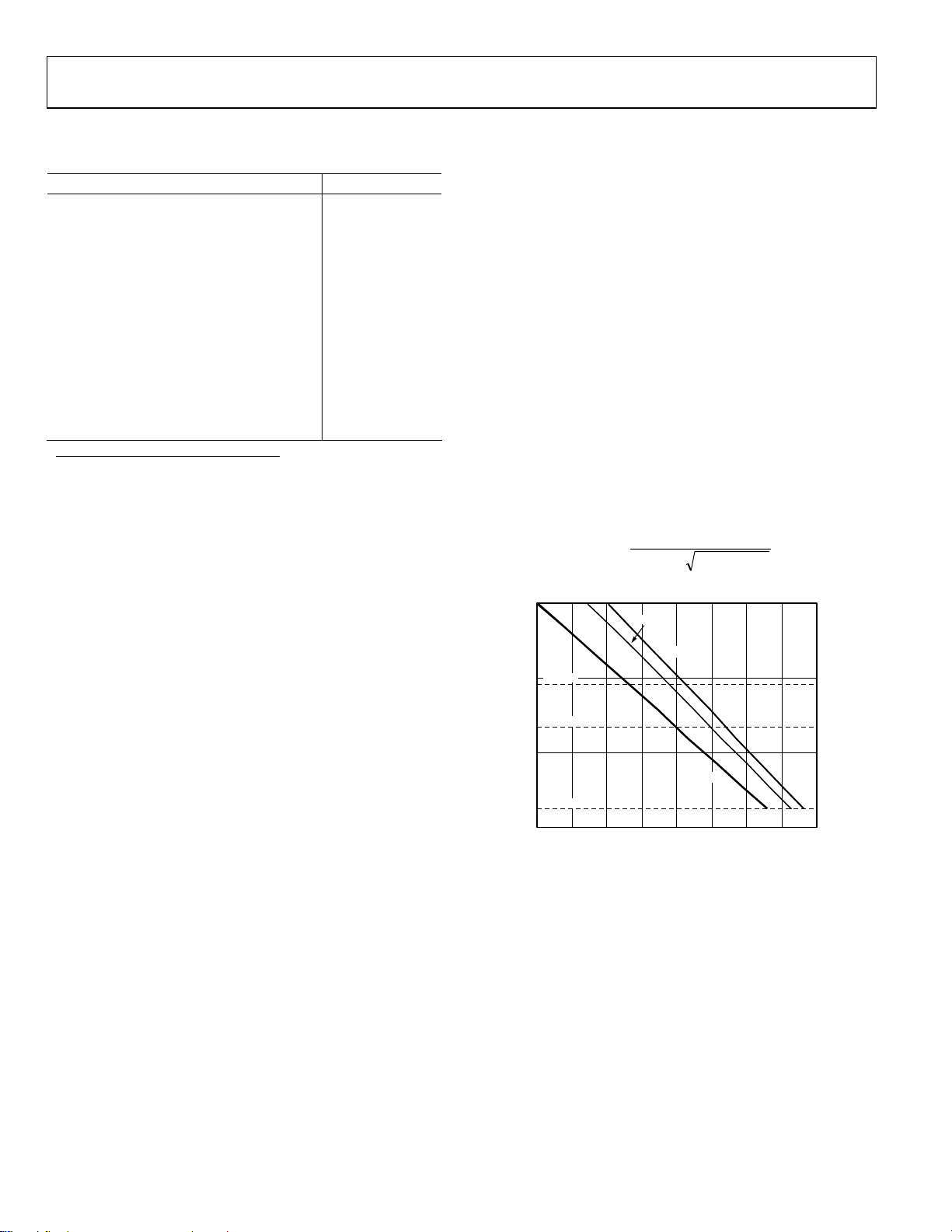
Note from the curve in Figure 20 that the AD8132 (Figure 18)
typically produces a symmetrical output at 85°C when its
supply, (V+) – (V–), is at 7.2 V.
AVCC = 15.5V
VZ = 5.1V
The V1 and V2 inputs in these systems are tied together and are
normally connected to VCOM, as shown in Figure 17.
VFS = 5V
AD8384
VCOM
V2
V1
VCOM
VBIAS = 1V
VBIAS = 1V
VFS = 5V
1023820
RESERVED
CODE
RANGE
Figure 17. V1, V2 Connection and Transfer Function
in a Typical Standard System
External Bias Voltage Generation
In systems that require improved brightness resolution and
higher accuracy, the V1 and V2 inputs, connected to external
voltage references, provide the necessary bias voltage (VBIAS)
while allowing the full code range to be used for gamma
correction.
To ensure a symmetrical ac voltage at the outputs of the
AD8384, VBIAS must remain constant for both states of INV.
Therefore, V1 and V2 are defined as
V1 = VCOM – VBIAS
V2 = VCOM + VBIAS
AD8384
V2
V1
04512-0-019
COM = 7V
R2 = 1kΩ
R1 = 6kΩ
1
–IN
V
COM
2
8
+IN
3
5
V+
AD8132
V–
6
DVCC = 3.3V
V2 = 8V
4
V1 = 6V
Figure 18. External VBIAS Generator with the AD8132
04512-0-018
VCOM
VFS = 4V
V2
V1
VFS = 4V
VBIAS = 1V
VBIAS = 1V
1023
04512-0-025
Figure 19. AD8384 Transfer Function in a Typical High Accuracy System
8.75
7.50
6.25
5.00
3.75
2.50
1.25
0.00
–1.25
–2.50
–3.75
(V2 + V1)/2 – VCOM (mV)
–5.00
–6.25
–7.50
–8.75
5.7 6.2 6.7 7.2 7.7 8.2 8.7 9.2 9.7 10.2 10.7
TA = 85°C
[V+] – [V–] (V)
TA = 25°C
04512-0-020
Figure 20. Typical Asymmetry at the Outputs of the AD8132 vs. Its Power
Supply for the Application Circuit
Rev. 0 | Page 18 of 24
Page 19

AD8384
PCB DESIGN FOR OPTIMIZED THERMAL PERFORMANCE
The AD8384’s total maximum power dissipation is partly load
dependent. In a 6-channel 60Hz XGA system running at a
65 MHz clock rate, the total maximum power dissipation is
1.6 W at a 150 pF LCD input capacitance.
At a clock rate of 100 MHz, the total maximum power
dissipation can exceed 2 W, as shown in Table 14, for a black-towhite video output voltage swing of 4 V and 5 V.
Table 14. Power Dissipation
V
C
LOAD
(pF)
150 1.12 0.82 1.94 0.71 1.83
200 1.12 1.01 2.13 0.86 1.98
250 1.12 1.21 2.33 1.01 2.13
300 1.12 1.41 2.53 1.17 2.29
P
(W)
QUIESCENT
P
DYNAMIC
(W)
Although the maximum safe operating junction temperature is
higher, the AD8384 is 100% tested at a junction temperature of
125°C. Consequently, the maximum guaranteed operating
junction temperature is 125°C. To limit the maximum junction
temperature at or below the guaranteed maximum, the package,
in conjunction with the PCB, must effectively conduct heat
away from the junction.
= 5 V V
SWING
P
TOTAL
(W)
= 4 V
SWING
P
P
DYNAMIC
(W)
TOTAL
(W)
A thermally effective PCB must incorporate two thermal pads
and a thermal via structure. The thermal pad on the top surface
of the PCB provides a solderable contact surface on the top
surface of the PCB. The thermal pad on the bottom PCB layer
provides a surface in direct contact with the ambient. The
thermal via structure provides a thermal path to the inner and
bottom layers of the PCB to remove heat.
THERMAL PAD DESIGN
To minimize thermal performance degradation of production
PCBs, the contact area between the thermal pad and the PCB
should be maximized. Therefore, the size of the thermal pad on
the top PCB layer should match the exposed paddle. The second
thermal pad of the same size should be placed on the bottom
side of the PCB. At least one thermal pad should be in direct
thermal contact with an external plane such as AVCC or GND.
THERMAL VIA STRUCTURE DESIGN
Effective heat transfer from the top to the inner and bottom
layers of the PCB requires thermal vias incorporated into the
thermal pad design. Thermal performance increases
logarithmically with the number of vias.
Near optimum thermal performance of production PCBs is
attained only when tightly spaced thermal vias are placed on the
full extent of the thermal pad.
The AD8384 package is designed to provide enhanced thermal
characteristics through the exposed die paddle on the bottom
surface of the package. In order to take full advantage of this
feature, the exposed paddle must be in direct thermal contact
with the PCB, which then serves as a heat sink.
Rev. 0 | Page 19 of 24
Page 20

AD8384
AD8384 PCB DESIGN RECOMMENDATIONS
Top PCB Layer
Land Pattern Dimensions
Pad Size: 0.6 mm × 0.25 mm
Pad Pitch: 0.5 mm
Thermal Pad Size: 6 mm × 6 mm
Thermal via structure: 0.25 mm to 0.35 mm diameter via holes on
a 0.5 mm to 1.0 mm grid.
14 mm
6 mm
14 mm
LAND PATTERN – TOP LAYER
Figure 21. Land Pattern—Top Layer
6 mm
6 mm
04512-0-021
Bottom PCB Layer
Thermal Pad and Thermal Via Connections
The thermal pad on the solder side is connected to a plane. Use of
thermal spokes is not recommended when connecting the thermal
pads or via structure to the plane.
Solder Masking
Solder masking of the via holes on the top layer of the PCB plugs
the via holes, inhibiting solder flow into the holes. To minimize the
formation of solder voids due to solder flowing into the via holes
(solder wicking), the via diameter should be made small and an
optional solder mask may be used. To optimize thermal pad
coverage, the solder mask’s diameter should be no more than
0.1 mm larger than the via hole diameter.
Solder Mask—Top Layer
Pads:
Set by the customer’s PCB design rules.
6 mm
LAND PATTERN – BOTTOM LAYER
Figure 22. Land Pattern—Bottom Layer
04512-0-022
Thermal Via Holes: Circular mask, centered on the via holes.
Diameter of the mask should be 0.1 mm larger than the via hole
diameter.
Solder Mask—Bottom Layer
Set by customer’s PCB design rules.
Rev. 0 | Page 20 of 24
SOLDER MASK – TOP LAYER
Figure 23. Solder Mask—Top Layer
04512-0-023
Page 21

AD8384
OUTLINE DIMENSIONS
PIN 1
14.00 SQ
12.00 SQ
TOP VIEW
(PINS DOWN)
61
60
61
60
BOTTOM
VIEW
80
1
6.00
SQ
0.75
0.60
0.45
SEATING
PLANE
1.20
MAX
80
1
0.15
0.05
COPLANARITY
0.20
0.09
0.08
20
21
1.05
1.00
0.95
0.50 BSC
0.27
0.22
0.17
COMPLIANT TO JEDEC STANDARDS MS-026-ADD-HD
41
40
GAGE PLANE
0.25
7°
3.5°
0°
41
40
Figure 24. 80-Lead, Thermally Enhanced Thin Quad Flatpack Package [TQFP]
(SV-80)
Dimensions shown in millimeters
ESD CAUTION
ESD (electrostatic discharge) sensitive device. Electrostatic charges as high as 4000 V readily
accumulate on the human body and test equipment and can discharge without detection. Although
this product features proprietary ESD protection circuitry, permanent damage may occur on devices
subjected to high energy electrostatic discharges. Therefore, proper ESD precautions are
recommended to avoid performance degradation or loss of functionality.
20
21
ORDERING GUIDE
Model Temperature Range Package Description Package Option
AD8384ASVZ11 0°C to 85°C 80-Lead Thin Quad Flat Pack SV-80
11
Z = Pb-free part.
Rev. 0 | Page 21 of 24
Page 22

AD8384
NOTES
Rev. 0 | Page 22 of 24
Page 23

AD8384
NOTES
Rev. 0 | Page 23 of 24
Page 24

AD8384
NOTES
© 2004 Analog Devices, Inc. All rights reserved. Trademarks and
registered trademarks are the property of their respective owners.
D04512–0–1/04(0)
Rev. 0 | Page 24 of 24
 Loading...