

Page 1
Low Cost 10-Bit, 6-Channel Output
FEATURES
High voltage drive to within 1.3 V of supply rails
Output short-circuit protection
High update rates
Fast, 100 Ms/s, 10-bit input data update rate
Low static power dissipation: 0.7 W
Includes STBY function
Voltage-controlled video reference (brightness) and
full-scale (contrast) output levels
INV bit reverses polarity of video signal
3.3 V logic, 9 V to 18 V analog supplies
High accuracy voltage outputs
Laser trimming eliminates the need for adjustments
Flexible logic
STSQ/XFR allow parallel AD8383 operation at various
resolutions
Fast settling into capacitive loads
30 ns settling time to 0.25% into 150 pF load
Slew rate 460 V/µs
Available in 48-lead 7 mm × 7 mm LFCSP package
APPLICATIONS
LCD analog column driver
PRODUCT DESCRIPTION
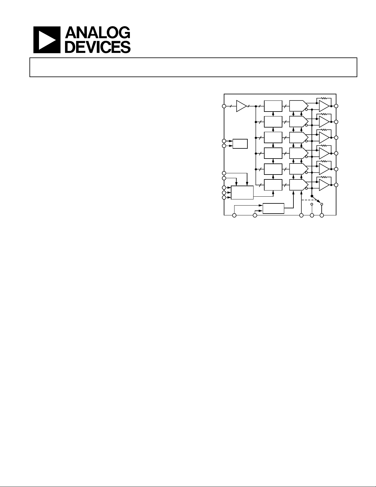
The AD8383 provides a fast, 10-bit latched decimating digital
input that drives six high voltage outputs. 10-bit input words are
sequentially loaded into six separate, high speed, bipolar DACs.
Flexible digital input format allows several AD8383s to be used
in parallel for higher resolution displays. STSQ synchronizes
sequential input loading, XFR controls synchronous output
updating, and R/L controls the direction of loading as either
left-to-right or right-to-left. Six channels of high voltage output
drivers drive to within 1.3 V of the rail. For maximum flexibility,
the output signal can be adjusted for dc reference, signal
inversion.
Decimating LCD DecDriver
AD8383
FUNCTIONAL BLOCK DIAGRAM
1010
10 10
DB(0:9)
STBY
BYP
R/L
E/O
CLK
STSQ
XFR
AD8383
SEQUENCE
CONTROL
VREFHI
BIAS
VREFLO
2-STAGE
LATCH
10 10
2-STAGE
LATCH
10 10
2-STAGE
LATCH
10 10
2-STAGE
LATCH
10 10
2-STAGE
LATCH
10 10
2-STAGE
LATCH
SCALING
CONTROL
Figure 1
The AD8383 is fabricated on the 26 V, fast bipolar XFHV
process developed by Analog Devices, Inc. This process
provides fast input logic, bipolar DACs with trimmed accuracy
and fast settling, high voltage, precision drive amplifiers on the
same chip.
The AD8383 dissipates 0.7 W nominal static power. The STBY
pin reduces power to a minimum with fast recovery.
The AD8383 is offered in a 48-lead, 7 mm × 7 mm × 0.85 mm
LFCSP package and operates over the commercial temperature
range of 0°C to 85°C.
DAC
DAC
DAC
DAC
DAC
DAC
INV V1 V2
VID0
VID1
VID2
VID3
VID4
VID5
®
04513-0-001
Rev. 0
Information furnished by Analog Devices is believed to be accurate and reliable.
However, no responsibility is assumed by Analog Devices for its use, nor for any
infringements of patents or other rights of third parties that may result from its use.
Specifications subject to change without notice. No license is granted by implication
or otherwise under any patent or patent rights of Analog Devices. Trademarks and
registered trademarks are the property of their respective owners.
One Technology Way, P.O. Box 9106, Norwood, MA 02062-9106, U.S.A.
Tel: 781.329.4700
Fax: 781.326.8703 © 2004 Analog Devices, Inc. All rights reserved.
www.analog.com
Page 2

AD8383
TABLE OF CONTENTS
Specifications..................................................................................... 3
Absolute Maximum Ratings............................................................ 5
Maximum Power Dissipation ..................................................... 5
Pin Configuration and Function Descriptions............................. 6
Timing Diagrams.............................................................................. 7
Theory of Operation ........................................................................ 8
Transfer Function and Analog Output Voltage ........................ 8
Applications....................................................................................... 9
External VBIAS Generation........................................................ 9
REVISION HISTORY
Revision 0: Initial Version
PCB Design for Good Thermal Performance........................ 10
Thermal Pad Design .................................................................. 10
Thermal Via Structure Design.................................................. 11
Solder Masking........................................................................... 11
Reference PCB Design............................................................... 11
Estimated Junction Temperature ............................................. 12
Outline Dimensions....................................................................... 14
Ordering Guide .......................................................................... 14
Rev. 0 | Page 2 of 16
Page 3

AD8383
SPECIFICATIONS
Table 1. @25°C, AVCC = 15.5 V, DVCC = 3.3 V, T
unless otherwise noted
Parameter Conditions Min Typ Max Unit
VIDEO DC PERFORMANCE
1
VDE –7.5 +7.5 mV
VCME –3.5 +3.5 mV
REFERENCE INPUTS
V1, V2 Range 5 AVCC – 4 V
V2 to V1 Range –0.25 V
V1 Input Current +0.2 µA
V2 Input Current –7.5 µA
VREFHI Range VREFHI ≥ VREFLO VREFLO AVCC V
VREFLO Range VREFHI ≥ VREFLO V1 – 0.5 AVCC – 1.3 V
VREFHI Input Resistance To VREFLO 20 kΩ
VREFLO Bias Current –0.2 µA
VREFHI Input Current 125 µA
VFS Range
2
RESOLUTION
Coding Binary 10 Bits
DIGITAL INPUT CHARACTERISTICS
Maximum Input Data Update Rate
3
CLK to Data Setup Time 0 ns
CLK to STSQ Setup Time 1 ns
CLK to XFR Setup Time 1 ns
CLK to Data Hold Time 3 ns
CLK to STSQ Hold Time 3 ns
CLK to XFR Hold Time 3 ns
CLK High Time 3 ns
CLK Low Time 2.5 ns
C
IN
I
IH
I
IL
IIL, CLK 1.2 µA
V
IH
V
IL
V
TH
VIDEO OUTPUT CHARACTERISTICS
Output Voltage Swing AVCC – VOH, VOL – AGND 1.1 1.3 V
CLK to VID Delay
4
INV to VID Delay 50% of VIDx 10.4 12.4 14.4 ns
Output Current 100 mA
Output Resistance 22 Ω
1
VDE = Differential Error Voltage = Common-Mode Error Voltage. See section. Theory of Operation
2
VFS = 2 × (VREFHI – VREFLO).
3
Maximum input transition time (10% to 90%) = 0.8/(2f) where f is the operating CLK rate.
4
Measured from 50% of falling CLK edge to 50% of output change. Measurement is made for both states of INV.
T
MIN
= 0°C, T
MIN
to T
, DAC Code 450 to 800
MAX
= 75°C, VFS = 5 V, VREFLO = V1 = V2 = 7 V,
MAX
0 5.5 V
100 Ms/s
3 pF
0.05 µA
0.6 µA
2 V
0.8 V
1.5 V
50% of VIDx 10.0 12.0 14.0 ns
Rev. 0 | Page 3 of 16
Page 4

AD8383
SPECIFICATIONS (continued)
Parameter Conditions Min Typ Max Unit
VIDEO OUTPUT DYNAMIC PERFORMANCE T
Data Switching Slew Rate 20% to 80% 460 V/µs
Invert Switching Slew Rate 20% to 80% 560 V/µs
Data Switching Settling Time to 1% 19 24 ns
Data Switching Settling Time to 0.25% 30 50 ns
Invert Switching Settling Time to 1% VO = 10 V Step 75 120 ns
Invert Switching Settling Time to 0.25% VO = 10 V Step 250 500 ns
Invert Switching Overshoot VO = 10 V Step 100 200 mV
CLK and Data Feedthrough
All-Hostile Crosstalk
5
6
Amplitude 40 mV p-p
Duration 20 ns
DAC Transition Glitch Energy Code 511 to Code 512 0.3 nV-s
POWER SUPPLY
DVCC, Operating Range 3 3.3 3.6 V
DVCC, Quiescent Current 20 28 mA
AVCC, Operating Range 9 18 V
Total AVCC Quiescent Current 40 48 mA
STBY AVCC Current STBY = H 0.15 0.45 mA
STBY DVCC Current STBY = H 3.5 5 mA
OPERATING TEMPERATURE RANGE, T
AMBIENT TEMPERATURE RANGE
OPERATING TEMPERATURE RANGE, T
A
7
J
5
Measured on two outputs differentially as CLK and DB(0:9) are driven and STSQ and XFR are held low.
6
Measured on two outputs differentially as the other four outputs make a full-scale transition for both states of INV.
7
Operation at 85°C ambient temperature requires a thermally optimized PCB layout (see Application Notes), minimum airflow of 200 lfm, input clock rate not
exceeding 100 MHz, black-to-white transition ≤4 V, C
C, MIN
to T
, VO = 5 V Step, CL = 150 pF
C, MAX
10 mV p-p
Ambient Temperature 0 75 °C
0 85 °C
100% tested 25 125 °C
≤150 pF.
L
Rev. 0 | Page 4 of 16
Page 5
AD8383
ABSOLUTE MAXIMUM RATINGS
Table 2. AD8383 Stress Ratings
Parameter Rating
Supply Voltages
AVCCx – AGNDx 18 V
DVCC – DGND 4.5 V
Input Voltages
Maximum Digital Input Voltages DVCC + 0.5 V
Minimum Digital Input Voltages DGND – 0.5 V
Maximum Analog Input Voltages AVCC + 0.5 V
Minimum Analog Input Voltages AGND – 0.5 V
Internal Power Dissipation
LFCSP Package @ 25°C Ambient 3.8 W
Operating Temperature Range 0°C to 85°C
Storage Temperature Range –65°C to +125°C
Lead Temperature Range (Soldering 10 sec) 300°C
8
Stresses above those listed under the Absolute Maximum
Ratings may cause permanent damage to the device. This is a
stress rating only; functional operation of the device at these or
any other conditions above those indicated in the operational
section of this specification is not implied. Exposure to the
absolute maximum ratings for extended periods may reduce
device reliability.
8
48-Lead LFCSP Package:
= 26°C/W (Still Air): JEDEC STD, 4-layer board with 0 CFM airflow
θ
JA
= 20°C/W
θ
JC
= 11.0°C/W in Still Air
ψ
JB
MAXIMUM POWER DISSIPATION
Junction Temperature
The maximum power that can be safely dissipated by the
AD8383 is limited by its junction temperature. The maximum
safe junction temperature for plastic encapsulated devices as
determined by the glass transition temperature of the plastic is
approximately 150°C. Exceeding this limit temporarily may
cause a shift in the parametric performance due to a change in
the stresses exerted on the die by the package. Exceeding a
junction temperature of 175°C for an extended period can
result in device failure.
Overload Protection
The AD8383 employs a 2-stage overload protection circuit that
consists of an output current limiter and a thermal shutdown.
The maximum current at any one output of the AD8383 is
internally limited to 100 mA, average. In the event of a momentary short-circuit between a video output and a power supply
rail (AVCC or AGND), the output current limit is sufficiently
low to provide temporary protection.
The thermal shutdown debiases the output amplifier when the
junction temperature reaches the internally set trip point. In the
event of an extended short-circuit between a video output and a
power supply rail, the output amplifier current continues to
switch between 0 mA and 100 mA typical with a period
determined by the thermal time constant and the hysteresis of
the thermal trip point. The thermal shutdown provides longterm protection by limiting the average junction temperature to
a safe level.
Operating Temperature Range
Production testing guarantees a minimum thermal shutdown
junction temperature (T
) of at least 125°C.
J
To ensure operation at T
maximum power dissipation as described in the Applications
section.
Exposed Paddle
The die paddle must be soldered to AVCC for reliable electrical
operation.
See the Applications section for details regarding use of the
exposed paddles to dissipate excess heat.
ESD CAUTION
ESD (electrostatic discharge) sensitive device. Electrostatic charges as high as 4000 V readily
accumulate on the human body and test equipment and can discharge without detection. Although
this product features proprietary ESD protection circuitry, permanent damage may occur on devices
subjected to high energy electrostatic discharges. Therefore, proper ESD precautions are
recommended to avoid performance degradation or loss of functionality.
Rev. 0 | Page 5 of 16
< 125°C, it is necessary to limit the
J
Page 6

AD8383
PIN CONFIGURATION AND FUNCTION DESCRIPTIONS
CLK
XFR
STSQNCNC
4847464544
V1
AVCCDAC
AGNDDACVREFHI
4342414039
VREFLO
V2
38
AGND0
37
1
NC
DB0
2
DB1
3
DB2
4
DB3
5
DB4
6
DB5
7
DB6
8
DB7
9
10
DB8
11
DB9
NC
12
13
E/O
NC = NO CONNECT
PIN 1
INDICATOR
14
R/L
(Not to Scale)
15
16
INV
DGND
AD8383
TOP VIEW
7mm × 7mm
17
18NC19
DVCC
AVCCBIAS
20
STBY
21
22
BYP
AGNDBIAS
23
NC
24
NC
36
35
34
33
32
31
30
29
28
27
26
25
VID0
AVCC0,1
VID1
AGND1,2
VID2
AVCC2,3
VID3
AGND3,4
VID4
AVCC4,5
VID5
AGND5
04513-0-002
Figure 2. 48-Lead LFCSP Pin Configuration
Table 3. Pin Function Descriptions
Pin Name Function Description
DB(0:9) Data Input 10-Bit Data Input. MSB = DB(0:9).
CLK Clock Clock Input.
STSQ Start Sequence
The state of STSQ is detected on the active edge of CLK. A new data loading sequence begins on
the next active edge of CLK after STSQ is detected HIGH.
The active CLK edge is the rising edge when E/O is held HIGH. It is the falling edge when E/O is
held LOW.
R/L Right/Left Select
A new data loading sequence begins on the left with Channel 0 when this input is LOW, and on
the right with Channel 5 when this input is HIGH.
E/O Even/Odd Select
The active CLK edge is the rising edge when this input is held HIGH and the falling edge when
this input is held LOW. Data is loaded sequentially on the rising edges of CLK when this input is
HIGH and on the falling edges when this input is LOW.
XFR Data Transfer
XFR is detected and a data transfer is initiated on a rising CLK edge when this input is held HIGH.
Data is transferred to the video outputs on the next rising CLK edge after XFR is detected.
VID0–VID5 Analog Outputs These pins are directly connected to the analog inputs of the LCD panel.
V1, V2 Reference Voltages The voltage applied between these pins set the reference levels of the analog outputs.
VREFHI,
Full-Scale References The voltage applied between these pins sets the full-scale output voltage.
VREFLO
INV Invert
When this pin is HIGH, the analog output voltages are above VMID. When LOW, the analog
output voltages are below VMID. VMID is a hypothetical reference level set by the voltages
applied to V1 and V2. VMID is equal to (V1 + V2)/2.
DVCC Digital Power Supply Digital Power Supply.
DGND Digital Supply Return This pin is normally connected to the analog ground plane.
AVCCx Analog Power Supplies Analog Power Supplies.
AGNDx Analog Supply Returns Analog Supply Returns.
BYP Bypass A 0.1 µF capacitor connected between this pin and AGND ensures optimum settling time.
STBY Standby When HIGH, the internal circuits are debiased and the power dissipation drops to a minimum.
Rev. 0 | Page 6 of 16
Page 7

AD8383
TIMING DIAGRAMS
t
CLK LOW
t
CLK HIGH
V
TH
V
TH
= 1.65V
= 1.65V
04513-0-003
CLK
DB(0:9)
STSQ
XFR
CLK
DB(0:9)
t
CLK HIGH
VTH = 1.65V
t
HOLD
V
TH
t
HOLD
= 1.65V
t
SKEW
t
SETUP
t
SETUP
Figure 3. Timing Diagram, Even Mode (E/O = HIGH)
t
CLK LOW
V
= 1.65V
TH
t
t
SKEW
SETUP
V
TH
t
HOLD
= 1.65V
STSQ
XFR
t
SETUP
t
HOLD
SETUP
t
HOLD
V
V
= 1.65V
TH
= 1.65V
TH
04513-0-004
t
Figure 4. Timing Diagram, Odd Mode (E/O = LOW)
Rev. 0 | Page 7 of 16
Page 8

AD8383
[
THEORY OF OPERATION
TRANSFER FUNCTION AND ANALOG OUTPUT VOLTAGE
The DecDriver has two regions of operation: where the video
output voltages are either above or below a reference voltage
VMID, and where VMID = (V1 + V2)/2. The transfer function
defines the analog output voltage as the function of the digital
input code as follows:
n
–1)(
–1)(
⎞
for INV = LOW
⎟
1023
⎠
n
⎞
for INV = HIGH
⎟
1023
⎠
⎛
×=
FSV – V1nVIDx
⎜
⎝
⎛
×+=
VFS2VnVIDx
⎜
⎝
To best correlate transfer function errors to image artifacts, the
overall accuracy of the DecDriver is defined by two parameters,
VDE and VCME.
VDE, the differential error voltage, measures the difference
between the rms value of the output and the rms value of the
ideal. The defining expression is
nVDE ×
=
)(
][ ]
2
−−−
)()(
n1VnVOUTP2VnVOUTN
−−
1023
⎞
⎟
⎠
⎛
1
⎜
⎝
VFS
where n = input code
VFS = 2 × (VREFHI – VREFLO)
A number of internal limits define the usable range of the
analog output voltages, VIDx, as shown in Figure 5.
AVCC
2V
V2 + V
FS
V2
V
MID
VIDx (V)
V1
V1 – V
FS
AGND
Figure 5. Transfer Function, VIDx vs. Input Code, Internal Limits and Usable Output Voltage Range
REFHI–VREFLO
INV = HIGH
V
= (V1+V2)/2
MID
INV = LOW
0 1023
INPUT CODE
VCME, the common-mode error voltage, measures ½ the dc
bias of the output. The defining expression is
1
⎡
≥ 1.3V
0 ≤ VFS≤ 5.5V
5V ≤ V2 ≤ (AVCC – 4)
0 ≤ VFS≤ 5.5V
≥ 1.3V
INTERNAL LIMITS AND
USABLE VOLTAGE RANGES
)(
⎢
212
⎣
9V ≤ AVCC ≤ 18V
5V ≤ V1 ≤
(AVCC – 4)
()
04513-0-005
+=
–)()(
nVOUTPnVOUTNnVCME
+
2V1V
⎤
⎥
2
⎦
Rev. 0 | Page 8 of 16
Page 9

AD8383
V
APPLICATIONS
The V1 and V2 inputs in these systems are tied together and are
normally connected to VCOM, as shown in Figure 6.
AD8383
VCOM
V2
V1
04513-0-006
Figure 6. Standard Connection Diagram
The transfer function of the AD8383 is shown in Figure 7 for
V2 = V1 = VCOM.
VFS = 5V
VCOM
VBIAS = 1V
VBIAS = 1V
VFS = 5V
1023820
RESERVED
CODE
RANGE
COM = 7V
R2 = 1kΩ
R1 = 6kΩ
AVCC = 15.5V
VZ = 5.1V
–IN
V+
VCOM
AD8132
V–
+IN
DVCC = 3.3V
3
5
4
6
V2 = 8V
V1 = 6V
V2
V1
1
2
8
Figure 8. High Accuracy Reference Circuit
VFS = 4V
V2
VCOM
V1
VFS = 4V
VBIAS = 1V
VBIAS = 1V
1023
AD8383
04513-0-008
04513-0-007
Figure 7. Output Transfer Function for Standard Connection
EXTERNAL VBIAS GENERATION
In systems that require improved brightness resolution and
higher accuracy, the V1 and V2 inputs, connected to external
voltage references, provide the necessary VBIAS while allowing
the full code range to be used for gamma correction.
V1 sets the white drive voltage while INV = LOW and V2 sets
the white drive voltage while INV = HIGH. V1 and V2 are
defined as
V1 = VCOM – VBIAS
V2 = VCOM + VBIAS
To ensure a symmetrical ac driving voltage, the difference
between V2 and VCOM must be equal to the difference
between VCOM and V1.
(V2 – VCOM) = (VCOM – V1)
The circuit in Figure 8 ensures symmetry to within 1 mV with a
minimum component count. Bypass capacitors are not shown
for clarity.
The transfer function and the input symmetry error of the
AD8383 are shown in Figure 9 when the circuit of Figure 8 is
used to generate VBIAS.
THE AD8383, IN THE APPLICATIONS
CIRCUIT SHOWN, TYPICALLY PRODUCES
A SYMMETRICAL OUTPUT AT 85°C WHEN
ITS SUPPLY, (V+) – (V–), IS AT 7.2V.
04513-0-009
Figure 9. Transfer Function for High Accuracy Reference Applications
8.75
7.50
6.25
5.00
3.75
2.50
1.25
0.00
–1.25
–2.50
–3.75
(V2 + V1)/2 – VCOM (mV)
–5.00
–6.25
–7.50
–8.75
TYPICAL ASYMMETRY AT THE OUTPUTS OF THE
AD8383 VERSUS ITS POWER SUPPLY FOR THE
APPLICATION CIRCUIT
5.7 6.2 6.7 7.2 7.7 8.2 8.7 9.2 9.7 10.2 10.7
TA = 85°C
V
+
– V– (V)
TA = 25°C
Figure 10. Accuracy for High Accuracy Reference Applications
04513-0-010
Rev. 0 | Page 9 of 16
Page 10

AD8383
PCB DESIGN FOR GOOD THERMAL PERFORMANCE
The total maximum power dissipation of the AD8383 is partly
dependent on load. In a 6-channel 60 Hz XGA system running
at a 65 MHz clock rate, the total maximum power dissipation is
1.08 W at an LCD panel input capacitance of 150 pF.
At the maximum specified clock rate of 100 Ms/s, the total
maximum power dissipation can exceed 2 W for large capacitive
loads, as shown in Table 4.
Although the maximum safe operating junction temperature is
higher, the AD8383 is 100% tested at a junction temperature of
125°C. Consequently, the maximum guaranteed operating
junction temperature is 125°C. To limit the maximum junction
temperature at or below the guaranteed maximum, the package,
in conjunction with the PCB, must effectively conduct heat
away from the junction.
The AD8383’s LFCSP package is designed to provide superior
thermal characteristics, partly achieved by an exposed die
paddle on the bottom surface of the package. In order to take
full advantage of this feature, the exposed paddle must be in
direct thermal contact with the PCB, which then serves as a
heat sink.
THERMAL PAD DESIGN
Thermal performance of the AD8383 varies logarithmically
with the contact area between the exposed thermal paddle and
the thermal pad on the top layer of the PCB. See Figure 11.
The θ
(of the AD8383 mounted on a standard JEDEC PCB) is
JA
reduced by approximately 40% as the contact area increases
from 0% (no thermal pad) to 50%. It approaches its specified
value as the contact area (on the JEDEC standard PCB)
approaches 100%.
In order to minimize thermal performance degradation of
production PCBs, the contact area between the thermal pad and
the PCB should be maximized. Therefore, the size of the
thermal pad should match the exposed 5.25 mm × 5.25 mm
paddle size. However, if the PCB design rules require a pad-topad clearance of more than 0.3 mm, the size of the thermal pad
may be reduced to 5 mm × 5 mm. Additionally, a second
thermal pad of the same size should be placed on the bottom
side of the PCB. At least one thermal pad should be in direct
thermal (and electrical) contact with the AVCC plane.
50
A thermally effective PCB must incorporate a thermal pad and
45
a thermal via structure. The thermal pad provides a solderable
contact surface on the top surface of the PCB. The thermal via
structure provides a thermal path to the inner and bottom
layers of the PCB to remove heat.
40
(°C/W)
JA
θ
35
30
25
Figure 11. Thermal Performance vs. Contact Area (on a JEDEC PCB)
250 50 75 100
CONTACT AREA (%)
04513-0-011
Table 4. Power Dissipation vs. Load Capacitance and VFS at 100 Ms/s Clock Rate
VFS = 5 V VFS = 4 V
C
(pF) P
LOAD
QUIESCENT
(W) P
(W) P
DYNAMIC
(W) P
TOTAL
(W) P
DYNAMIC
TOTAL
(W)
150 0.7 0.72 1.42 0.58 1.28
200 0.7 0.96 1.66 0.77 1.47
250 0.7 1.20 1.90 0.96 1.66
300 0.7 1.44 2.14 1.15 1.85
Rev. 0 | Page 10 of 16
Page 11

AD8383
THERMAL VIA STRUCTURE DESIGN
Effective heat transfer from the top to the inner and bottom
layers of the PCB requires thermal vias incorporated into the
thermal pad design. Thermal performance increases logarithmically with the number of vias, as shown in Figure 12. With the
AD8383 on a standard JEDEC PCB, θ
value when a total of 16 vias are used. At a via count above 36,
approaches its optimum value as the slope of the curve
θ
JA
approaches zero.
32
30
28
(°C/W)
JA
θ
26
24
reaches its specified
JA
REFERENCE PCB DESIGN
The top copper layer is shown in Figure 13.
7 mm
7 mm
Figure 13. Recommended PCB Landing
The bottom thermal pad forms AVCC plane.
04513-0-013
22
Figure 12. Thermal Performance vs. Number of Vias (on a JEDEC PCB)
1002030
NUMBER OF VIAS
40
04513-0-012
Near optimum thermal performance of production PCBs is
attained when the number of vias is at least 36.
SOLDER MASKING
To minimize the formation of solder voids due to solder flowing
into the via holes (solder wicking), the via diameter should be
small. Solder masking of the via holes on the top layer of the
PCB plugs the via holes, inhibiting solder flow into the holes. To
optimize the thermal pad coverage, the solder mask diameter
should be no more than 0.1 mm larger than the via diameter.
Thermal Pads
Top PCB Layer: 5.25 mm × 5.25 mm
Bottom PCB Layer: 5.25 mm × 5.25 mm
Thermal via structure
Diameter: 0.25 mm
Number of vias: 41
Via Grid Pitch: 0.5 mm
Miscellaneous
Perimeter Pads: 0.5 mm × 0.25 mm
Solder Mask Swell: 0.02 mm
Rev. 0 | Page 11 of 16
Page 12

AD8383
θ
+
(
(
θ, ψ
θJB, ψ
JB
θ
AD8383
CP
T
J
JC
C
JC
θ
JC-BOTTOM
C
JC-BOTTOM
Figure 14. Thermal Equivalent Circuit
ESTIMATED JUNCTION TEMPERATURE
Assuming no heat flows through the sides of the AD8383 package, heat flow from the AD8383 is through two paths. While
part of the total heat generated dissipates through the top of the
case, the remainder flows into the PCB to be dissipated.
Assuming there is no other heat-generating component near the
AD8383, the thermal equivalent circuit of a system that consists
of one AD8383 mounted on a PCB is shown in Figure 14.
The thermal resistance of the top of the case, θ
independent of the system variables, and well defined. θ
depends on the thermal resistance of the molding compound.
, is constant,
JC
JC
C
θ
PCB
PCB
θ
AIR-CASE
T
PCB
T
CASE
PCB
C
AIR-CASE
θ
AIR-PCB
C
AIR-PCB
T
T
A
AMBIENT
04513-0-014
Junction Temperature and Maximum Power Dissipation
In a thermal steady state represented by the simplified schematic shown in Figure 15, heat flow from the die is partly through
the top of the case, causing a temperature drop (T
partly through the PCB, causing a temperature drop (T
The junction temperature is calculated as follows:
TT
CASEJ
PCBCASE
PPP
J
=
T
−
=+=
JC
θ
PCBJC
θ θ
+
TT
−
+
CBP
θ
Tθ T θ Pθθ
PCBJCCASEPCBPCBJC
+
J
PCBJ
– T
)()(
CASE
J
), and
– T
PCB
).
The thermal resistance of the system, θ
, is system dependent
JA
and therefore cannot be properly estimated. Although it is traditional to provide the thermal resistance of a JEDEC reference
system in the data sheet, its value may not be appropriate for all
systems and may result in large errors (>>25%).
The thermal resistance of production PCBs, θ
, depends largely
JC
on the particular PCB design, and, to some extent, the environmental conditions specific to the particular system. Although θ
is traditionally not provided on data sheets, a thermal characterization parameter, ψ
, of a JEDEC reference system is gaining
JB
increasing acceptance. When the PCB thermal design near the
AD8383 closely approximates the PCB of the JEDEC reference
system, θ
approaches ψJB.
JA
For thermally enhanced packages, the thermal resistance of the
exposed thermal paddle, θ
JC-BOTTOM
, is very low and may
therefore be ignored.
where:
T
is the junction temperature
J
is the temperature of the top of the case (near the output
T
CASE
pins for the AD8383)
is the PCB temperature on the solder side (directly under
T
PCB
the AD8383)
P is the total power dissipated by the AD8383
JB
is the thermal resistance of the top of the case
θ
JC
is the thermal resistance of the PCB
θ
PCB
At a given maximum allowed junction temperature, the
maximum allowed power dissipation is
+
θ θ
⎡
=
P
MAX
⎢
⎣
PCBJC
PCBJC
θθ
For a thermally optimized PCB,
)
T
JMAX
θ
can be replaced with ψ
JC
T
T
θ
CASE
JC
PCB
⎤
−−
⎥
PCB
θ
⎦
PCB
and the equation can be rewritten as
P
MAX
⎡
=
⎢
⎣
)
PCBJC
ψ θ
+
ψθ
JMAX
T
PCBJC
CASE
T
JC
θ
⎤
PCB
T
−−
⎥
PCB
ψ
⎦
Rev. 0 | Page 12 of 16
Page 13

AD8383
θ
P
PCB
θ
PCB
T
PCB
AIR-PCB
Figure 15. Simplified Thermal Equivalent Circuit
P
T
J
T
A
P
P
C
θ
JC
T
CASE
θ
AIR-CASE
04513-0-015
Verification of the Maximum Operating Junction Temperature
In order to verify the system thermal design for compliance
with the maximum operating junction temperature specification, temperature measurements T
CASE
and T
are required at
PCB
the maximum possible total power dissipation in a complete,
fully assembled LCD projection system.
Maximum possible total power dissipation of the AD8383
occurs when the video input to the projector is a pattern with
1-pixel-wide white and black vertical lines. An alternative
pattern that results in the maximum possible total power
dissipation is a 1-pixel checkerboard pattern. The expected total
power dissipation of the AD8383 in a 60 Hz, 6-channel XGA
projector displaying the 1-pixel-wide vertical line or checkerboard pattern is 1.08 W (at AVCC = 15.5 V, VCOM = 7 V, and
LCD capacitance = 150 pF).
Although the case and PCB temperatures are highly dependent
on the PCB design, their measured values are expected to be
similar at approximately 40°C above the ambient (on a typical
PCB with a minimal airflow whose thermal design follows the
recommendations described in this note). The junction temperature then calculates to approximately 10°C above the case and
PCB temperatures. At a 70°C ambient temperature, the junction
temperature is expected to be at approximately 120°C.
The AD8383 has a relatively small thermal mass. In order to
minimize measurement errors due to the thermal mass of the
measuring device, a small-gauge thermocouple or a thermal
probe with a very small thermal mass is required for the measurement of T
CASE
and T
PCB
.
Power-Up and Power-Down Sequencing
As indicated in the Absolute Maximum Ratings, the voltage at
any input pin cannot exceed its supply voltage by more than
0.5 V. To ensure compliance with the Absolute Maximum
Ratings, power-up and power-down sequencing may be
required.
During power-up, initial application of nonzero voltages to any
of the input pins must be delayed until the supply voltage ramps
up to at least the highest maximum operational input voltage.
During power-down, the voltage at any input pin must reach
zero during a period not exceeding the hold-up time of the
power supply.
Failure to comply with the Absolute Maximum Ratings may
result in functional failure or damage to the internal ESD
diodes.
Damaged ESD diodes may cause temporary parametric failures,
which may result in image artifacts. Damaged ESD diodes
cannot provide full ESD protection, thus reducing reliability.
The recommended sequence is
Power ON
1. Apply power to supplies.
2. Apply power to other I/Os.
Power OFF
1. Remove power from I/Os.
2. Remove power from supplies.
VBIAS Generation—V1, V2 Input Pin Functionality
In order to avoid image flicker, a bias voltage of approximately
1 V minimum must be maintained across the pixels of HTPS
LCDs. The AD8383 provides two methods of maintaining this
bias voltage.
Internal Bias Voltage Generation
Standard systems that internally generate the bias voltage
reserve the upper-most code range for the bias voltage and use
the remaining code range to encode the video for gamma
correction.
Rev. 0 | Page 13 of 16
Page 14

AD8383
OUTLINE DIMENSIONS
BSC SQ
PIN 1
INDICATOR
7.00
0.60 MAX
37
36
0.60 MAX
0.30
0.23
0.18
PIN 1
48
INDICATOR
1
5.25
5.10 SQ
4.95
12
13
0.25 MIN
1.00
0.85
0.80
12° MAX
SEATING
PLANE
TOP
VIEW
0.80 MAX
0.65 TYP
0.50 BSC
COMPLIANT TO JEDEC STANDARDS MO-220-VKKD-2
6.75
BSC SQ
0.20 REF
0.50
0.40
0.30
0.05 MAX
0.02 NOM
COPLANARITY
25
0.08
BOTTOM
VIEW
24
5.50
REF
Figure 16. 48-Lead Frame Chip Scale Package [LFCSP]
(CP-48)
Dimensions shown in millimeters
ORDERING GUIDE
Model Temperature Range Package Description Package Option
AD8383ACPZ
9
Z = Pb-free part.
9
0°C to 85°C 48-Lead LFCSP CP-48
Rev. 0 | Page 14 of 16
Page 15

AD8383
NOTES
Rev. 0 | Page 15 of 16
Page 16

AD8383
NOTES
© 2004 Analog Devices, Inc. All rights reserved. Trademarks and
registered trademarks are the property of their respective owners.
D03191–0–1/04(0)
Rev. 0 | Page 16 of 16
 Loading...