

Page 1
High Performance 12-Bit, 6-Channel Output,
V
V
V
V
V
V
PRODUCT FEATURES
High accuracy, high resolution voltage outputs
12-bit input resolution
Laser trimmed outputs
Fast settling, high voltage drive
33 ns settling time to 0.25% into 200 pF load
Slew rate 390 V/µs
Outputs to within 1.3 V of supply
High update rates
Fast, 120 Ms/s data update rate
Voltage controlled video reference (brightness) and
full-scale (contrast) output levels
Flexible logic
STSQ/XFR allow parallel AD8382 operation
INV bit reverses polarity of video signal
Output overload protection
Low static power dissipation: 743 mW
Includes STBY function
3.3 V logic, 9 V to 18 V analog supplies
Available in 48-lead 7 mm × 7 mm LFCSP
APPLICATIONS
LCD analog column driver
Decimating LCD DecDriver
AD8382
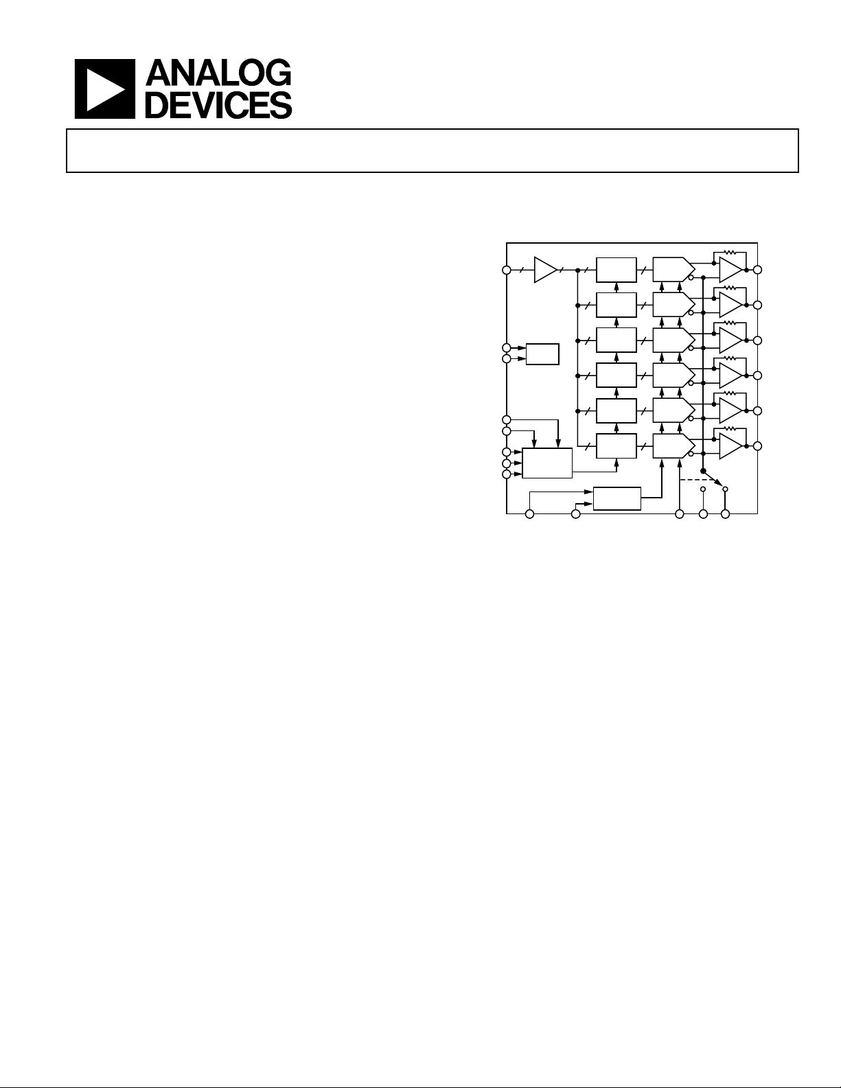
FUNCTIONAL BLOCK DIAGRAM
12 12
1212
DB(0:11)
STBY
BYP
R/L
E/O
CLK
STSQ
XFR
2-STAGE
LATCH
12 12
AD8382
SEQUENCE
CONTROL
VREFHI
BIAS
VREFLO
2-STAGE
LATCH
12 12
2-STAGE
LATCH
12 12
2-STAGE
LATCH
12 12
2-STAGE
LATCH
12 12
2-STAGE
LATCH
SCALING
CONTROL
Figure 1. Functional Block Diagram
DAC
DAC
DAC
DAC
DAC
DAC
INV V1 V2
®
ID0
ID1
ID2
ID3
ID4
ID5
PRODUCT DESCRIPTION
The AD8382 DecDriver provides a fast, 12-bit latched decimating digital input that drives six high voltage outputs.12-bit input
words are sequentially loaded into six separate, high speed,
bipolar DACs. A flexible digital input format allows several
AD8382s to be used in parallel for higher resolution displays.
STSQ synchronizes sequential input loading, XFR controls
synchronous output updating, and R/L controls the direction of
loading as either left-to-right or right-to-left. Six channels of
high voltage output drivers drive to within 1.3 V of the rail. The
output signal can be adjusted for dc reference, signal inversion,
and contrast for maximum flexibility.
The AD8382 is fabricated on Analog Devices’ XFHV, fast
bipolar 26 V process, providing fast input logic bipolar DACs
with trimmed accuracy and fast settling, high voltage, precision
drive amplifiers on the same chip. The AD8382 dissipates
743 mW nominal static power. The STBY pin reduces power to
a minimum, with fast recovery.
Rev. 0
Information furnished by Analog Devices is believed to be accurate and reliable.
However, no responsibility is assumed by Analog Devices for its use, nor for any
infringements of patents or other rights of third parties that may result from its use.
Specifications subject to change without notice. No license is granted by implication
or otherwise under any patent or patent rights of Analog Devices. Trademarks and
registered trademarks are the property of their respective companies.
One Technology Way, P.O. Box 9106, Norwood, MA 02062-9106, U.S.A.
Tel: 781.329.4700
Fax: 781.326.8703 © 2003 Analog Devices, Inc. All rights reserved.
www.analog.com
Page 2

AD8382
TABLE OF CONTENTS
Specifications..................................................................................... 3
Applications..................................................................................... 15
Absolute Maximum Ratings............................................................ 5
Timing Characteristics..................................................................... 6
Pin Configuration and Functional Descriptions.......................... 7
Typical Performance Characteristics ............................................. 8
Functional Description.................................................................. 13
Transfer Function ....................................................................... 13
Accuracy ...................................................................................... 14
REVISION HISTORY
Revision 0: Initial Version
VBIAS Generation—V1, V2 Input Pin Functionality ........... 17
Power Supply Sequencing ......................................................... 18
PCB Design for Optimized Thermal Performance ............... 18
Layout Considerations............................................................... 20
Outline Dimensions....................................................................... 21
Ordering Guide .......................................................................... 21
Rev. 0 | Page 2 of 24
Page 3

AD8382
SPECIFICATIONS
Table 1. @ 25°C, AVCC = 15.5 V, DVCC = 3.3 V, T
otherwise noted.
Parameter Conditions Min Typ Max Unit
VIDEO DC PERFORMANCE1 T
VDE DAC Code 1500 to 3200 –5 +5 mV
VCME DAC Code 1500 to 3200 –3.5 +0.5 +3.5 mV
∆V
∆V
VIDEO OUTPUT DYNAMIC PERFORMANCE T
Data Switching Slew Rate 20% to 80% 390
Invert Switching Slew Rate 20% to 80% 530
Data Switching Settling Time to 1% 22 27 ns
Data Switching Settling Time to 0.25% 33 50 ns
Invert Switching Settling Time to 1% 34 100 ns
Invert Switching Settling Time to 0.25% 130 300 ns
Invert Switch Overshoot 100 200 mV
CLK and Data Feedthrough2 10 mV p-p
All-Hostile Crosstalk3
Amplitude 40 mV p-p
Duration 30 ns
DAC Transition Glitch Energy Code 2047 to Code 2048 0.3 nV-s
VIDEO OUTPUT CHARACTERISTICS
Output Voltage Swing AVCC – VOH, VOL– AGND 1.1 1.3 V
CLK to VID Delay: t
INV to VID Delay: t10 50% of VIDx 10.4 12.4 14.4 ns
Output Current 100 mA
Output Resistance 22
RESOLUTION
Coding Binary 12 Bits
DIGITAL INPUT CHARACTERISTICS Input tr, tf = 2 ns (10% to 90%)
Max. Input Data Update Rate 120 Ms/s
Data Setup Time: t1 0 ns
STSQ Setup Time: t3 1 ns
XFR Setup Time: t5 1 ns
Data Hold Time: t2 3 ns
STSQ Hold Time: t4 3 ns
XFR Hold Time: t6 3 ns
CLK High Time: t7 3 ns
CLK Low Time: t8 2.5 ns
CIN 3 pF
IIH 0.05
IIL—All Inputs except CLK 0.6
IIL—CLK 1.2
VIH 2 V
VIL 0.8 V
VTH 1.6 V
4
50% of VIDx 10 12 14 ns
9
MIN
= 0°C, T
MIN
to T
MAX
= 85°C, VREFHI = 9.5 V, VREFLO = V1 = V2 = 7 V, unless
MAX
DAC Code 2048 2.5 7.5 mV
DAC Code 0 to 4095 4 15 mV
to T
C, MIN
V
= 5 V Step, CL = 200 pF
O
C, MAX
,
V/µs
V/µs
Ω
µA
µA
µA
Rev. 0 | Page 3 of 24
Page 4

AD8382
Parameter Conditions Min Typ Max Unit
REFERENCE INPUTS1
V1 Range
V2 Range
V2 ≥ (V1 – 0.25 V)
V2 ≥ (V1 – 0.25 V)
V1 Input Current 0.2
V2 Input Current –7.5
VREFLO Range
VREFHI Range
VREFHI ≤ (VREFLO + 2.75 V)
VREFHI ≤ (VREFLO + 2.75 V)
(VREFHI – VREFLO) Range 0 2.75 V
VREFHI Input Resistance 20
VREFLO Bias Current –0.2
VREFHI Input Current 125
VFS Range
VFS = 2 × (VREFHI – VREFLO)
POWER SUPPLY
DVCC, Operating Range 3 3.3 3.6 V
DVCC, Quiescent Current 23 31 mA
AVCC, Operating Range 9 18 V
Total AVCC Quiescent Current 43 52 mA
STBY AVCC Current STBY = HIGH 0.15 0.45 mA
STBY DVCC Current STBY = HIGH 3.5 5 mA
OPERATING TEMPERATURE RANGE
Ambient Temperature Range, TA Still Air 0 75 °C
Ambient Temperature Range, T
5
0 85 °C
A
Junction Temperature Range, TJ 100% Tested 25 125 °C
5 AVCC – 4 V
5 AVCC – 4 V
µA
µA
V1 – 0.5 AVCC – 1.3 V
VREFLO AVCC V
kΩ
µA
µA
5.5 V
1
VDE = differential error voltage. VCME = common-mode error voltage. ∆V = maximum deviation between outputs.
Full-scale output voltage = VFS = 2 × (VREFHI – VREFLO). See the Accu section on page 14. racy
2
Measured on two outputs differentially as CLK and DB(0:11) are driven and STSQ and XFR are held LOW.
3
Measured on two outputs differentially as the other four are transitioning by 5 V. Measured for both states of INV.
4
Measured from 50% of falling CLK edge to 50% of output change. Measurement is made for both states of INV.
5
Operation at 85°C ambient temperature requires a thermally optimized PCB layout (see section), minimum airflow of 200 lfm, input clock rate not
exceeding 120 MHz, black-to-white transition ≤ 4 V, and CL ≤ 200 pF.
Applications
Rev. 0 | Page 4 of 24
Page 5
AD8382
ABSOLUTE MAXIMUM RATINGS
Table 2. Absolute Maximum Ratings1
Parameter Rating
Supply Voltages
AVCCx to AGNDx 18 V
DVCC to DGND 4.5 V
Input Voltages
Maximum Digital Input Voltage DVCC + 0.5 V
Minimum Digital Input Voltage DGND – 0.5 V
Maximum Analog Input Voltage AVCC + 0.5 V
Minimum Analog Input Voltage AGND – 0.5 V
Internal Power Dissipation2
LFCSP Package @ 25°C Ambient 3.84 W
Operating Temperature Range 0°C to 85°C
Storage Temperature Range –65°C to +125°C
Lead Temperature Range (Soldering 10 sec) 300°C
1
Stresses above those listed under the Absolute Maximum Ratings may cause
permanent damage to the device. This is a stress rating only; functional
operation of the device at these or any other conditions above those
indicated in the operational section of this specification is not implied.
Exposure to absolute maximum ratings for extended periods may reduce
device reliability.
2
48-lead LFCSP Package:
θ
= 26°C/W (JEDEC STD, 4-layer PCB in still air)
JA
θ
= 20°C/W.
JC
ΨJB = 11°C/W in Still Air
OVERLOAD PROTECTION
The AD8382 employs a two-stage overload protection circuit
that consists of an output current limiter and a thermal
shutdown. The maximum current at any output of the AD8382
is internally limited to 100 mA average. In the event of a
momentary short circuit between a video output and a power
supply rail (VCC or AGND), the output current limit is
sufficiently low to provide temporary protection.
The thermal shutdown “debiases” the output amplifier when the
junction temperature reaches the internally set trip point. In the
event of an extended short circuit between a video output and
power supply rail, the output amplifier current continues to
switch between 0 mA and 100 mA typ. with a period set by the
thermal time constant and hysteresis of the thermal trip point.
The thermal shutdown provides long-term protection by
limiting average junction temperature to a safe level.
MAXIMUM POWER DISSIPATION
The maximum power that the AD8382 can safely dissipate is
limited by its junction temperature. The maximum safe junction
temperature for plastic encapsulated devices, as determined by
the plastic’s glass transition temperature, is approximately
150°C. Temporarily exceeding this limit may cause a shift in
parametric performance due to a change in stresses exerted on
the die by the package. Exceeding a junction temperature of
175°C for extended periods can result in device failure.
OPERATING TEMPERATURE RANGE
Although the maximum safe operating junction temperature is
higher, the AD8382 is 100% tested at a junction temperature of
125°C. Consequently, the maximum guaranteed operating
junction temperature is 125°C. To ensure operation within the
specified operating temperature range, it is necessary to limit
the maximum power dissipation to:
)–(
TT
JMAX
P
≈
DMAX
where T
= 125°C
JMAX
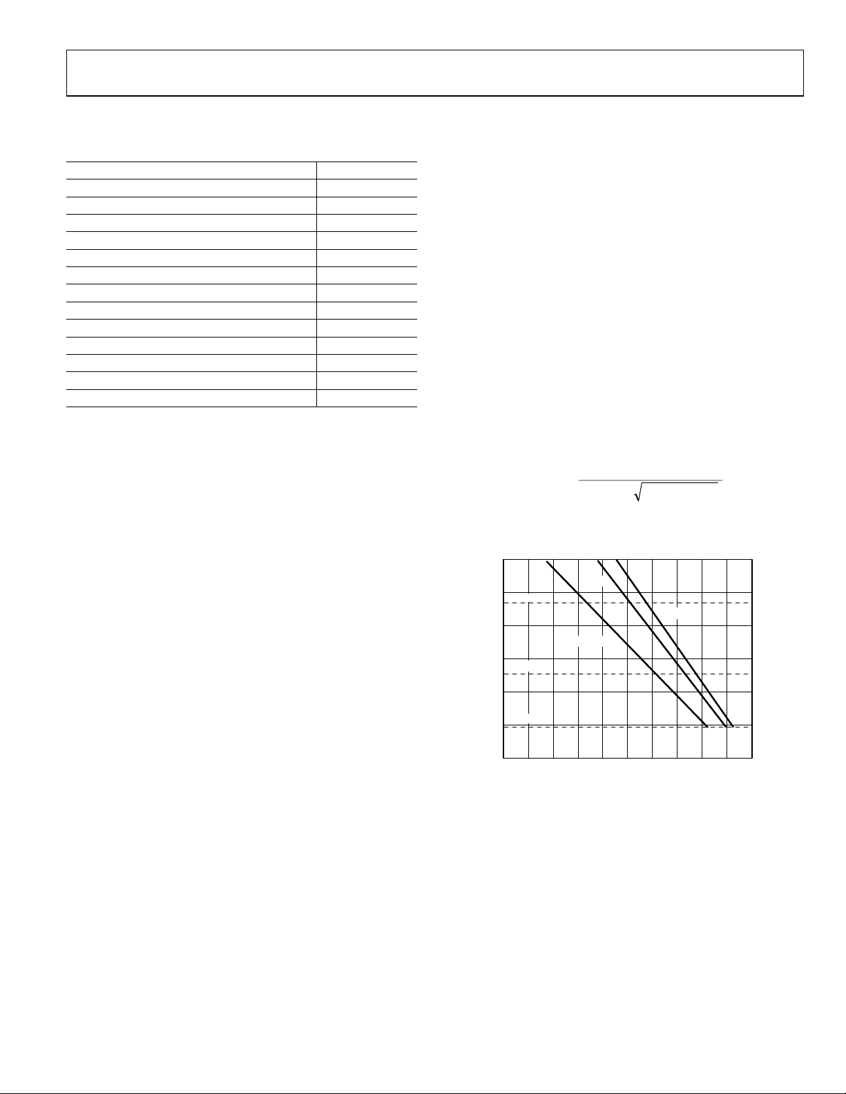
AD8382 ON A 4–LAYER JEDEC PCB WITH THERMALLY OPTIMIZED
LANDING PATTERN AS DESCRIBED IN THE APPLICATION NOTES
2.00
1.75
120MHz
1.50
STILL AIR
1.25
60Hz XGA
1.00
POWER DISSIPATION (W)
Quiescent
0.75
0.50
65 90 95 100 105 11085807570 115
MAXIMUM AMBIENT TEMPERATURE (°C)
Figure 2. Maximum Power Dissipation vs. Temperature.
JA
200 lfm
9.0–(θ
×
A
3
500 lfm
Note: Quiescent power dissipation is 0.74 W when operating
under the conditions specified in this data sheet.
)
lfminAirflow
EXPOSED PADDLE
To ensure a high degree of reliability, the exposed paddle must
be electrically connected to AVCC.
To ensure optimized thermal performance, the exposed paddle
must be thermally connected to the AVCC plane as described in
the Applications section.
Rev. 0 | Page 5 of 24
When driving a 6-channel XGA panel with an input capacitance
of 200 pF, the AD8382 dissipates a total of 1.14 W when
displaying 1 pixel wide alternating white and black vertical lines
generated by a standard 60 Hz XGA input video.
The total power dissipation of the AD8382 is 1.67 W when
operating at the maximum specified frequency of 120 MHz,
under the conditions specified in this data sheet (Figure 2).
Page 6
AD8382
V
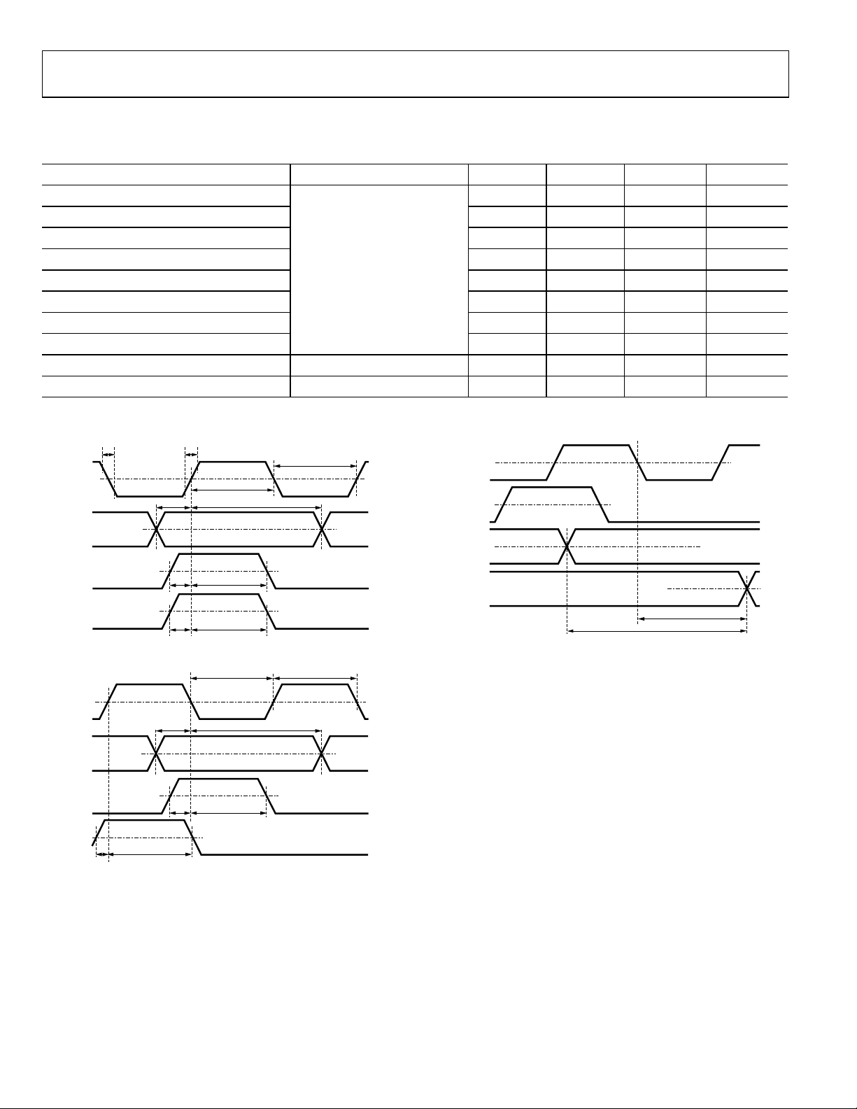
TIMING CHARACTERISTICS
Table 3. Timing Parameters and Conditions
Parameter Conditions Min Typ Max Unit
t1, Data Setup Time 0 ns
t2, Data Hold Time 3 ns
t3, STSQ Setup Time 1 ns
t4, STSQ Hold Time 3 ns
t5, XFR Setup Time 1 ns
t6, XFR Hold Time 3 ns
t7, CLK High Time 3 ns
t8, CLK Low Time
t9, CLK to VIDx Delay To 50% of VIDx 10 12 14 ns
t
INV to VIDx Delay To 50% of VIDx 10.4 12.4 14.4 ns
10,
CLK
DB(0:11)
STSQ
XFR
t
f
Figure 3. Timing Requirement E/O = HIGH
t
r
t
7
t
1
t
3
t
5
t
t
4
t
6
t
8
tr, tf = 2 ns (10% to 90%)
t
8
2
V
TH
V
TH
t
7
2.5 ns
CLK
V
TH
XFR
V
TH
INV
ID(0:5)
V
TH
50%
t
10
Figure 5. Output Timing
V
TH
V
TH
t
9
CLK
DB(0:11)
STSQ
XFR
t
1
t
3
t
5
t
6
t
4
V
TH
Figure 4. Timing Requirement E/O = LOW
t
2
V
TH
V
TH
V
TH
Rev. 0 | Page 6 of 24
Page 7
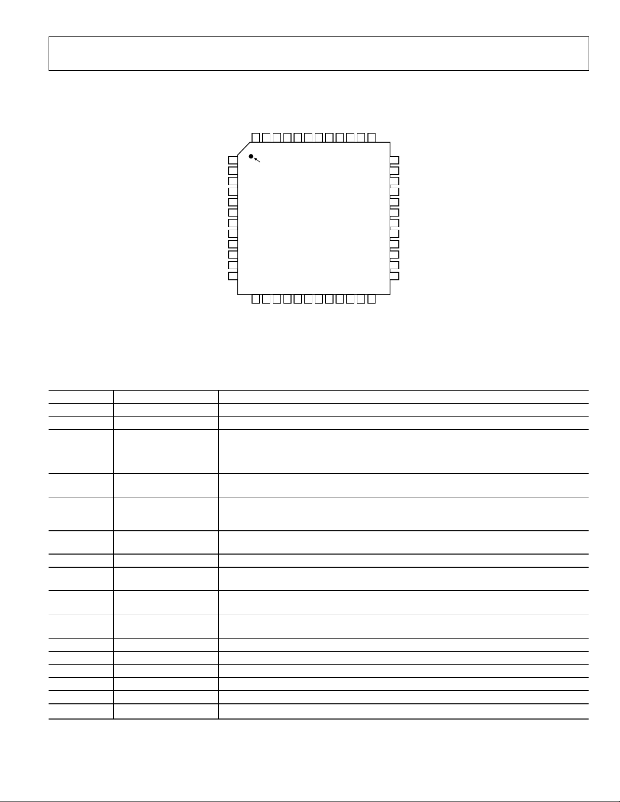
AD8382
A
A
4
PIN CONFIGURATION AND FUNCTIONAL DESCRIPTIONS
CLK
XFR
STSQNCNC
4847464544
V1
AVCCDAC
AGNDDACVREFHI
4342414039
VREFLO
V2
38
AGND0
37
DB0
DB1
DB2
DB3
DB4
DB5
DB6
DB7
DB8
DB9
DB10
DB11
1
PIN 1
INDICATOR
2
3
4
5
6
7
8
9
10
11
12
13
E/O
14
R/L
(Not to Scale)
15
16
INV
DGND
AD8382
TOP VIEW
17
18NC19
DVCC
AVCCBIAS
20
STBY
21
22
BYP
AGNDBIAS
Figure 6. 48-Lead LFCSP, 7 mm × 7 mm Package
36
VID0
35
AVCC0,1
34
VID1
33
GND1,2
32
VID2
31
AVCC2,3
30
VID3
29
GND3,
28
VID4
27
AVCC4,5
VID5
26
25
AGND5
23
24
NC
NC
NC = NO CONNECT
Table 4. Pin Function Descriptions
Mnemonic Function Description
DB(0:11) Data Input 12-Bit Data Input. MSB = DB(11).
CLK Clock Clock Input.
STSQ Start Sequence
R/L Right/Left Select
E/O Even/Odd Select
XFR Data Transfer
VID0–VID5 Analog Outputs These pins are directly connected to the analog inputs of the LCD panel.
V1,V2 Reference Voltages
VREFHI,
Full-Scale References The voltage applied between these pins sets the full-scale output voltage.
VREFLO
INV Invert
DVCC Digital Power Supply Digital Power Supply.
DGND Digital Supply Return This pin is normally connected to the analog ground plane.
AVCCx Analog Power Supplies Analog Power Supplies.
AGNDx Analog Supply Returns Analog Supply Returns.
BYP Bypass A 0.1 µF capacitor connected between this pin and AGND ensures optimum settling time.
STBY Standby When HIGH, the internal circuits are debiased and the power dissipation drops to a minimum.
A new data loading sequence begins on the rising edge of CLK when this input was HIGH on
the preceding rising edge of CLK and the E/O input is held HIGH. A new data loading sequence
begins on the falling edge of CLK when this input was HIGH on the preceding falling edge of
CLK and the E/O input is held LOW.
A new data loading sequence begins on the left, with Channel 0, when this input is LOW, and
on the right, with Channel 5, when this input is HIGH.
The active CLK edge is the rising edge when this input is held HIGH and the falling edge when
this input is held LOW. Data is loaded sequentially on the rising edges of CLK when this input is
HIGH and on the falling edges when this input is LOW.
Data is transferred to the outputs on the immediately following falling edge of CLK when this
input is HIGH on the rising edge of CLK.
The voltages applied between these pins and AGND set the reference levels of the analog
outputs.
When this pin is HIGH, the analog output voltages are at or above V2. When this pin is LOW,
the analog output voltages are at or below V1.
Rev. 0 | Page 7 of 24
Page 8
AD8382
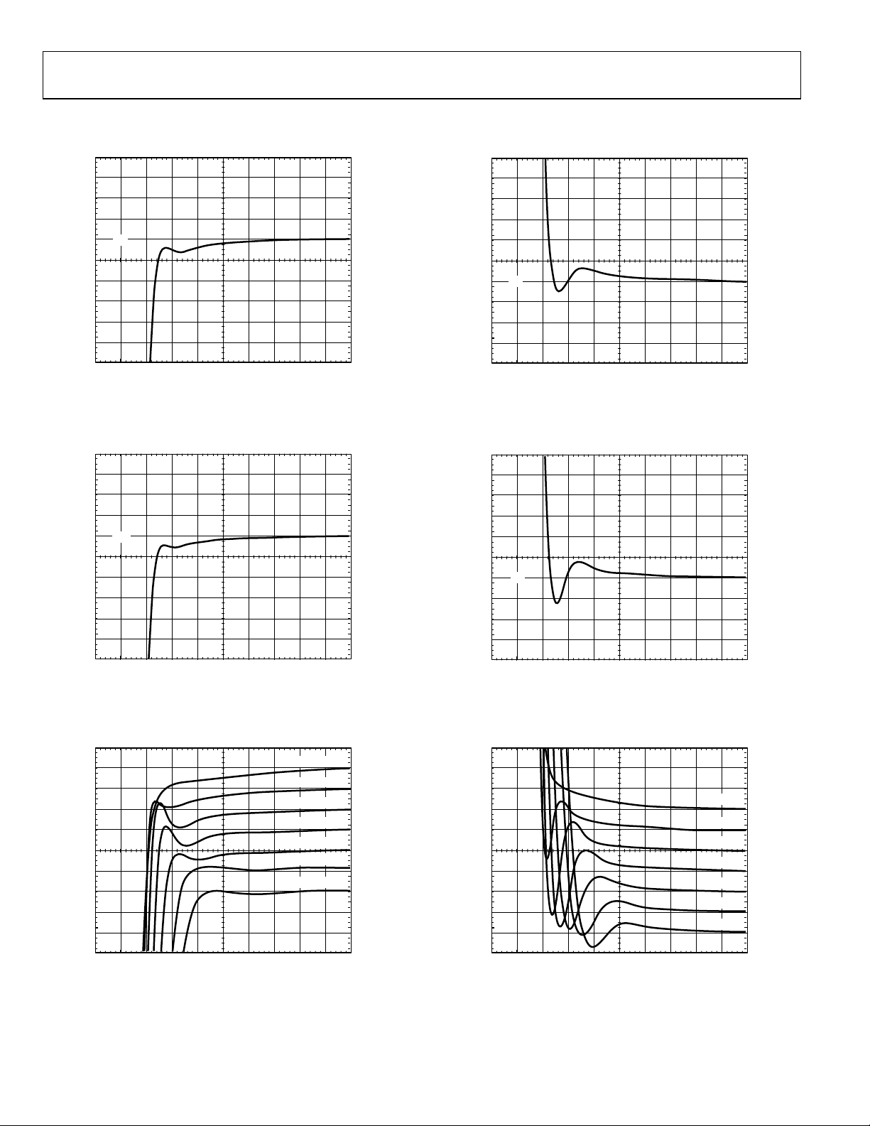
TYPICAL PERFORMANCE CHARACTERISTICS
1.00
0.75
0.50
0.25
0.00
7V
–0.25
–0.50
OUTPUT (%)
–0.75
–1.00
–1.25
–1.50
–20 0 20 40 60 80 100 120 140 160 180
TIME (ns)
Figure 7. Output Settling Time (Rising Edge),
C
= 200 pF, 5 V Step, INV = LOW
L
1.50
1.25
1.00
0.75
0.50
0.25
0.00
OUTPUT (%)
–0.25
–0.50
–0.75
–1.00
2V
–20 0 20 40 60 80 100 120 140 160 180
TIME (ns)
Figure 10. Output Settling Time (Falling Edge),
C
= 200 pF, 5 V Step, INV = LOW
L
1.00
0.75
0.50
0.25
0.00
12V
–0.25
–0.50
OUTPUT (%)
–0.75
–1.00
–1.25
–1.50
–20 0 20 40 60 80 100 120 140 160 180
TIME (ns)
Figure 8. Output Settling Time (Rising Edge),
C
= 200 pF, 5 V Step, INV = HIGH
L
0pF, 12V
47pF, 12V
100pF, 12V
150pF, 12V
200pF, 12V
0.25%/DIV
OUTPUT (%)
250pF, 12V
300pF, 12V
1.50
1.25
1.00
0.75
0.50
0.25
0.00
OUTPUT (%)
–0.25
–0.50
–0.75
–1.00
OUTPUT (%)
7V
–20 0 20 40 60 80 100 120 140 160 180
TIME (ns)
Figure 11. Output Settling Time (Falling Edge),
C
= 200 pF, 5 V Step, INV = HIGH
L
0pF, 7V
47pF, 7V
100pF, 7V
0.25%/DIV
150pF, 7V
200pF, 7V
250pF, 7V
300pF, 7V
–15 0 15 30 45 60 75 90 105 120 135
TIME (ns)
Figure 9. Output Settling Time (Rising Edge) vs. CL,
5 V Step, INV = HIGH
Rev. 0 | Page 8 of 24
–15 0 15 30 45 60 75 90 105 120 135
TIME (ns)
Figure 12. Output Settling Time (Falling Edge) vs. CL,
5 V Step, INV = HIGH
Page 9

AD8382
12
SWITCHING STEP RESPONSE (V)
2
TIME (ns)
Figure 13. Invert Switching Step Response (Rising Edge),
10 V Step, C
7
= 200 pF
L
20ns/DIV
12
SWITCHING STEP RESPONSE (V)
2
Figure 16. Invert Switching Step Response (Falling Edge),
7
TIME (ns)
10 V Step, C
= 200 pF
L
20ns/DIV
2
SWITCHING STEP RESPONSE (V)
TIME (ns)
Figure 14. Data Switching Step Response (Rising Edge),
5 V Step, C
12
7
SWITCHING STEP RESPONSE (V)
=200 pF, INV = LOW
L
TIME (ns)
Figure 15. Data Switching Step Response (Rising Edge),
5 V Step, C
= 200 pF, INV = HIGH
L
20ns/DIV
20ns/DIV
2
SWITCHING STEP RESPONSE (V)
20ns/DIV
Figure 17. Data Switching Step Response (Falling Edge),
5 V Step, C
12
7
SWITCHING STEP RESPONSE (V)
Figure 18. Data Switching Step Response (Falling Edge),
5 V Step, C
TIME (ns)
= 200 pF, INV = LOW
L
TIME (ns)
= 200 pF, INV = HIGH
L
20ns/DIV
Rev. 0 | Page 9 of 24
Page 10

AD8382
2.0
2.0
1.5
1.0
0.5
0
DNL (LSB)
–0.5
–1.0
–1.5
–2.0
0 512 1024 1536 2048 2564 3072 3584 4096
INPUT CODE
Figure 19. Differential Nonlinearity (DNL) vs. Code, INV = LOW
2.0
1.5
1.0
0.5
0
INL (LSB)
–0.5
1.5
1.0
0.5
0
DNL (LSB)
–0.5
–1.0
–1.5
–2.0
0 512 1024 1536 2048 2564 3072 3584 4096
Figure 22. Differential Nonlinearity (DNL) vs. Code, INV = HIGH
2.0
1.5
1.0
0.5
0
INL (LSB)
–0.5
INPUT CODE
–1.0
–1.5
–2.0
0 512 1024 1536 2048 2564 3072 3584 4096
INPUT CODE
Figure 20. Integral Nonlinearity (INL) vs. Code, INV = LOW
3.500
2.625
1.750
0.875
0
VCME (mV)
–0.875
–1.750
–2.625
–3.500
0 512 1024 1536 2048 2564 3072 3584 4096
INPUT CODE
Figure 21. Common-Mode Error Voltage (VCME) vs. Code
–1.0
–1.5
–2.0
0 512 1024 1536 2048 2564 3072 3584 4096
Figure 23. Integral Nonlinearity (INL) vs. Code, INV = HIGH
5.00
3.75
2.50
1.25
0
VDE (mV)
–1.25
–2.50
–3.75
–5.00
0 512 1024 1536 2048 2564 3072 3584 4096
Figure 24. Differential Error Voltage ( VDE) vs. Code
INPUT CODE
INPUT CODE
Rev. 0 | Page 10 of 24
Page 11

AD8382
4
3
2
1
0
–1
–2
NORMALIZED VDE, VCME (mV)
–3
–4
0 1.0 2.0 3.0 4.0 5.0 6.0
VDE
VCME
V2 – V1 (V)
Figure 25. Normalized VDE, VCME vs. (V2 – V1) at Code 2048
10
5
0
NORMALIZED VDE (mV)
–5
4
3
2
1
0
–1
–2
NORMALIZED VDE, VCME (mV)
–3
–4
5.0 6.0 7.0 8.0 9.0 10.0 11.0
Figure 28. Normalized VDE, VCME vs. V1 = V2 at Code 2048
4
3
2
1
0
–1
–2
NORMALIZED VDE, VCME (mV)
–3
VCME
V1 = V2 (V)
V1 = V2 = 5V, VFS = 3V
VDE
VDE
VCME
–10
4 5 6 7 8 9 10 11 12
V2 (V) @ V1 = 7VV1 (V) @ V2 = 7V
Figure 26. Normalized VDE vs. V1 and V2 at Code 2048
3.500
2.625
1.750
0.875
0
VCME (mV)
–0.875
–1.750
–2.625
–3.500
0302010 40 50 60 70 80 90 100
CODE 2048
TEMPERATURE (°C)
Figure 27. Common-Mode Error Voltage (VCME) vs. Temperature
–4
5 6 7 8 9 1011121314
Figure 29. Normalized VDE, VCME vs. VREFLO at Code 2048
5.00
3.75
2.50
1.25
0
VDE (mV)
–1.25
–2.50
–3.75
–5.00
0302010 40 50 60 70 80 90 100
Figure 30. Differential Error Voltage ( VDE) vs. Temperature
VREFLO (V)
CODE 2048
TEMPERATURE (°C)
Rev. 0 | Page 11 of 24
Page 12

AD8382
7.05
V1 = V2 = 7V
7.04
7.03
7.02
7.01
7.00
VID (V)
6.09
6.08
6.07
6.06
6.05
(VID4 – VID5)
VID0, 1, 2, 3
20ns/DIV
5V
VID (V)
7.05
7.04
7.03
7.02
7.01
7.00
6.09
6.08
6.07
6.06
6.05
V1 = V2 = 7V
(VID4 – VID5)
3.3V
DB (0:11)
20ns/DIV
TIME (ns)
Figure 31. All-Hostile Crosstalk at C
800
700
600
500
400
SLEW RATE (V/µs)
300
200
0 50 100 150 200 250 300
10% TO 90%
LOAD CAPACITANCE (pF)
= 200 pF
L
20% TO 80%
Figure 32. Slew Rate vs. CL (Falling Edge)
0
–10
Figure 34. Data Switching Transient (Feedthrough) at C
900
800
700
s)
µ
600
500
SLEW RATE (V/
400
300
200
0 50 100 150 200 250 300
Figure 35. Slew Rate vs. CL (Rising Edge)
TIME (ns)
10% TO 90%
LOAD CAPACITANCE (pF)
= 200 pF
L
20% TO 80%
–20
–30
–40
PSR (dB)
–50
–60
–70
–80
INV = LOW
10k1k10010 100k 1M 10M
FREQUENCY (Hz)
Figure 33. AVCC Power Supply Rejection vs. Frequency
INV = HIGH
Rev. 0 | Page 12 of 24
Page 13

AD8382
V
V
FUNCTIONAL DESCRIPTION
The AD8382 is a system building block designed to directly
drive the columns of LCD microdisplays of the type
popularized for use in projection systems. It comprises six
channels of precision, 12-bit digital-to-analog converters loaded
from a single, high speed, 12-bit wide input. Precision current
feedback amplifiers, providing well-damped pulse response and
fast voltage settling into large capacitive loads, buffer the six
outputs. Laser trimming at the wafer level ensures low absolute
output errors and tight channel-to-channel matching. Tight
part-to-part matching in high resolution systems is guaranteed
by the use of external voltage references.
V1, V2 INPUTS—VOLTAGE REFERENCE INPUTS
Two external analog voltage references set the levels of the
outputs. V1 sets the output voltage at Code 4095 while the INV
input is LOW, and V2 sets the output voltage at Code 4095 while
the INV input is held HIGH.
VREFHI, VREFLO INPUTS—FULL-SCALE REFERENCE INPUTS
Twice the difference between these analog input voltages sets
the full-scale output voltage VFS.
START SEQUENCE CONTROL—INPUT DATA LOADING
A valid STSQ control input initiates a new 6-clock loading
cycle, during which six input data-words are loaded sequentially
into six internal channels. A new loading sequence begins on
the current active CLK edge only when STSQ was held HIGH at
the preceding active CLK edge. Active CLK edge is defined by
the E/O Control.
EVEN/ODD CONTROL—INPUT DATA LOADING
To facilitate 12-channel, single data bus systems, the active CLK
edge, at which input data is loaded, is selected with the E/O
control input. Input data is loaded on the rising CLK edges
while the E/O input is held HIGH; input data is loaded on the
falling CLK edges while the E/O input is held LOW.
RIGHT/LEFT CONTROL—INPUT DATA LOADING
To facilitate image mirroring, the direction of the loading
sequence is set by the R/L control. A new loading sequence
begins at channel 0 and proceeds to Channel 5 when the R/L
control is held LOW. It begins at Channel 5 and proceeds to
channel 0 when the R/L control is held HIGH.
XFR CONTROL—DATA TRANSFER TO OUTPUTS
Data transfer to the outputs is initiated by the XFR control.
While XFR is held HIGH during a rising CLK edge, data is
simultaneously transferred to all outputs on the immediately
following falling CLK edge.
VFS = 2 × (VREFHI – VREFLO)
INV CONTROL—ANALOG OUTPUT INVERSION
The analog voltage equivalent of the input code is subtracted
from (V2 + VFS) while INV is held HIGH and added to (V1 –
VFS) while INV is held LOW.
Transfer Function
The AD8382 has two regions of operation, where the video
output voltages are either above reference voltage V2 or below
reference voltage V1. The transfer function defines the video
output voltage as the function of the digital input code as
follows:
VIDx(n) = V2 + VFS × (1 – n/4095), for INV = HIGH
VIDx(n) = V1 – VFS × (1 – n/4095), for INV = LOW
n = input code
where
VFS = 2 × (VREFHI – VREFLO)
A number of internal limits define the usable range of the video
output voltages, VIDx, as shown in Figure 36
AVCC
2+VFS
V2
VIDx (V)
V1
INV = HIGH
≥ 1.3V
INTERNAL LIMITS AND
USABLE VOLTAGE RANGES
0 ≤ VFS ≤ 5.5V
5V ≤ V2 ≤ (AVCC – 4)
9V ≤ AVCC ≤ 18V
STBY CONTROL—STANDBY MODE
A HIGH applied to the STBY input debiases the internal
circuitry, dropping the quiescent power dissipation to a few
milliwatts. Upon returning STBY to LOW, normal operation is
1–VFS
AGND
restored. Since both analog and digital circuitry is debiased, all
stored data will be lost in standby mode.
Figure 36. Transfer Function and Usable Voltage Ranges
Rev. 0 | Page 13 of 24
INV = LOW
0 4095
INPUT CODE
0 ≤ VFS ≤ 5.5V
5V ≤ V1 ≤ (AVCC – 4)
≥ 1.3V
Page 14

AD8382
Accuracy
To best correlate transfer function errors to image artifacts, the
overall accuracy of the AD8382 is defined by three parameters:
VDE, VCME, and
∆V.
AVCC
(V2 + VFS)
VDE, the differential error voltage, measures the difference
between the rms value of the output and the rms value of the
ideal. The defining expression is:
−−
=
)(
nVDE ×
2
]1)([]2–)([
nVnVOUTPVnVOUTN
1
−−
4095
VCME, the common-mode error voltage, measures one-half the
dc bias of the output. The defining expression is:
++
1
=
)(
nVCME
2
2
)()(
–
)12(
VVnVOUTPnVOUTN
2
∆V measures the maximum deviation between the output
voltages. The defining expression is:
∆V (n) = max{∆VN(n), ∆VP(n)}
where ∆VN(n) = max{VOUTN(n)
and ∆VP(n) = max{VOUTP(n)
(0–5)
} – min{VOUTN(n)
(0–5)
} – min{VOUTP(n)
(0–5)
(0–5)
}
}
VFS
VIDx (V)
(V1 – VF S)
AGND
V2
VOUTN(n)
V1
VOUTP(n)
0 n 4095
INPUT CODE
Figure 37. AD8382 Transfer Function
Rev. 0 | Page 14 of 24
Page 15

AD8382
APPLICATIONS
PIXEL
OPERATING MODES—6-CHANNEL SYSTEMS
Depending on the speed of the LCD microdisplay, 6-channel
systems are compatible with up to XGA resolutions and require
one AD8382 per color. The input/output timing diagram of the
AD8382 in such systems is shown in Figure 38.
DB(0:11)
CLK
STSQ
XFRF
CH 0
CH 1
CH 2
CH 3
CH 4
INTERNAL LATCHESOUTPUTS INPUTS
CH 5
VID0
VID1
VID2
VID3
VID4
VID5
Figure 38. Timing Diagram in a Typical 6-Channel System, E/O=HIGH,
012345678910–1
0
1
2
3
4
–1
–6
–5
–4
–3
–2
–1
6
7
8
5
0
1
2
3
4
5
11 12
9
10
11
6
7
8
9
10
11
R/L=LOW
12
CLK
DB(0:11)
CLK
STSQ
STSQ
XFR
INPUTS
R/L
E/O
EVEN
E/O
ODD
CH 0
CH 1
CH 2
CH 3
CH 4
INTERNAL LATCHESOUTPUTS
CH 5
VID0
VID1
AD8382 EVENAD8382 ODD
VID2
VID3
VID4
VID5
–2–1012345678–3 9 10 121314151617181920212211 23 24
0
2
4
6
–2
–12
–10
–8
–6
–4
–2
12
14
16
18
8
10
0
2
4
6
8
10
20
22
12
14
16
18
20
22
OPERATING MODES—12-CHANNEL SYSTEMS
12-channel systems are usually those requiring video line
doubling or compatibility with SXGA and higher resolutions.
Depending on the input data rates, two types of 12-channel
systems are in common use.
12-Channel, Even/Odd Systems
Single data bus systems are characterized by an image processor
with a single data bus output. They require two AD8382s per
color.
One AD8382 is set to operate in EVEN mode, while the other is
set to operate in ODD mode. Both AD8382s share the same
data bus and CLK. The timing diagram of such a system is
shown in Figure 39.
12-Channel Parallel Systems
Dual data bus systems are characterized by an image processor
with two data bus outputs. They require two AD8382s per color.
Both AD8382s in dual data bus systems can be set
independently. The timing diagram of each AD8382 in such
systems is identical to that of a 6-channel system.
CH 0
CH 1
CH 2
CH 3
CH 4
INTERNAL LATCHESOUTPUTS
CH 5
VID0
VID1
VID2
VID3
VID4
VID5
1
3
5
7
9–3
–1
–11
–9
–7
–5
–3
–1
13
15
17
19
21
11
1
3
5
7
9
11
23
13
15
17
19
21
23
Figure 39. 12-Channel Even/Odd System Timing Diagram
OPERATING MODES—BEYOND 12 CHANNELS
Any number of AD8382s may be cascaded in even/odd pairs or
in parallel to facilitate very high resolution systems.
Rev. 0 | Page 15 of 24
Page 16

AD8382
H. REVERSE
HSYNC
VSYNC
H. REVERSE
HSYNC
VSYNC
STSQ2
STSQ1
CLK
CLK
CLK
CLK
D(0:9) Odd
D(0:9) Even
CLK
D(0:9) Even
D(0:9) Odd
IMAGE PROCESSOR
Pixel CLK
÷6 COUNTER
÷6 COUNTER
HSTART
INV1
INV2
IMAGE PROCESSOR
Pixel CLK
÷6 COUNTER
HSTART
INV1
INV2
DB1(0:11)
CLK
÷2
XFR
R/L
STSQ1
INV1
E/O1
STSQ2
INV2
E/O2
REFERENCES
VREFHI
VREFLO
V2
V1
Figure 40. Single Data Bus 12-Channel Even/Odd System Block Diagram
DB1(0:11)
CLK
÷2
XFR
R/L
STSQ
INV1
“1”
E/O
INV2
DB2(0:11)
REFERENCES
VREFHI
VREFLO
V2
V1
Figure 41. Dual Data Bus 12-Channel Even/Odd System Block Diagram
DB(0:11)
CLK
XFR
R/L
STSQ
INV
E/O
VREFHI
VREFLO
V2
V1
DB(0:11)
CLK
XFR
R/L
STSQ
INV
E/O
VREFHI
VREFLO
V2
V1
DB(0:11)
CLK
XFR
R/L
STSQ
INV
E/O
VREFHI
VREFLO
V2
V1
DB(0:11)
CLK
XFR
R/L
STSQ
INV
E/O
VREFHI
VREFLO
V2
V1
AD8382
VID0
VID1
VID2
VID3
VID4
VID5
AD8382
VID0
VID1
VID2
VID3
VID4
VID5
AD8382
VID0
VID1
VID2
VID3
VID4
VID5
AD8382
VID0
VID1
VID2
VID3
VID4
VID5
Ch 0
Ch 2
Ch 4
Ch 6
Ch 8
Ch 10
12 – CHANNEL
LCD
CH 1
CH 3
CH 5
CH 7
CH 9
CH 11
Ch 0
Ch 2
Ch 4
Ch 6
Ch 8
Ch 10
12 – CHANNEL
LCD
CH 1
CH 3
CH 5
CH 7
CH 9
CH 11
Rev. 0 | Page 16 of 24
Page 17

AD8382
V
V
VBIAS Generation—V1, V2 Input Pin Functionality
In order to avoid image flicker, a symmetrical ac voltage is
required and a bias voltage of approximately 1 V minimum
must be maintained across the pixels of HTPS LCDs. The
AD8382 provides two methods of maintaining this bias voltage.
INTERNAL BIAS VOLTAGE GENERATION
Standard systems that internally generate the bias voltage
reserve the uppermost code range for the bias voltage and use
the remaining code range to encode the video for gamma
correction. A high degree of ac symmetry is guaranteed by the
AD8382 in these systems.
The V1 and V2 inputs in these systems are tied together and are
normally connected to VCOM, as shown in Figure 42.
VFS = 5V
AD8382
VCOM
V2
V1
VCOM
Figure 42. V1, V2 Connection and Transfer Function in a Typical Standard
System
EXTERNAL BIAS VOLTAGE GENERATION
In systems that require improved brightness resolution and
higher accuracy, the V1 and V2 inputs, connected to external
voltage references, provide necessary bias voltage, VBIAS, while
allowing the full code range to be used for gamma correction.
To ensure a symmetrical ac voltage at the AD8382’s outputs,
VBIAS must remain constant for both states of INV. Thus, V1
and V2 are defined as:
V1 = VCOM − VBIAS
V2 = VCOM + VBIAS
VBIAS = 1V
VBIAS = 1V
VFS = 5V
40953280
RESERVED
CODE
RANGE
APPLICATIONS CIRCUIT
The circuit in Figure 41 ensures VBIAS symmetry to within 1
mV with a minimum component count. Bypass capacitors are
omitted for clarity.
AVCC = 15.5V
VZ = 5.1V
–IN
V+
VCOM
AD8132
V–
+IN
DVCC = 3.3V
3
5
4
6
V2 = 8V
V1 = 6V
COM = 7V
R2 = 1kΩ
R1 = 6kΩ
1
2
8
Figure 43. External VBIAS Generator with the AD8132
VFS = 4V
V2
COM
V1
VBIAS = 1V
VBIAS = 1V
VFS = 4V
Figure 44. The AD8382 Transfer Function in a Typical High Accuracy System
8.75
7.50
6.25
5.00
3.75
2.50
1.25
0.00
–1.25
–2.50
–3.75
(V2 + V1)/2 – VCOM (mV)
–5.00
–6.25
–7.50
–8.75
5.7 6.2 6.7 7.2 7.7 8.2 8.7 9.2 9.7 10.2 10.7
TA = 85°C
+
V
– V– (V)
Figure 45. Typical Asymmetry at the Outputs of the AD8132 vs. Power Supply
for the Application Circuit
The AD8132 typically produces a symmetrical output at 85°C
when its supply, (V+) – (V–), is 7.2 V (Figure 45).
AD8382
V2
V1
4095
TA = 25°C
Rev. 0 | Page 17 of 24
Page 18

AD8382
Power Supply Sequencing
As indicated in the Absolute Maximum Ratings, voltage at any
input pin cannot exceed its supply voltage by more than 0.5 V.
To ensure compliance with these ratings, the following powerup and power-down sequencing is recommended.
During power-up, initial application of nonzero voltages to any
input pin must be delayed until supply voltage ramps up to at
least the highest maximum operational input voltage. During
power-down, the voltage at any input pin must reach zero
during a period not exceeding the power supply’s hold-up time.
Failure to comply with the Absolute Maximum Ratings may
result in functional failure or damage to the internal ESD
diodes. Damaged ESD diodes may cause temporary parametric
failures, which may result in image artifacts. Damaged ESD
diodes cannot provide full ESD protection, reducing reliability.
Power ON Power OF F
The AD8382 package is designed to provide superior thermal
characteristics, partly through the exposed die paddle on the
bottom surface of the package. In order to take full advantage of
this feature, the exposed paddle must be in direct thermal
contact with the PCB, which then serves as a heat sink.
Table 5. AD8382 Power Dissipation
V
= 5 V V
QUIESCENT
(W)
C
LOAD
(pF)
200 0.74 0.93 1.67 0.74 1.48
250 0.74 1.16 1.90 0.93 1.67
300 0.74 1.39 2.13 1.11 1.85
P
P
DYNAMIC
(W)
SWING
P
TOTAL
(W)
P
DYNAMIC
(W)
SWING
= 4 V
P
(W)
TOTAL
A thermally effective PCB must incorporate a thermal pad and
a thermal via structure. The thermal pad provides a solderable
contact surface on the top surface of the PCB. The thermal via
structure provides a thermal path to the inner and bottom
layers of the PCB to remove heat.
1. Apply power to supplies. 1. Remove power from I/Os.
2. Apply power to other I/Os. 2. Remove power from
supplies.
PCB Design for Optimized Thermal Performance
The total maximum power dissipation of the AD8382 is partly
load dependent. In a 6-channel, 65 MHz, 60 Hz XGA system,
the total maximum power dissipation is 1.14 W at an LCD input
capacitance of 200 pF.
At a clock rate of 120 Ms/s, the total maximum power
dissipation can exceed 2 W, as shown below for a black-to-white
video output voltage swing of 4 V and 5 V.
Although the maximum safe operating junction temperature is
higher, the AD8382 is 100% tested at a junction temperature of
125°C. Consequently, the maximum guaranteed operating
junction temperature is 125°C. To limit the maximum junction
temperature at or below the guaranteed maximum, the package,
in conjunction with the PCB, must effectively conduct heat
away from the junction.
THERMAL PAD DESIGN
Thermal performance of the AD8382 varies logarithmically
with the contact area between the exposed thermal paddle and
the thermal pad on the top layer of the PCB.
In order to minimize thermal performance degradation of
production PCBs, the contact area between the thermal pad and
the PCB should be maximized. Therefore, the size of the
thermal pad should match the exposed paddle size of 5.25 mm
× 5.25 mm. In addition, a second thermal pad of the same size
should be placed on the bottom side of the PCB. At least one
thermal pad should be in direct thermal (and electrical) contact
with the AVCC plane.
THERMAL VIA STRUCTURE DESIGN
Effective heat transfer from the top to the inner and bottom
layers of the PCB requires thermal vias incorporated into the
thermal pad design. Thermal performance increases
logarithmically with the number of vias. θ
value at approximately 16 vias, provided the AD8382 is on a
standard JEDEC PCB. θ
approaches its optimum value as the
JA
slope of such a curve approaches zero, at above 36 vias. Near
optimum thermal performance of production PCBs is attained
when the number of thermal vias is at least 36.
reaches its specified
JA
Rev. 0 | Page 18 of 24
Page 19

AD8382
AD8382 PCB DESIGN RECOMMENDATIONS
Land pattern Dimensions
Pad Size:
0.5 mm × 0.25 mm
Pad Pitch:
0.5 mm
Thermal Pad Size:
5.25 mm × 5.25 mm
Thermal via structure:
0.25 mm diameter.
Vias on 0.5mm grid.
7mm
Figure 46. Land Pattern—Top Layer
7mm
LAND PATTERN – TOP LAYER
THERMAL PAD AND VIA CONNECTIONS
Thermal Pads are connected to AVCC.
For PCBs with the AVCC
plane located on one of
the outer layers, direct
connection of at least one
thermal pad to the AVCC
plane is recommended.
For PCBs with the AVCC
plane located on one of
the internal layers, direct
connection of all thermal
vias to the AVCC plane is
recommended.
The use of thermal spokes is not recommended when
connecting the thermal pads or via structure to the AVCC
plane.
LAND PATTERN – BOTTOM LAYER
Figure 47. Land Pattern—Bottom Layer
SOLDER MASKING
To minimize the formation of solder voids due to solder flowing
into the via holes (solder wicking), via diameter should be small.
Solder masking of the via holes on the top layer of the PCB
plugs the via holes, inhibiting solder flow into the holes. To
optimize the thermal pad coverage, the solder mask diameter
should be no more than 0.1 mm larger than the via diameter.
Solder Mask—Top Layer
Pads: Set by customer’s PCB
Design Rules
Thermal Vias: 0.25 mm dia.
circular mask, centered on the
vias.
Solder Mask—Bottom
Layer
Set by customer’s PCB Design
Rules.
SOLDER MASK – TOP LAYER
Figure 48. Solder Mask—Top Layer
Rev. 0 | Page 19 of 24
Page 20

AD8382
Layout Considerations
The AD8382 is a mixed-signal, high speed, high accuracy
device. In order to fully realize its specifications, it is essential to
use a properly designed printed circuit board.
LAYOUT AND GROUNDING
The analog outputs and the digital inputs of the AD8382 are on
opposite sides of the package. Keep these sections separated to
minimize crosstalk and coupling of digital inputs into the
analog outputs.
All signal trace lengths should be made as short and direct as
possible to prevent signal degradation due to parasitic effects.
Note that digital signals should not cross and should not be
routed near analog signals.
It is imperative to provide a solid analog ground plane under
and around the AD8382. All ground pins of the part should be
connected directly to this ground plane with no extra signal
path length. This includes DGND, AGNDBIAS, AGND5,
AGND3,4, AGND1,2, AGND0, and AGNDDAC. The return
traces for any of the signals should be routed close to the
ground pin for that section to prevent stray signals from
coupling into other ground pins.
POWER SUPPLY BYPASSING
All power supply and reference pins of the AD8382 must be
properly bypassed to the analog ground plane for optimum
performance.
All analog supply pins may be connected directly to an analog
supply plane located as close to the part as possible. A 0.1 µF
chip capacitor should be placed as close to each analog supply
pin as possible and connected directly between each analog
supply pin and the analog ground plane.
A minimum 47 µF tantalum capacitor should be placed near the
analog supply plane and connected directly between the supply
and analog ground planes.
A minimum 10 µF tantalum capacitor should be placed near the
digital supply pin and connected directly to the analog ground
plane. A 0.1 µF chip capacitor should be connected between the
digital supply pin and the analog ground.
VREFHI, VREFLO, V2, V1 REFERENCE DISTRIBUTION
To ensure well-matched video outputs, all AD8382s must
operate from equal reference voltages.
Each reference voltage should be distributed to each AD8382
directly from the source of the reference voltage with
approximately equal trace lengths.
A 0.1 µF chip capacitor should be placed as close to each
reference input pin as possible and directly connected between
the reference input pin and the analog ground plane.
Rev. 0 | Page 20 of 24
Page 21

AD8382
OUTLINE DIMENSIONS
0.30
0.23
0.18
PIN 1
48
INDICATOR
1
BSC SQ
PIN 1
INDICATOR
7.00
0.60 MAX
37
36
0.60 MAX
5.25
SQ
5.10
4.95
12
13
1.00
0.90
0.80
0.20
REF
12° MAX
SEATING
PLANE
TOP
VIEW
0.80 MAX
0.65 NOM
0.50 BSC
COMPLIANT TO JEDEC STANDARDS MO-220-VKKD-2
6.75
BSC SQ
0.50
0.40
0.30
0.05 MAX
0.02 NOM
COPLANARITY
0.08
25
BOTTOM
VIEW
24
5.50
REF
Figure 49. 48-Lead Frame Chip Scale Package [LFCSP] (CP-48)—Dimensions shown in millimeters
ESD CAUTION
ESD (electrostatic discharge) sensitive device. Electrostatic charges as high as 4000 V readily accumulate on the
human body and test equipment and can discharge without detection. Although the AD8382 features
proprietary ESD protection circuitry, permanent damage may occur on devices subjected to high energy
electrostatic discharges. Therefore, proper ESD precautions are recommended to avoid performance
degradation or loss of functionality.
Ordering Guide
Table 6.
Model Temperature Range Package Description Package Option
AD8382ACP 0°C to 85°C 48-Lead LFCSP CP-48
Rev. 0 | Page 21 of 24
Page 22

AD8382
Rev. 0 | Page 22 of 24
Page 23

AD8382
Rev. 0 | Page 23 of 24
Page 24

AD8382
© 2003 Analog Devices, Inc. All rights reserved. Trademarks and
registered trademarks are the property of their respective companies.
Printed in the U.S.A.
C03371-0-2/03(0)
Rev. 0 | Page 24 of 24
 Loading...