

Page 1
Fast, High-Voltage Drive, 6-Channel Output
a
DecDriver™ Decimating LCD Panel Driver
FEATURES
High-Voltage Drive to Within 1.3 V of Supply Rails
24 V Supply for Fast Output Voltage Drivers
High Update Rates: Fast 75 Ms/s 10-Bit Input Word Rate
Low Power Dissipation, 550 mW with Power-Down
Voltage Controlled Video Reference and Full-Scale
(Contrast) Output Levels
INV Bit Reverses Polarity of Video Signal
Nominal 3.3 V Logic and 15 V Analog Supplies
Flexible Logic
Addressable or Sequential Channel Loading
STSQ/CS Allow Parallel AD8380 Operation for XGA
and Greater Resolution
Drives Capacitive Loads
26 ns Settling Time to 1% Up to 150 pF Load
Slew Rate 270 V/s
Available in 44-Lead MQFP
APPLICATIONS
Poly Si LCD Panel Analog Column Driver
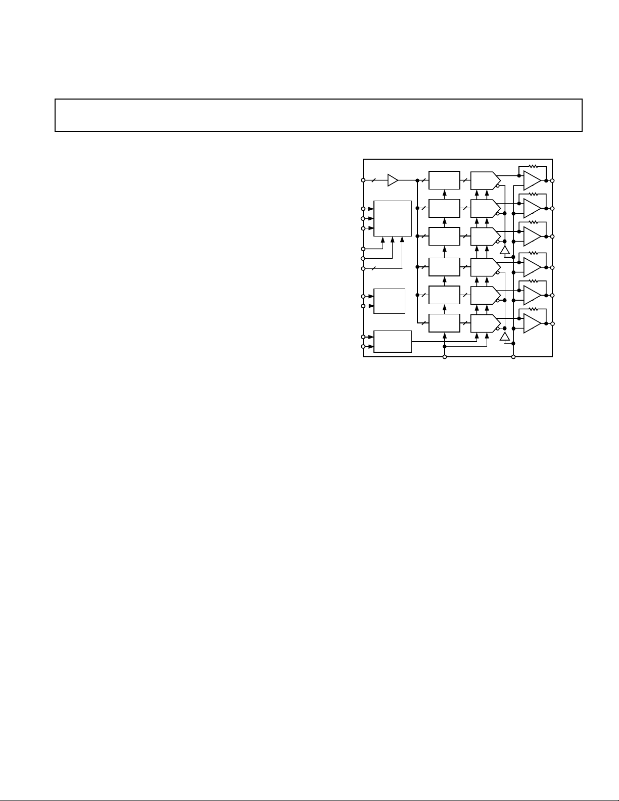
DB [0:9]
CLK
STSQ/CS
XFR
E/O
R/L
A[0:2]
STBY
BYP
VREFHI
VREFLO
AD8380
FUNCTIONAL BLOCK DIAGRAM
10
CHANNEL
SELECTOR
3
BIAS
SCALING
CONTROL
AD8380
10
10
10
10
10
1010
2-STAGE
LATCH
2-STAGE
LATCH
2-STAGE
LATCH
2-STAGE
LATCH
2-STAGE
LATCH
2-STAGE
LATCH
INV VMID
DAC
10
DAC
10
DAC
10
DAC
10
DAC
10
DAC
VID0
VID1
VID2
VID3
VID4
VID5
PRODUCT DESCRIPTION
The AD8380 provides a fast, 10-bit latched decimating digital
input that drives 6-channel high voltage drive outputs. The 10bit input word is sequentially muxed into six separate high speed,
bipolar DACs. Flexible digital input formats allow several
AD8380s to be used in parallel for higher resolution displays.
STSQ/CS, in conjunction with 3-bit addressable channel-loading
pins, allows loading of the digital words either sequentially or
randomly, and R/L control sets loading as either left to right, or
vice versa. 6-channel high voltage output drivers drive to within
1.3 V of the rails to rated settling time. The output signal can be
adjusted for dc signal reference, signal inversion or contrast for
maximum flexibility.
The AD8380 is fabricated on ADI’s XFCB26 fast bipolar 26 V
process, providing fast input logic, trimmed accuracy bipolar
DACs and fast settling, high voltage precision drive amplifiers
on the same chip.
The AD8380 dissipates nominally 0.55 W of static power. STBY
pin reduces power to a minimum, with fast recovery.
The AD8380 is offered in a 44-lead 10 × 10 × 2.0 mm MQFP
package and operates over the commercial temperature range of
0°C to 85°C.
DecDriver is a trademark of Analog Devices, Inc.
REV. B
Information furnished by Analog Devices is believed to be accurate and
reliable. However, no responsibility is assumed by Analog Devices for its
use, nor for any infringements of patents or other rights of third parties that
may result from its use. No license is granted by implication or otherwise
under any patent or patent rights of Analog Devices.
One Technology Way, P.O. Box 9106, Norwood, MA 02062-9106, U.S.A.
Tel: 781/329-4700 www.analog.com
Fax: 781/326-8703 © Analog Devices, Inc., 2001
Page 2

AD8380–SPECIFICATIONS
(@ 25ⴗC, AVCC = 15 V, DVCC = 3.3 V, T
otherwise noted)
= 0ⴗC, T
MIN
= 85ⴗC, unless
MAX
Model Conditions Min Typ Max Unit
VIDEO DC PERFORMANCE
1
T
to T
MIN
MAX
VDE DAC Code = 450 to 800 –7.5 +1 +7.5 mV
VCME DAC Code = 450 to 800 –3.5 +0.5 +3.5 mV
Scale Factor Error DAC Code = 0 to 1023 –0.25 +0.25 %
Offset Error DAC Code = 0 to 1023 –7 +1 +7 mV
REFERENCE INPUTS
VMID Range
2
6 7 7.5 V
VMID Bias Current 3 µA
VFS Range VFS = 2 × (VREFHI–VREFLO) 1 5 6 V
VREFHI VREFLO +0.5 AVCC – 2.5 AVCC V
VREFLO VMID – 0.5 VREFHI – 2.5 VREFHI – 0.5 V
VREFHI Input Resistance to VREFLO 3.3 kΩ
VREFLO Bias Current 0.2 µA
VREFHI Input Current
3
VFS = 5 V 750 µA
RESOLUTION
Coding Binary 10 Bits
DIGITAL INPUT CHARACTERISTICS
Input Data Update Rate 75 Ms/s
Clock to Data Setup Times: t
Clock to STSQ Setup Times: t
Clock to XFR Setup Times: t
1
3
5
Maximum CLK Rise and Fall Time, t
Clock to A[0:2] Hold Times: t
Clock to Data Hold Times: t
Clock to STSQ Hold Times: t
Clock to XFR Hold Times: t
Clock to A[0:2] Setup Times: t
C
IN
I
IN
V
IH
V
IL
V
TH
9
2
4
6
8
7
Threshold Voltage 1.4 V
1ns
1ns
1ns
4ns
4ns
4ns
4ns
4ns
1ns
3pF
0.6 µA
2.0 V
0.8 V
VIDEO OUTPUT CHARACTERISTICS
Output Voltage Swing AVCC – VOH, VOL – AVEE 1.1 1.3 V
CLK to VID Delay
4
50% of VIDx 13.5 15.5 17.5 ns
Output Current 30 mA
VIDEO OUTPUT DYNAMIC PERFORMANCE T
MIN
to T
MAX
, VO = 5 V Step,
CL = 150 pF, RS = 25 Ω
Data Switching Slew Rate 270 V/µs
Invert Switching Slew Rate 625 V/µs
Data Switching Settling Time to 1%
Data Switching Settling Time to 0.25% 35 65 ns
Invert Switching Settling Time to 1%
Invert Switching Settling Time to 0.25% 85 100 ns
CLK Feedthrough
All-Hostile Crosstalk
6
7
5
5
26 32 ns
30 40 ns
2 5 mV p-p
Amplitude 95 mV p-p
Glitch Duration 40 ns
POWER SUPPLY
Supply Rejection (VDE) +VS = 15 V ± 1 V 1 mV/V
DVCC, Operating Range 3 5.5 V
DVCC, Quiescent Current 22 35 mA
AVCC, Operating Range 9 24 V
Total AVCC Quiescent Current 33 44 mA
STBY AVCC Current STBY = H 0.5 5 mA
STBY DVCC Current STBY = H 0.1 5 mA
OPERATING TEMPERATURE RANGE 0 85 °C
NOTES
1
For definitions of VDE and VCME, see the Transfer Function section. Scale factor error is expressed as percentage of VFS.
2
See Figure 1 for valid ranges of VMID.
3
VREFHI Input Current = (VREFHI – VREFLO)/(VREFHI Input Resistance) = 2.5 V/3.3 kΩ.
4
Delay time from 50% of falling CLK edge to 50% of output change. Measurement is made for both states of INV.
5
For best settling time results, use minimum series output resistance, RS of 25 Ω.
6
An output channel is selected, and glitch is monitored as CLK is driven. STSQ and XFR are set to logic low.
7
Input data is loaded such that any five output channels change by VFS (i.e., 5 V), and the sixth unselected channel is monitored. Measurement is made for both states of INV.
Specifications subject to change without notice.
–2–
REV. B
Page 3
AD8380
VFS – Volts
6 7.5
VMID – Volts
6
4.5
PIN FUNCTION DESCRIPTIONS
Pin No. Mnemonic Description
1 NC No Connect.
2–11 DB[0:9] Video Data Inputs. DB9 is the MSB.
12 E/O Even/Odd data select, input latches are loaded at the falling edge of CLK if E/O is low or
rising edge if E/O is high.
13 R/L Determines starting point of internally generated channel-loading sequence.
R/L Low (when address = 111) loads from Channel 0 up to Channel 5.
14 INV When high, analog video outputs are above the VMID setpoint. See Figure 3.
15, 16 DVEE, DVCC Digital Supplies. Nominally 3.3 V and 0 V, respectively.
17, 20, 22, 24,
26, 28, 30, 32,
34, 37, 38 AVCCxxx, AVEExxx Analog Supplies. Nominally 15 V and 0 V, respectively.
18 STBY Stand By. When high, all digital and analog circuits are “debiased” and the power dissipation
drops to a minimum.
19 BYP An external capacitor connected from here to V
21 VMID Externally supplied voltage applied here sets the midpoint reference for the video output.
23, 25, 27, 29,
31, 33 VID5–VID0 Analog Video Outputs.
36, 35 VREFHI, VREFLO Voltage between these pins sets DAC full-scale range. An external reference must be applied
and should be common to all devices to ensure best tracking.
39–41 A[0:2] 3-bit channel address for addressable loading of the digital input latches.
42 STSQ/CS STSQ to start internal sequencing or Chip Select to enable addressable channel addressing.
See functional description. Used in conjunction with A[0:2].
43 XFR If XFR = HIGH at the rising edge of CLK, data is transferred to the DACs on the next falling
edge of CLK. See Figures 4, 6, 7, and 8.
44 CLK Master Clock Input.
will help to ensure rapid DAC settling time.
EE
CHANNEL SELECTION FUNCTIONALITY
There are two channel selection modes, addressed channel
loading, (in which the user directly controls which DAC is
loaded), and internally sequenced loading (in which the user
controls the direction and clock phase in which the loading
proceeds).
ADDRESSED CHANNEL LOADING:
When channel address (A0, A1, A2) = 000 through 101, the
video data is loaded into Channels 0 through 5. (STSQ/CS
functions as “Chip Selection” this case.)
INTERNALLY SEQUENCED LOADING:
When channel address = 111 the video data is loaded in a
sequence determined internally. The sequencing is initiated by
a pulse applied to STSQ/CS input. The count proceeds from
0 to 5 if R/L is LOW or from 5 to 0 if R/L is HIGH.
DAC TRANSFER FUNCTION
V
= VMID + VFS × (1 – N/1023); if INV is HIGH,
OUT
= VMID – VFS × (1 – N/1023); if INV is LOW
V
OUT
where VFS = 2 × (VREFHI – VREFLO)
MAXIMUM OUTPUT VOLTAGE
The maximum output signal swing is constrained by the output
voltage compliance of the DACs and the output dynamic range
of the output amplifiers. The minimum voltage allowed at the
outputs of the DACs is about 6 V. This constrains the minimum
value of VMID to be 6 V. The output amplifiers will swing and
settle cleanly, as described on the specification page, for output
voltages within 1.5 V from each supply voltage rail.
For a given value of V
, the voltage required to saturate the
MID
video output voltages defines the maximum usable full-scale
voltage. For example, if VMID is less than AVCC/2, the maximum value of VFS is (VMID – 1.5 V). If VMID is greater than
AVCC/2, the maximum useful VFS is (AVCC – 1.5 – VMID).
Figure 1 graphically describes these limiting factors.
Figure 1. Valid Range for VMID with Respect to VFS
(AVCC = 15 V)
REV. B
–3–
Page 4
AD8380
ABSOLUTE MAXIMUM RATINGS
Supply Voltage AVCC–AVEE . . . . . . . . . . . . . . . . . . . . . 26 V
Internal Power Dissipation
2
1
Quad Flat Package (S) . . . . . . . . . . . . . . . . . . . . . . . 1.7 W
Output Short Circuit Duration
. . . . . . . . . . . . . . . . . . . . . . . . . . . . . . See Associated Text
Storage Temperature Range . . . . . . . . . . . . –65°C to +125°C
Operating Temperature Range . . . . . . . . . . . . . . 0°C to 85°C
Lead Temperature Range (Soldering 10 sec) . . . . . . . . . 300°C
NOTES
1
Stresses above those listed under Absolute Maximum Ratings may cause perma-
nent damage to the device. This is a stress rating only; functional operation of the
device at these or any other conditions above those indicated in the operational
section of this specification is not implied. Exposure to absolute maximum rating
conditions for extended periods may affect device reliability.
2
Specification is for device in free air:
44-Lead MQFP Package: θJA = 73°C/W (Still Air), where PD = (TJ – TA)/θJA.
θJC = 22°C/W.
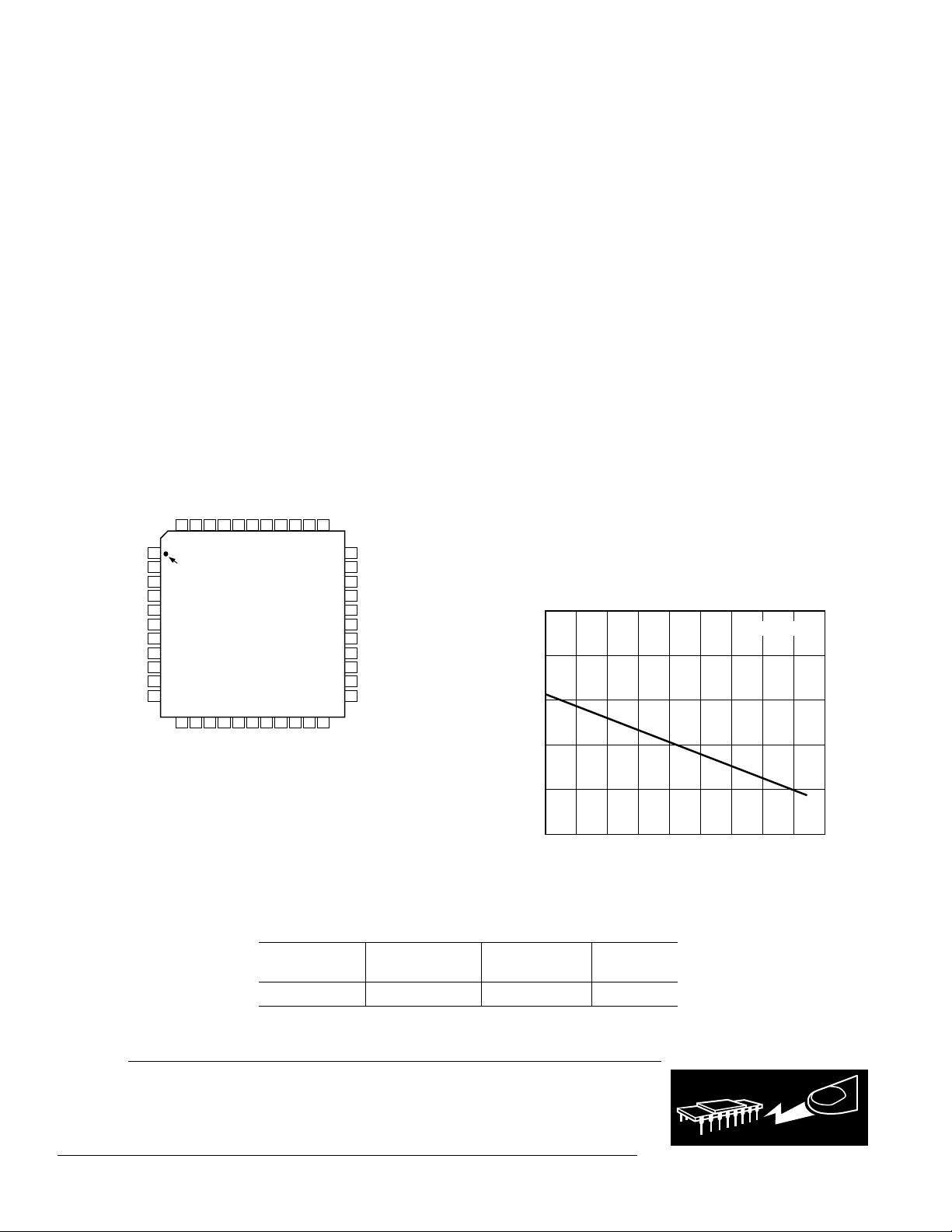
PIN CONFIGURATION
CLK
XFR
1
NC
2
DB0
3
DB1
4
DB2
5
DB3
6
DB4
7
DB5
8
DB6
9
DB7
10
DB8
(MSB) DB9
NC = NO CONNECT
11
STSQ/CSA0A1A2AVCCDAC
44 43 42 41 40 39 38 37 36 35 34
PIN 1
IDENTIFIER
AD8380
TOP VIEW
(Not to Scale)
12 13 14 15 16 17 18 19 20 21 22
INV
R/L
E/O
DVEE
DVCC
AVCC BIAS
AVEEDAC
BYP
STBY
VREFHI
VREFLO
AVEE0
VMID
AVEE5
AVEE BIAS
33
32
31
30
29
28
27
26
25
24
23
VID0
AVCC0,1
VID1
AVEE1,2
VID2
AVCC2,3
VID3
AVEE3,4
VID4
AVCC4,5
VID5
MAXIMUM POWER DISSIPATION
The maximum power that can be safely dissipated by the
AD8380 is limited by the associated rise in junction temperature.
The maximum safe junction temperature for plastic encapsulated
devices is determined by the glass transition temperature of the
plastic, approximately 150°C. Exceeding this limit temporarily
may cause a shift in parametric performance due to a change in
the stresses exerted on the die by the package. Exceeding a junction temperature of 175°C for an extended period can result in
device failure.
Output Short Circuit Limit
The AD8380’s internal short circuit limitation is not sufficient to
protect the device in the event of a direct short circuit between a
video output and a power supply voltage rail (V
or VEE). Tem-
CC
porary short circuits can reduce an output’s ability to source or
sink current and, therefore, impact the device’s ability to drive a
load. Short circuits of extended duration can cause metal lines to
fuse open, rendering the device nonfunctional.
To prevent these problems, it is recommended that a series
resistor of 25 Ω or greater be placed as close as possible to the
AD8380’s video outputs. This will serve to substantially reduce
the magnitude of the fault currents and protect the outputs from
damage caused by intermittent short circuits. This may not be
enough to guarantee that the maximum junction temperature
(150°C) is not exceeded under all conditions. To ensure proper
operation, it is necessary to observe the maximum power derating curve in Figure 2 below.
3.0
TJ, MAX = 150ⴗC
2.5
2.0
1.5
1.0
MAXIMUM POWER DISSIPATION – Watts
0.5
10 20 30 40 50 60 70
AMBIENT TEMPERATURE – ⴗC
800
90
Figure 2. Maximum Power Dissipation vs. Temperature
ORDERING GUIDE
Temperature Package Package
Model Range Description Option
AD8380JS 0°C to 85°C 44-Lead MQFP S-44A
CAUTION
ESD (electrostatic discharge) sensitive device. Electrostatic charges as high as 4000 V readily
accumulate on the human body and test equipment and can discharge without detection.
Although the AD8380 features proprietary ESD protection circuitry, permanent damage may
occur on devices subjected to high-energy electrostatic discharges. Therefore, proper ESD
precautions are recommended to avoid performance degradation or loss of functionality.
–4–
WARNING!
ESD SENSITIVE DEVICE
REV. B
Page 5
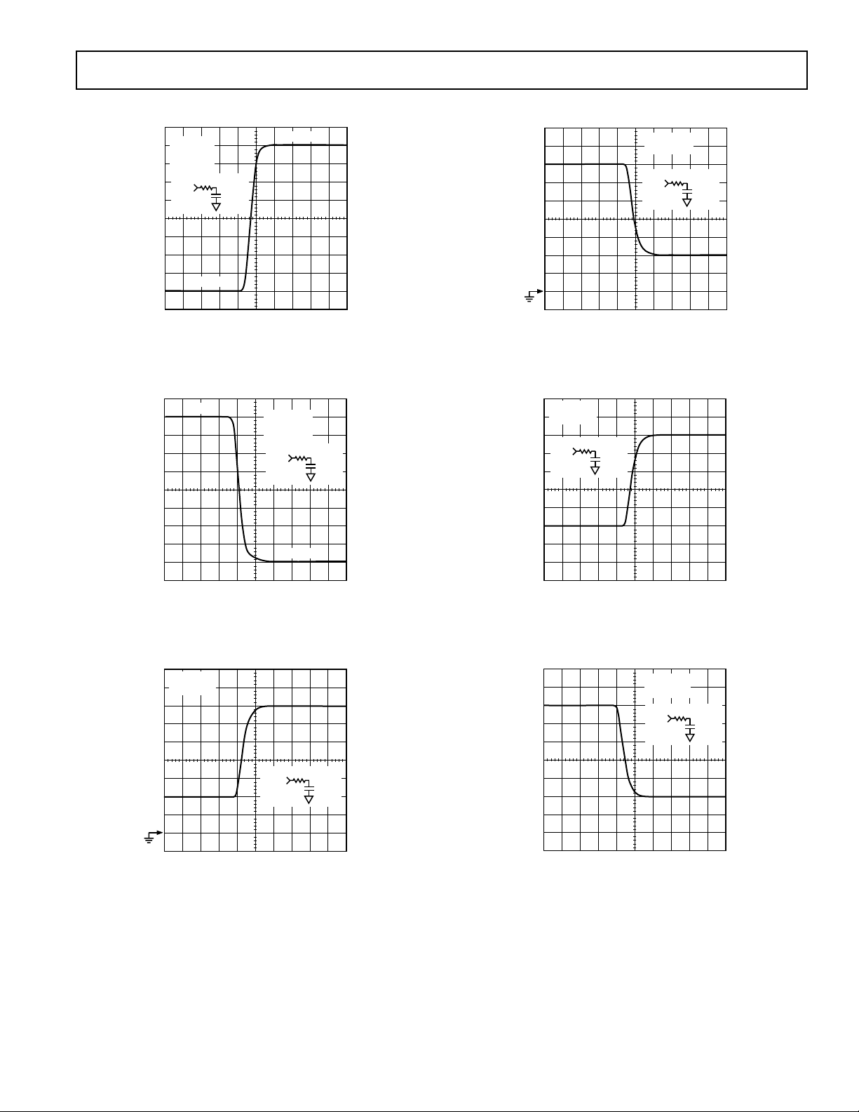
Typical Performance Characteristics–AD8380
20ns/DIV
VMID = 7V
VFS = 5V
VMID
1V/DIV
25⍀
C
L
150pF
VIDX
VMID – VFS
20ns/DIV
VMID = 7V
VFS = 5V
VMID
1V/DIV
25⍀
C
L
150pF
VIDX
VMID + VFS
20ns/DIV
VMID = 7V
VFS = 5V
VMID
1V/DIV
25⍀
C
L
150pF
VIDX
VMID + VFS
VMID + VFS
1.25V/DIV
VMID – VFS
CODE = 0
VMID = 7V
VFS = 5V
25⍀
VIDX
INV = L
C
L
150pF
20ns/DIV
INV = H
TPC 1. Invert Switching 10 V Step Response (Rise) at C
VMID + VFS
1.25V/DIV
INV = H
CODE = 0
VMID = 7V
VFS = 5V
25⍀
VIDX
C
L
150pF
TPC 4. Data Switching Full-Scale Step Response (Fall) at
L
CL, INV = L
VMID – VFS
20ns/DIV
INV = L
TPC 2. Invert Switching 10 V Step Response (Fall) at C
VMID = 7V
VFS = 5V
VMID
1V/DIV
VMID – VFS
20ns/DIV
VIDX
25⍀
C
L
150pF
TPC 3. Data Switching Full-Scale Step Response (Rise) at
CL, INV = L
TPC 5. Data Switching Full-Scale Step Response (Rise) at
L
, INV = H
C
L
TPC 6. Data Switching Full-Scale Step Response (Fall) at
CL, INV = H
REV. B
–5–
Page 6

AD8380
VMID = 7V
VFS = 5V
VFS
INV = H
t
= 0
VIDX
VMID
10ns/DIV
25⍀
VMID + VFS
C
L
150pF
VMID+
OUTPUT VOLTAGE ERROR – 1%/DIV
TPC 7. Output Settling Time Response to 1% of Full
Scale (Rising Edge) at C
VMID
OUTPUT VOLTAGE ERROR – 1%/DIV
t = 0
L
VIDX
VMID + VFS
10ns/DIV
VMID = 7V
VFS = 5V
INV = H
25⍀
C
L
150pF
VMID
TPC 8. Output Settling Time Response to 1% of Full
Scale (Falling Edge) at C
L
VMID = 7V
VFS = 5V
INV = H
25⍀
VIDX
VMID + VFS
C
L
150pF
VMID
VMID
t
OUTPUT VOLTAGE ERROR – 0.1%/DIV
= 0
10ns/DIV
TPC 10. Output Settling Time Response to 0.25% of Full
Scale (Falling Edge) at C
7.5
5.5
3.5
1.5
0
VDE – mV
–1.5
–3.5
–5.5
–7.5
06090
10 20 30 40 50 70 80
L
CODE 482
CODE 738
TEMPERATURE – ⴗC
TPC 11. Differential Error Voltage (VDE) vs. Temperature
VMID = 7V
VFS = 5V
VMID + VFS
OUTPUT VOLTAGE ERROR – 0.1%/DIV
INV = H
t = 0
VIDX
VMID
10ns/DIV
25⍀
VMID + VFS
C
L
150pF
TPC 9. Output Settling Time Response to 0.25% of Full
Scale (Rising Edge) at C
L
–6–
3.5
2.5
1.5
CODE 738
0.5
0
–0.5
VCME – mV
–1.5
–2.5
–3.5
06090
10 20 30 40 50 70 80
TEMPERATURE – ⴗC
CODE 482
TPC 12. Common-Mode Error Voltage (VCME) vs.
Temperature
REV. B
Page 7

AD8380
0.5
0.4
0.3
0.2
0.1
0
DNL – LSB
–0.1
–0.2
–0.3
–0.4
–0.5
0
CODE
896768640512384256128 1024
TPC 13. Differential Nonlinearity (DNL) vs. Code, INV = H
0.5
0.4
0.3
0.2
0.1
0
DNL – LSB
–0.1
–0.2
–0.3
–0.4
–0.5
0
CODE
896768640512384256128 1024
TPC 14. Differential Nonlinearity (DNL) vs. Code, INV = L
0.5
0.4
0.3
0.2
0.1
0
INL – LSB
–0.1
–0.2
–0.3
–0.4
–0.5
0
CODE
896768640512384256128 1024
TPC 16. Integral Nonlinearity (INL) vs. Code, INV = H
0.5
0.4
0.3
0.2
0.1
0
INL – LSB
–0.1
–0.2
–0.3
–0.4
–0.5
0
CODE
1024
896768640512384256128
TPC 17. Integral Nonlinearity (INL) vs. Code, INV = L
7.5
5.0
2.5
0
VDE – mV
–2.5
–5.0
–7.5
0
CODE
TPC 15. Differential Error Voltage (VDE) vs. Code
REV. B
3.5
2.5
0
VCME – mV
–2.5
1024
896768640512384256128
–3.5
0
CODE
1024
896768640512384256128
TPC 18. Common-Mode Error Voltage (VCME) vs. Code
–7–
Page 8

AD8380
VFS = 5V
VMID = 7V
INV = L
= 25⍀
R
1mV/DIV
2V/DIV
S
= 150pF
C
L
CLK
OUTPUT @ CODE 0
20ns/DIV
TPC 19. Clock Switching Transient (Feedthrough) at C
VFS = 5V
VMID = 7V
INV = L
= 25⍀
R
5mV/DIV
2V/DIV
S
= 150pF
C
L
OUTPUT
@ CODE 1023
DATA
VFS = 5V
VMID = 7V
INV = L
= 25⍀
R
2.5V/DIV
20mV/DIV
L
60
40
20
0
–20
PSRR – dB
–40
–60
S
= 150pF
C
L
(QUIET)
TPC 21. All-Hostile Crosstalk at C
VID0,1,2,3,4
VID5
10ns/DIV
L
VOUTP (INV = L)
VOUTN (INV = H)
20ns/DIV
TPC 20. Data Switching Transient (Feedthrough) at C
–80
10k 5M100k
L
TPC 22. AVCC Power Supply Rejection vs. Frequency
FREQUENCY – Hz
1M
–8–
REV. B
Page 9

AD8380
THEORY OF OPERATION
The AD8380 is a system building block designed to directly drive
the columns of poly-silicon LCD panels of the type popularized for use in data projectors. It comprises six channels of
precision 10-bit digital-to-analog converters loaded from a
single, high speed, 10-bit parallel input. Precision current
feedback amplifiers providing well-damped pulse responses
and rapid voltage settling into large capacitive loads buffer the
six outputs. Excellent linearity performance and laser trimming
of scale factors and output offsets at the wafer level ensure low
absolute output errors over all input codes. Tight channel-tochannel matching in high channel count systems is guaranteed
by reliance on an externally-applied voltage reference.
DB [0:9]
CLK
STSQ/CS
XFR
E/O
R/L
A[0:2]
STBY
BYP
VREFHI
VREFLO
10
CHANNEL
SELECTOR
3
BIAS
SCALING
CONTROL
AD8380
10
10
10
10
10
1010
2-STAGE
LATCH
2-STAGE
LATCH
2-STAGE
LATCH
2-STAGE
LATCH
2-STAGE
LATCH
2-STAGE
LATCH
INV VMID
DAC
10
DAC
10
DAC
10
DAC
10
DAC
10
DAC
VID0
VID1
VID2
VID3
VID4
VID5
Figure 3. Top Level Block Diagram
Transfer Function
The transfer function of the AD8380 is made up of two regions
of operation, in which the video output voltages are either above
or below an output reference voltage externally applied at the
VMID input.
(VMID + VFS)
INV = H
VOUTN
The region over which the output voltage varies with input code
is defined by the status of the INV input. When INV is low, the
video output voltages rise from (VMID – VFS), (where VFS =
the full-scale output voltage), to VMID as the input code increases
from 0 to 1023. When INV is high, the output voltages drop
from (VMID + VFS) to VMID with increasing code (see
Figure 4).
For each value of input code there are then two possible values
for the output voltage, depending on the status of INV. When
INV is low the output is defined as VOUTP(N) where N refers
to the input code, and the P refers to the positive slope of the
voltage variation with code. When INV is high, the output is
defined as VOUTN(N).
To best correlate transfer function errors to image artifacts, the
overall accuracy of the AD8380 is defined by comparing the output
voltages, VOUTP(N) and VOUTN(N), to each other and to
their ideal values. Two parameters are defined, one dependent
on the difference between the signal amplitudes at a particular
code, and one dependent on their average value. These are VDE
and VCME. Their defining expressions are:
×
VDE = [VOUTN(N) – VOUTP(N)]/2 – [(1 – N/1023)
VFS]
where
N = input code, and VFS = 2 × (VREFHI – VREFLO)
VCME = [[VOUTN(N) +VOUTP(N)]/2 – VMID] × (1/2)
where
VMID = midpoint reference voltage for the video outputs.
Setting the Full-Scale Output
The full-scale output voltage (VFS), which defines the maximum output voltage excursion for a full code input transition, is
defined as twice the voltage difference between the VREFHI and
VREFLO inputs.
Operating Modes, Control Logic and DAC Latches
Control logic included on the AD8380 chip facilitates channel
loading in ascending or descending order (for image mirroring),
data loading on rising or falling clock edges (for even/odd word
loading), and addressing and loading individual channels (for
system testing or debugging). The on-chip logic makes it easy to
build systems requiring more than six drive channels per color.
DAC latches are of a two-stage master-slave design that guarantees all channel outputs are updated simultaneously.
VMID
VOUTP
VIDEO OUTPUT VOLTAGE
(VMID – VFS)
0 1023
INPUT CODE
INV = L
Figure 4. Definition of Output Transfer Function
REV. B
–9–
Page 10

AD8380
SVGA System Operation
An SVGA system is characterized by the requirement of six
channels of panel drive for each displayed color. Such a system
would use a single AD8380 per color.
With E/O and all address bits A[0:2] set high, channel loading
commences on the first rising edge of CLK following a valid
assertion of the Start Sequence (STSQ) input. The second stage
latches, and therefore the video outputs, are updated on the
first falling edge of the clock following a valid Transfer (XFR)
signal. (See Figure 5 for signal timing details.)
DB[0:9]
CLK
STSQ/CS
XFR
5050
t1t
t
7
2.0V
0.8V
t
t
3
4
2
t
t
5
6
t
2.0V
0.8V
7
Figure 5. Sequenced SVGA Timing (A[0:2] = HIGH, E/O =
HIGH, See Table I
)
Table I. Sequenced SVGA Data Byte to Channel Assignment
Channel Number Data Byte Number
E/O = HIGH VID0 0
R/L = LOW VID1 1
VID2 2
VID3 3
VID4 4
VID5 5
Load Sequence Switching (Right/Left Control)
To facilitate image mirroring, the order in which channels are
loaded can be easily switched. When the voltage on the right/left
control input (R/L) is low, the internal sequencer will load data
starting with Channel 0 and counting up to Channel 5. When
this voltage is high, channel loading will be in reverse order, from
Channel 5 down to Channel 0.
XGA System Operation
In an XGA system, twelve column drivers (two AD8380s) are
required for each color (refer to Figure 6). An “even/odd”
system, in which one AD8380 drives even numbered columns
and another drives odd numbered columns, can be easily implemented as detailed in Figures 7 and 8. A clock at one-half the
pixel rate is applied to the CLK input. Even bytes are loaded on
the rising edge of the clock, while odd bytes are loaded on the
falling edge. Identifying whether a chip is to load on rising or falling
edges is done by setting the proper level on the E/O input.
PANEL
CONTROLLER
CLKIN
IMAGE
PROCESSOR
VIDEO
DB[0:9]
DCLK/2
10
1 COLOR OF ‘EVEN/ODD’ XGA
STSQ_A
STSQ_B
XFR
E/O_A
R/L
INV
E/O_B
STSQ/CS
XFR
E/O
R/L
INV
CLK
STSQ/CS
XFR
E/O
R/L
INV
CLK
AD8380
DEVICE “A”
DB[0:9]
AD8380
DEVICE “B”
DB[0:9]
A[0:2]
VIDEO
OUT
A[0:2]
VIDEO
OUT
DVCC
3
6
DVCC
3
6
Figure 6. Even/Odd: Outputs of Devices A and B are
Configured as Even and Odd Data Channels and Loading
O
Sequence Is Defined by Status of E /
DB[0:9]
(EVEN
STSQ
(EVEN
STSQ
CLK
CHIP)
/
CS
CHIP)
CLK
(ODD
CHIP)
/
CS
(ODD
CHIP)
XFR
A0:A2 = HIGH
10 011 9 10 11
0
t
t
4
3
t
t
4
3
and R/L Inputs
t
1
t
2
t
1
t
2
t
t
5
6
Figure 7. Sequenced Even/Odd XGA Timing, A[0:2] =
HIGH (See Table II)
Table II. Sequenced Even/Odd XGA Data Byte to
Channel Assignment
Data Byte Number
Channel Number R/L = LOW R/L = HIGH
E/O = HIGH VID0 0 10
VID1 2 8
VID2 4 6
VID3 6 4
VID4 8 2
VID5 10 0
E/O = LOW VID0 1 11
VID1 3 9
VID2 5 7
VID3 7 5
VID4 9 3
VID5 11 1
–10–
REV. B
Page 11

DCLK
AD8380
AD8380 INPUT DATA
CLK (AD8380)
/CS (EVEN)
STSQ
/CS (ODD)
STSQ
XFR
AD8380 #1
EVEN CHANNEL
(E/O = HIGH)
(R/L = LOW)
012 4 567893 1011121314 15161718192021222324
0
2
4
6
8
10
12 24
14
16
18
20
0
2
4
6
8
10
22
12
14
16
18
20
22
AD8380 #2
ODD CHANNEL
(E/O = LOW)
(R/L = LOW)
1
3
5
7
9
11
1
3
5
7
9
11
13
15
17
19
21
23
13
15
17
19
21
23
Figure 8. Operation of Even/Odd XGA System
REV. B
–11–
Page 12

AD8380
SXGA and Beyond
Very high resolution display systems can be built using the E/O
XGA system as a model. By using four AD8380s, twenty-four
columns can be driven together for an SXGA display. Two would
be designated for even columns and two for odd. Four separate
STSQ signals would be used to coordinate data loading with a
single XFR to synchronize updating of output voltages.
Using a single external voltage source to drive the VREF inputs
on all drivers for a particular color and a single voltage source
for all their VMID inputs, will guarantee matching for all channels.
The exceptional accuracy of the AD8380’s transfer function will
ensure that high channel count systems can be built without fear of
image artifacts resulting from channel-to-channel matching errors.
Direct Channel Loading
For debug or characterization purposes, it may be desirable to
load data directly into a single channel without requiring exercise
of the STSQ and XFR inputs. This can be done by applying
dc logic high levels to the STSQ and XFR inputs, and addressing
the desired channel through the A[0:2] inputs. Data will then
be loaded into the selected channel on each falling edge of the
CLK signal.
The maximum rate at which a channel can be updated will be
limited by the settling time of the output amplifiers.
Addressed Channel Loading
The direct channel loading method can be extended. Channels
may be loaded in an arbitrary sequence through the use of an
active XFR signal with STSQ set to a high level. Use the A[0:2]
inputs to define the desired channel sequence. Data will be loaded
on the falling edge of CLK into the channel whose address was
valid on the preceding rising edge of CLK. All channel outputs
are then updated together by qualification of a valid XFR signal.
See Figure 9 for timing details.
DB[0:9]
CLK
XFR
A[0:2]
IN THIS CASE, INPUT LATCHES ARE LOADED IN THE ORDER SELECTED
BY A[0:2], THEN DACs ARE UPDATED TOGETHER BY XFR.
50 1 5
t
t
1
2
t
5
t
6
t8t
9
0
Figure 9. Addressed Channel Timing (E/O = HIGH,
STSQ/CS = HIGH)
Standby Mode
A high level applied to the standby (STBY) input will turn off
most of the internal circuitry, dropping the quiescent power
dissipation to a few milliwatts. Since both digital and analog
circuits are debiased, all stored data will be lost. Upon returning
STBY to a low level, normal operation is restored.
APPLICATION
The AD8380 is a mixed-signal, high speed, very accurate device
with multiple channels. In order to realize its specifications, it is
essential to use a properly designed circuit board.
Layout and Grounding
The analog and digital sections of the AD8380 are pinned
out on approximately opposite sides of the package. When
laying out a circuit board, please keep these sections separate
from each other to minimize crosstalk and noise coupling of
the digital input signals into the analog outputs.
All signal trace lengths should be made as short and direct as
possible to prevent signal degradation due to parasitic effects.
Please note that digital signals should not cross or be routed
near analog signals.
It is imperative to provide a solid ground plane under and
around the part. All of the ground pins of the part should be
directly connected to the ground plane with no extra signal
path length. For conventional operation, this includes the
pins DVEE, AVEEDAC, AVEEBIAS, AVEE0, AVEE1,2;
AVEE3,4; and AVEE5. The return currents for any of the signals for the part should be routed close to the ground pin for
that section to prevent stray signals from appearing on other
ground pins.
Power Supply Bypassing
The AD8380 has several power supply and reference voltages
that must be properly bypassed to the ground plane for optimum performance. The bypass capacitor for each supply pin, as
well as VREFHI, VREFLO, and VMID, should be connected as
close as possible to the IC pins and directly to the ground plane.
A 0.1 µF capacitor, preferably a ceramic chip, should be used to
minimize lead length.
To provide low frequency, high current bypassing, larger value
tantalum capacitors should also be used. These should be connected from the supply to ground, but it is not necessary to place
these close to the IC pins. Stray inductance will not greatly affect
their performance. The high current outputs should be bypassed
with these capacitors. It is recommended that two 22 µF tantalum
capacitors be placed from the AVCC supply to ground at either
end of the output side of the IC. AVCCBIAS and AVCCDAC
should each have a 10 µF tantalum bypass capacitor to ground.
See Figure 10.
VREFHI Reference Distribution
In a system that uses more than one AD8380 per color, it is
important that all of the AD8380 devices operate from equal
reference voltages to ensure that the video outputs are well
matched. VREFLO is not a concern due to its high input resistance and very low bias current. Therefore, it is not likely that
there will be significant dc voltage drops in the circuit traces to that
supply. It is recommended to have good local supply bypassing
at each AD8380 from their respective VREFLOs to ground.
The higher input current that flows in the VREFHI circuit
requires that this be laid out more carefully. VREFHI connects
internally to a 20 kΩ resistor for each of the six channels to provide
an input resistance of about 3.3 kΩ. Thus with a (VREFHI –
VREFLO) voltage of 2.5 V (to yield a VFS of 5.0 V ), about
750 µA will flow into each VREFHI circuit.
–12–
REV. B
Page 13

AD8380
2.500V
3.3V
10V
15V
CLK
10
DB[0:9]
XFR
E/O
R/L
STSQ/CS
3
A[0:2]
INV
STBY
0.1F
DVCC
VREFHI VREFLO AVCCDAC AVCCBIAS AVCC0,1 AVCC2,3 AVCC4,5 VMID
DVEE AVEEDAC BYP AVEEBIAS AVEE0
AVEE1,2 AVEE3,4
AVEE5
LOGIC
DAC
BIAS DRIVERS
6
VID0 – VID5
7V
10F
0.1F 0.1F 0.1F 0.1F
0.1F
22F
10F0.1F
R
S
24.9⍀
(TYP FOR 6)
10F 22F10F
0.1F0.1F0.1F
In order to obtain the best matching, the traces to each of the
VREFHI pins of the AD8380s should be connected by an
approximately same length and same width circuit trace in a
“star” configuration. The source of the VREFHI voltage should
be at the center of the “star.” Therefore, the VREFHI currents
for two devices will not share a significant length of circuit trace,
and each trace will provide an approximately equal voltage drop.
In addition, if the VREFHI traces must be long, then the traces
should be widened to minimize differences in the voltage drops
due to differences in the VREFHI input currents of different
AD8380s. The dc resistance of these traces should be less than
100 mΩ. If the VREFHI input current is about 1 mA, then the
voltage drop will be about 100 µV.
For example, if a trace length is 5 in. long (13 cm.), then the
trace width for a 1 oz. copper foil should be wider than 0.025 in.
(0.7 mm) in order to keep the trace impedance below 100 mΩ.
Driving a Capacitive Load
A purely capacitive load can react with output impedance of the
AD8380 resulting in overshoot and ringing in its step response.
To minimize this effect, and optimize settling time, it is recommended that a 25 Ω resistor be placed in series with each of the
driver’s outputs as shown in Figure 10.
Figure 10. Interface Drawing
REV. B
–13–
Page 14

AD8380
OUTLINE DIMENSIONS
Dimensions shown in inches and (mm).
44-Lead MQFP
(S-44A)
0.041 (1.03)
0.029 (0.73)
SEATING
PLANE
0.010 (0.25)
MAX
0.009 (0.23)
0.005 (0.13)
0.096 (2.45)
MAX
0.083 (2.10)
0.077 (1.95)
1
11
12
0.031 (0.80)
0.530 (13.45)
0.510 (12.95)
0.398 (10.10)
0.390 (9.90)
TOP VIEW
(PINS DOWN)
BSC
SQ
SQ
0.018 (0.45)
0.012 (0.30)
3444
33
0.315 (8.00)
REF
23
22
AD8380–Revision History
Location Page
Data sheet changed from REV. A to REV B.
Single-Channel Block Diagram section and graphic removed . . . . . . . . . . . . . . . . . . . . . . . . . . . . . . . . . . . . . . . . . . . . . . . . . . . . . . 9
–14–
REV. B
Page 15

–15–
Page 16

C01091–0–4/01(B)
–16–
PRINTED IN U.S.A.
 Loading...