

Page 1
A0A1A2A3A
VCCA
–
www.BDTIC.com/ADI
Ultralow Distortion IF Dual VGA
FEATURES
Dual independent digitally controlled VGAs
Bandwidth of 700 MHz (−3 dB)
Gain range: −4 dB to +20 dB
Step size: 1 dB ± 0.2 dB
Differential input and output
Noise figure: 8.7 dB @ maximum gain
Output IP3 of ~50 dBm at 200 MHz
Output P1dB of 20 dBm at 200 MHz
Dual parallel 5-bit control interface
Provides constant SFDR vs. gain
Power-down control
Single 5 V supply operation
32-lead, 5 mm x 5 mm LFCSP
APPLICATIONS
Differential ADC drivers
Main and diversity IF sampling receivers
Wideband multichannel receivers
Instrumentation
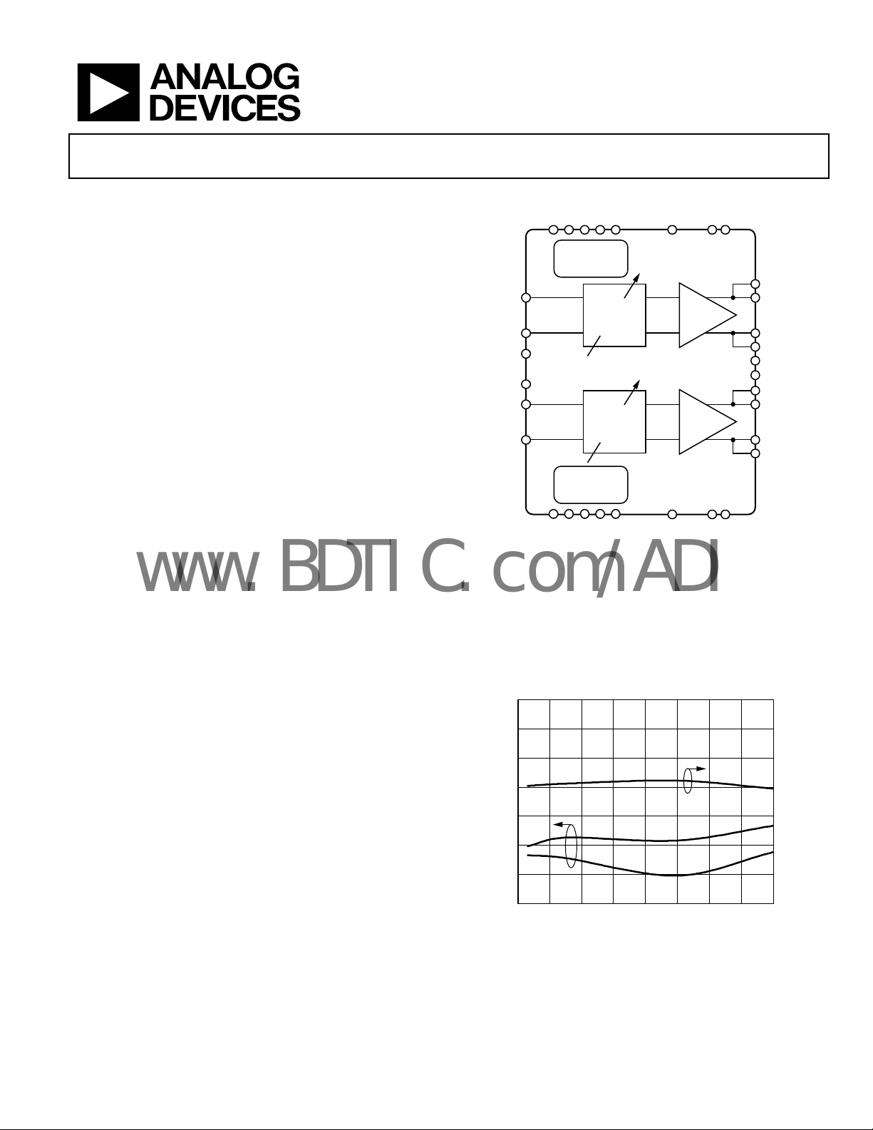
GENERAL DESCRIPTION
The AD8376 is a dual channel, digitally controlled, variable gain
wide bandwidth amplifier that provides precise gain control,
high IP3, and low noise figure. The excellent distortion performance and high signal bandwidth make the AD8376 an excellent
gain control device for a variety of receiver applications.
Using an advanced high speed SiGe process and incorporating
roprietary distortion cancellation techniques, the AD8376
p
achieves 50 dBm output IP3 at 200 MHz.
The AD8376 provides a broad 24 dB gain range with 1 dB
solution. The gain of each channel is adjusted through
re
dedicated 5-pin control interfaces and can be driven using
standard TTL levels. The open-collector outputs provide a
flexible interface, allowing the overall signal gain to be set by
the loading impedance. Thus, the signal voltage gain is directly
proportional to the load.
Each channel of the AD8376 can be individually powered on by
pplying the appropriate logic level to the ENBA and ENBB
a
power enable pins. The quiescent current of the AD8376 is
typically 130 mA per channel. When powered down, the
AD8376
FUNCTIONAL BLOCK DIAGRAM
4
CHANNEL A
GAIN
DECODER
IPA+
α
IPA–
VCMA
VCMB
IPB+
α
IPB–
CHANNEL B
GAIN
DECODER
B0B1B2B3B4
Figure 1.
AD8376 consumes less than 5 mA and offers excellent input-tooutput isolation, lower than −50 dB at 200 MHz.
Fabricated on an Analog Devices, Inc., high speed SiGe process,
th
e AD8376 is supplied in a compact, thermally enhanced,
5 mm × 5mm 32-lead LFCSP package and operates over the
temperature range of −40°C to +85°C.
40
–50
–60
–70
–80
–90
–100
HARMONIC DISTO RTION (dBc), OUTPUT @ 2V p-p
–110
40 60 80 100 120 140 160 180 200
Figure 2. Harmonic Distortion and Output IP3 vs. Frequency
FREQUENCY (MHz )
OIP3
HD2
HD3
AD8376
POST-AMP
POST-AMP
GNDA
GNDBVCCB
OPA+
OPA+
OPA–
OPA–
ENBA
ENBB
OPB+
OPB+
OPB–
OPB–
06725-001
65
60
55
50
45
40
OIP3 (dBm), OUTPUT @ 3dBm/TONE
35
30
06725-052
Rev. 0
Information furnished by Analog Devices is believed to be accurate and reliable. However, no
responsibility is assumed by Anal og Devices for its use, nor for any infringements of patents or ot her
rights of third parties that may result from its use. Specifications subject to change without notice. No
license is granted by implication or otherwise under any patent or patent rights of Analog Devices.
Trademarks and registered trademarks are the property of their respective owners.
One Technology Way, P.O. Box 9106, Norwood, MA 02062-9106, U.S.A.
Tel: 781.329.4700 www.analog.com
Fax: 781.461.3113 ©2007 Analog Devices, Inc. All rights reserved.
Page 2

AD8376
www.BDTIC.com/ADI
TABLE OF CONTENTS
Features .............................................................................................. 1
Applications....................................................................................... 1
Functional Block Diagram .............................................................. 1
General Description......................................................................... 1
Revision History ............................................................................... 2
Specifications..................................................................................... 3
Absolute Maximum Ratings............................................................ 5
ESD Caution.................................................................................. 5
Pin Configuration and Function Descriptions............................. 6
Typical Performance Characteristics............................................. 7
Circuit Description......................................................................... 12
REVISION HISTORY
8/07—Revision 0: Initial Version
Basic Structure............................................................................ 12
Applications..................................................................................... 13
Basic Connections...................................................................... 13
Single-Ended-to-Differential Conversion............................... 13
Broadband Operation................................................................ 15
ADC Interfacing......................................................................... 15
Layout Considerations............................................................... 18
Characterization Test Circuits.................................................. 18
Evaluation Board ........................................................................ 19
Outline Dimensions .......................................................................23
Ordering Guide .......................................................................... 23
Rev. 0 | Page 2 of 24
Page 3
AD8376
www.BDTIC.com/ADI
SPECIFICATIONS
VS = 5 V, T = 25°C, RS = RL = 150 Ω at 140 MHz, 2 V p-p differential output, both channels enabled, unless otherwise noted.
Table 1.
Parameter Conditions Min Typ Max Unit
DYNAMIC PERFORMANCE
−3 dB Bandwidth V
Slew Rate 5 V/ns
INPUT STAGE Pin IPA+ and Pin IPA−, Pin IPB+ and Pin IPB−
Maximum Input Swing For linear operation (AV = −4 dB) 8.5 V p-p
Differential Input Resistance Differential 120 150 165 Ω
Common-Mode Input Voltage 1.85 V
CMRR Gain code = 00000 45.5 dB
GAIN
Amplifier Transconductance Gain code = 00000 0.060 0.067 0.074 S
Maximum Voltage Gain Gain code = 00000 20 dB
Minimum Voltage Gain Gain code ≥ 11000 −4 dB
Gain Step Size From gain code = 00000 to 11000 0.93 0.98 1.02 dB
Gain Flatness All gain codes, 20% fractional bandwidth for fC < 200 MHz 0.18 dB
Gain Temperature Sensitivity Gain code = 00000 8 mdB/°C
Gain Step Response For VIN = 100 mV p-p, gain code = 10100 to 00000 5 ns
OUTPUT STAGE Pin OPA+ and Pin OPA−, Pin OPB+ and Pin OPB−
Output Voltage Swing At P1dB, gain code = 00000 13.1 V p-p
Output Impedance Differential 16||0.8 kΩ||pF
Channel Isolation
NOISE/HARMONIC PERFORMANCE
46 MHz Gain code = 00000
Noise Figure 8.7 dB
Second Harmonic V
Third Harmonic V
Output IP3 2 MHz spacing, 3 dBm per tone 50 dBm
Output 1 dB Compression Point 21.3 dBm
70 MHz Gain code = 00000
Noise Figure 8.7 dB
Second Harmonic V
Third Harmonic V
Output IP3 2 MHz spacing, 3 dBm per tone 50 dBm
Output 1 dB Compression Point 21.4 dBm
140 MHz Gain code = 00000
Noise Figure 8.7 dB
Second Harmonic V
Third Harmonic V
Output IP3 2 MHz spacing, 3 dBm per tone 51 dBm
Output 1 dB Compression Point
200 MHz Gain code = 00000
Noise Figure 8.7 dB
Second Harmonic V
Third Harmonic V
Output IP3 2 MHz spacing, 3 dBm per tone 50 dBm
Output 1 dB Compression Point 20.9 dBm
< 2 V p-p (5.2 dBm) 700 MHz
OUT
Measured at differential output f
applied to alternate channel (referred to output)
= 2 V p-p −92 dBc
OUT
= 2 V p-p −94 dBc
OUT
= 2 V p-p −89 dBc
OUT
= 2 V p-p −95 dBc
OUT
= 2 V p-p −87 dBc
OUT
= 2 V p-p −97 dBc
OUT
= 2 V p-p −82 dBc
OUT
= 2 V p-p −91 dBc
OUT
or differential input
73 dB
21.6
dBm
Rev. 0 | Page 3 of 24
Page 4

AD8376
www.BDTIC.com/ADI
Parameter Conditions Min Typ Max Unit
POWER INTERFACE
Supply Voltage
VCC and Output Quiescent Current
with Both Channels Enabled
vs. Temperature −40°C ≤ TA ≤ +85°C
Power-Down Current, Both Channels ENBA and ENBB Low
vs. Temperature −40°C ≤ TA ≤ +85°C
POWER-UP/GAIN CONTROL Pin A0 to Pin A4, Pin B0 to Pin B4, Pin ENBA, and Pin ENBB
V
IH
V
IL
Logic Input Bias Current 900 nA
Table 2. Gain Code vs. Voltage Gain Look-Up Table
5-Bit Binary Gain Code Voltage Gain (dB)
00000 +20
00001 +19
00010 +18
00011 +17
00100 +16
00101 +15
00110 +14
00111 +13
01000 +12
01001 +11
01010 +10
01011 +9
01100 +8
Thermal connection made to exposed paddle under device 245 250 255 mA
Minimum voltage for a logic high 1.6
Maximum voltage for a logic low
5-Bit Binary Gain Code Voltage Gain (dB)
01101 +7
01110 +6
01111 +5
10000 +4
10001 +3
10010 +2
10011 +1
10100 0
10101 −1
10110 −2
10111 −3
11000 −4
>11000 −4
4.5 5.0 5.5 V
5.4
285 mA
7 mA
0.8 V
mA
V
Rev. 0 | Page 4 of 24
Page 5
AD8376
www.BDTIC.com/ADI
ABSOLUTE MAXIMUM RATINGS
Table 3.
Parameter Rating
Supply Voltage, V
ENBA, ENBB, A0 to A4, B0 to B4 −0.6 V to (V
Input Voltage, V
DC Common Mode VCMA, VCMB ± 0.25 V
VCMA, VCMB ± 6 mA
Internal Power Dissipation 1.6 W
θJA (Exposed Paddle Soldered Down) 34.6°C/W
θJC (At Exposed Paddle) 3.6°C/W
Maximum Junction Temperature 140°C
Operating Temperature Range −40°C to +85°C
Storage Temperature Range −65°C to +150°C
IN+
POS
, V
IN−
5.5 V
+ −0.6 V)
POS
−0.15 V to +4.15 V
Stresses above those listed under Absolute Maximum Ratings
may cause permanent damage to the device. This is a stress
rating only; functional operation of the device at these or any
other conditions above those indicated in the operational
section of this specification is not implied. Exposure to absolute
maximum rating conditions for extended periods may affect
device reliability.
ESD CAUTION
Rev. 0 | Page 5 of 24
Page 6
AD8376
V
www.BDTIC.com/ADI
PIN CONFIGURATION AND FUNCTION DESCRIPTIONS
A
GNDA
IPA+
IPA–
A0
29
31
30
PIN 1
INDICATOR
AD8376
TOP VIEW
11
10
12
B0
IPB–
IPB+
VCC
OPA+
OPA–
28
27
26
25
24 OPA+
23 OPA–
22 ENBA
21 GNDA
20 GNDB
19 ENBB
18 OPB–
17 OPB+
13
14
15
16
OPB–
OPB+
VCCB
GNDB
A1
32
1A2
2A3
3A4
4VCMA
5
CMB
6B4
(Not to Scal e)
7B3
8B2
9
B1
Figure 3. 32-Lead LFCSP
Table 4. Pin Function Descriptions
Pin No. Mnemonic Description
1 A2 MSB − 2 for the Gain Control Interface for Channel A.
2 A3 MSB − 1 for the Gain Control Interface for Channel A.
3 A4
4 VCMA
5 VCMB
6 B4
7 B3
8 B2
9 B1
10 B0
11 IPB+
12 IPB−
13, 20 GNDB
14 VCCB
15, 17 OPB+
16, 18 OPB−
19 ENBB
21, 28 GNDA
22 ENBA
23, 25 OPA−
24, 26 OPA+
27 VCCA
29 IPA−
30 IPA+
31 A0
MSB for the 5-Bit Gain Control Interface for Channel A.
Channel A Input Common-Mode Voltage. Typically bypassed to ground through capacitor.
Channel B Input Common-Mode Voltage. Typically bypassed to ground through capacitor.
MSB for the 5-Bit Gain Control Interface for Channel B.
MSB − 1 for the Gain Control Interface for Channel B.
MSB − 2 for the Gain Control Interface for Channel B.
LSB + 1 for the Gain Control Interface for Channel B.
LSB for the Gain Control Interface for Channel B.
Channel B Positive Input.
Channel B Negative Input.
Device Common (DC Ground) for Channel B.
Positive Supply Pin for Channel B. Should be bypassed to ground using suitable bypass capacitor.
Positive Output Pins (Open Collector) for Channel B. Require dc bias of +5 V nominal.
Negative Output Pins (Open Collector) for Channel B. Require dc bias of +5 V nominal.
Power Enable Pin for Channel B. Channel B is enabled with a logic high and disabled with a logic low.
Device Common (DC Ground) for Channel A.
Power Enable Pin for Channel A. Channel A is enabled with a logic high and disabled with a logic low.
Negative Output Pins (Open Collector) for Channel A. Require dc bias of +5 V nominal.
Positive Output Pins (Open Collector) for Channel A. Require dc bias of +5 V nominal.
Positive Supply Pins for Channel A. Should be bypassed to ground using suitable bypass capacitor.
Channel A Negative Input.
Channel A Positive Input.
LSB for the Gain Control Interface for Channel A.
32 A1 LSB + 1 for the Gain Control Interface for Channel A.
6725-002
Rev. 0 | Page 6 of 24
Page 7
AD8376
www.BDTIC.com/ADI
TYPICAL PERFORMANCE CHARACTERISTICS
VS = 5 V, TA = 25°C, RS = RL = 150 Ω, 2 V p-p output, maximum gain unless otherwise noted.
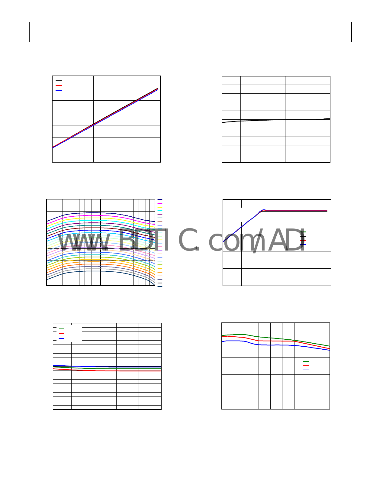
25
46MHz, +5V
70MHz, +5V
20
140MHz, +5V
15
10
5
GAIN (dB)
0
–5
–10
–4
11000010100
5
01111
GAIN CODE
10
01010
15
00101
Figure 4. Gain vs. Gain Code at 46 MHz, 70 MHz, and 140 MHz
20
00000
06725-003
1.0
0.8
0.6
0.4
0.2
0
–0.2
GAIN ERROR (dB)
–0.4
–0.6
–0.8
–1.0
–4
11000010100
5
01111
GAIN CODE
10
01010
15
00101
Figure 7. Gain Step Error, Frequency 140 MHz
20
00000
06725-006
25
20
15
10
5
GAIN (dB)
0
–5
–10
10 100 1000
10
9
25°C
8
85°C
7
–40°C
6
5
4
3
2
1
0
–1
–2
–3
GAIN ERROR (dB)
–4
–5
–6
–7
–8
–9
–10
–4
11000010100
FREQUENCY (MHz)
Figure 5. Gain vs. Frequency Respo
5
01111
GAIN CODE
10
01010
nse
15
00101
Figure 6. Gain Error over Temperature at 140 MHz
20
00000
20dB
19dB
18dB
17dB
16dB
15dB
14dB
13dB
12dB
11dB
10dB
9dB
8dB
7dB
6dB
5dB
4dB
3dB
2dB
1dB
0dB
–1dB
–2dB
–3dB
–4dB
25
INPUT MAX
RATING
20
BOUNDARY
15
10
OP1dB (dBm)
5
0
06725-004
–4 1 6 11 16 21
GAIN (dB)
200MHz
140MHz
70MHz
46MHz
06725-007
Figure 8. P1dB vs. Gain at 46 MHz, 70 MHz, 140 MHz, and 200 MHz
25
20
15
10
OP1dB (dBm)
5
0
46 100 150 200 250 3 00 350 400 450 500
06725-005
FREQUENCY (MHz)
+25°C
+85°C
–40°C
06725-008
Figure 9. P1dB vs. Frequency at Maximum Gain, Three Temperatures
Rev. 0 | Page 7 of 24
Page 8
AD8376
–
–
www.BDTIC.com/ADI
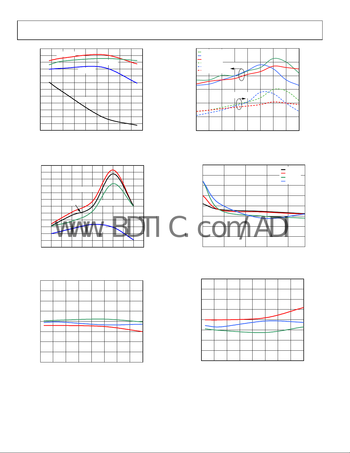
52
51
50
49
48
47
46
45
OIP3 (dBm)
44
43
42
41
40
30 50 70 90 110 130 150 170 190 21 0
AV = +20dB
AV = +10dB
AV = 0dB
AV = –4dB
FREQUENCY (MHz)
Figure 10. Output Third-Order Intercept at Four Gains,
Output Level
52
51
50
49
48
47
46
45
OIP3 (dBm)
44
43
42
41
40
–4 –3 –2 –1 0 1 2 3 4 5 6
AV = +10dB
at 3 dBm/Tone
AV = +20dB
AV = –4dB
(dBm)
P
OUT
AV = 0dB
Figure 11. Output Third-Order Intercept vs. Power
at Fou
r Gains, Frequency 140 MHz
55
+25°C 20d B
–40°C 20d B
+85°C 20d B
50
+25°C 0dB
–40°C 0d B
+85°C 0dB
45
40
OIP3 (dBm)
35
30
25
–3 –2 –1 0 1 2 3 4 5
06725-009
AV = 20dB
AV = 0dB
P
PER TONE (dBm)
OUT
Figure 13. Output Third-Order Intercept vs. Power,
Freque
ncy 140 MHz, Three Temperatures
70
–75
–80
–85
–90
IMD3 (dBc)
–95
–100
–105
–110
–4 1 6 11 16
06725-010
at 4
6 MHz, 70 MHz, 140 MHz, and 200 MHz, Output Level at 3 dBm/Tone
Figure 14. Two-Tone Output IMD vs. Gain
GAIN (dB)
46MHz
70MHz
140MHz
200MHz
65
60
55
50
OIP3 (dBm)
45
40
35
06725-012
06725-013
70
65
60
55
50
OIP3 (dBm)
45
40
35
30
40 60 80 100 120 140 160 180 200
FREQUENCY (MHz)
+25°C
+85°C
Figure 12. Output Third-Order Intercept vs. Frequency,
e Temperatures, Output Level at 3 dBm/Tone
Thre
–40°C
06725-011
Rev. 0 | Page 8 of 24
70
–75
–80
–85
–90
IMD3 (dBc)
–95
–100
–105
–110
40 60 80 100 120 140 160 180 200
FREQUENCY (MHz)
+85°C
–40°C
+25°C
Figure 15. Two-Tone Output IMD vs. Frequency,
Thre
e Temperatures, Output Level at 3 dBm/Tone
06725-014
Page 9

AD8376
–
–
–
–
–
–
–
www.BDTIC.com/ADI
–80
–85
–90
75
HD2 –4dB
HD2 0dB
HD2 +10dB
HD2 +20dB
–70
–75
–80
65
–85
–90
–95
80
HD2 –40 °C
HD2 +85°C
HD2 +25 °C
70
–75
–80
–85
–95
HD3 –4dB
–100
–105
HARMONIC DISTO RTION HD2 (d Bc)
–110
–115
40 60 80 100 120 140 160 180 200
FREQUENCY (MHz)
HD3 0dB
HD3 +10dB
HD3 +20dB
Figure 16. Harmonic Distortion vs. Frequency at Four Gain Codes,
= 2 V p-p
V
OUT
80
HD2_+20dB
HD2_+10dB
–85
HD2_0dB
HD2_–M4dB
–90
–95
–100
HARMONIC DIST ORTIO N HD2 (dBc)
–105
–110
–115
–120
–125
–130
HD3_+20dB
HD3_+10dB
HD3_0dB
HD3_–4dB
–5 –4 –3 –2 –1 0 1 2 3 4 5
P
(dBm)
OUT
Figure 17. Harmonic Distortion vs. Power at Four Gain Codes,
Freque
ncy 140 MHz
–85
–90
–95
–100
–105
60
–65
–70
–75
–80
–85
–90
–95
–100
–105
–110
HARMONIC DISTO RTION HD3 (d Bc)
HARMONIC DIST ORTIO N HD3 (dBc)
–100
–105
–110
HARMONIC DISTORTION HD2 (d Bc)
–115
–120
6725-015
–5–4–3–2–1012345
HD3 –40 °C
HD3 +25°C
HD3 +85° C
P
OUT
(dBm)
–90
–95
–100
–105
–110
HARMONIC DISTO RTION HD3 (d Bc)
06725-018
Figure 19. Harmonic Distortion vs. Power, Frequency 140 MHz,
Thre
e Temperatures
40
35
30
25
20
15
NOISE FIGURE (dB)
10
5
0
–4–2 0 2 4 6 8 101214161820
6725-016
46MHz
70MHz
140MHz
200MHz
GAIN (dB)
6725-019
Figure 20. NF vs. Gain at 46 MHz, 70 MHz, 140 MHz, and 200 MHz
70
–75
–80
–85
–90
–95
–100
–105
HARMONIC DISTO RTION HD2 AND HD3 (dBc)
–110
40 60 80 100 120 140 160 180 200
FREQUENCY (MHz)
HD2 +25°C
HD3 +25°C
HD2 –40°C
HD3 –40°C
HD2 +85°C
HD3 +85°C
Figure 18. Harmonic Distortion vs. Frequency, Three Temperatures,
= 2 V p-p
V
OUT
6725-017
Rev. 0 | Page 9 of 24
45
40
35
30
25
20
15
NOISE FI GURE (dB)
10
5
0
0 100 200 300 400 500 600 700 800 900 1000
AV = –4dB
AV = 0dB
AV = +10dB
AV = +20dB
FREQUENCY (MHz)
Figure 21. NF vs. Frequency
06725-020
Page 10

AD8376
www.BDTIC.com/ADI
REF3 POSITION
–600mV/DIV
REF3 SCALE
0pF
10pF EACH SIDE
500mV
2
1
CH1 500mV Ω CH2 500mV Ω M10.0ns 10.0G S/s IT 10.0ps/ pt
A CH1 960mV
Figure 22. Gain Step Time Domain Response
2
1
CH1 500mV Ω CH2 500mV Ω M20.0n s 10.0GS/ s IT 20. 0ps/pt
A CH1 960mV
Figure 23. ENBL Time Domain Response
INPUT
R1
R3
06725-021
REF3 500mV 2.5n s
M2.5ns 20.0GS/s IT 10.0ps/pt
A CH4 28.0mV
06725-024
Figure 25. Pulse Response to Capacitive Loading, Gain 20 dB
REF1 PO SITI ON
–1.08/DIV
REF1 SCALE
OUTPUT
2
REF1
CH2 500mV M2.5n s 20Gsps
06725-022
REF1 50.0mV
INPUT
IT 2.5ps/ pt
50mV
RISE (C2) 1. 339ns
FALL(C2) 1.367n s
A CH2 –590mV
06725-025
Figure 26. Large Signal Pulse Response
REF1 POSITIO N
–420mV/DIV
REF1 SCALE
2V
R1
R3
R4
REF 1 2.0V 2.5ns
INPUT
0pF
10pF EACH SIDE
M2.5ns 20.0GS/s IT 10.0ps/ pt
A CH4 28.0mV
Figure 24. Pulse Response to Capacitive Loading, Gain −4 dB
06725-023
Rev. 0 | Page 10 of 24
0
–5
–10
–15
S11 MAG (dB)
–20
–25
–30
10 100 1000
FREQUENCY (MHz )
Figure 27. S11 vs. Frequency
180
120
60
0
–60
–120
–180
S11 PHASE (Degrees)
06725-026
Page 11

AD8376
–
www.BDTIC.com/ADI
0
10
–20
–40
–60
S12 (dB)
–80
–100
–120
0 100 200 300 400 500 600 700 800 900 1000
FREQUENCY (MHz)
Figure 28. Reverse Isolation vs. Frequency
0
–10
–20
–30
–40
–50
–60
ISOLATI ON (dB)
–70
–80
–90
–100
10 100 1000
FREQUENCY (MHz)
Figure 29. Off-State Isolation vs. Frequency
–20
–30
–40
–50
–60
ISOLATI ON (dB)
–70
–80
–90
0 200 400 600 800 900100 300 500 700 1000
06725-027
AV = –4dB
AV = 0dB
AV = +10dB
AV = +20dB
FREQUENCY (MHz)
06725-032
Figure 31. Channel Isolation (Output to Output) vs. Frequency
60
50
40
30
CMRR (dB)
20
10
0
0 200 400 600 800 900100 300 500 700 1000
06725-028
Figure 32. Common-Mode Rejectio
FREQUENCY (MHz)
n Ratio vs. Frequency
06725-031
1.00E–09
9.00E–10
8.00E–10
7.00E–10
6.00E–10
5.00E–10
4.00E–10
DELAY (Seco nds)
3.00E–10
2.00E–10
1.00E–10
0.00E+00
0dB, 5V, 25° C
+10dB, 5V, 25°C
+20dB, 5V, 25°C
–4dB, 5V, 25°C
0 100 200 300 400 500 600 700 800 900 1000
FREQUE NCY (MHz )
Figure 30. Group Delay vs. Frequency at Gain
6725-029
Rev. 0 | Page 11 of 24
Page 12

AD8376
VCM
www.BDTIC.com/ADI
CIRCUIT DESCRIPTION
BASIC STRUCTURE
The AD8376 is a dual differential variable gain amplifier with
each amplifier consisting of a 150 digitally controlled passive
attenuator followed by a highly linear transconductance
amplifier.
ATTENUATOR
IP+
IP–
Input System
The dc voltage level at the inputs of the AD8376 is set by an
internal voltage reference circuit to about 2 V. This reference is
accessible at VCMA and VCMB and can be used to source or
sink 100 A. For cases where a common-mode signal is applied
to the inputs, such as in a single-ended application, an external
capacitor between VCMA/VCMB and ground is required. The
capacitor improves the linearity performance of the part in this
mode. This capacitor should be sized to provide a reactance of
10 or less at the lowest frequency of operation. If the applied
common-mode signal is dc, its amplitude should be limited to
0.25 V from VCMA/VCMB (VCMA or VCMB ± 0.25 V). Each
device can be powered down by pulling the ENBA or ENBB pin
down to below 0.8 V. In the powered down mode, the total
current reduces to 3 mA (typical). The dc level at the inputs and
at VCMA/VCMB remains at about 2 V, regardless of the state of
the ENBA of ENBB pin.
Output Amplifier
The gain is based on a 150 differential load and varies as RL is
changed per the following equations:
Voltage Gain =
and
Power Gain = 10 × (log(R
1/2 AD8376
MUX BUFFERS
A0 TO A4
DIGITAL
SELECT
Figure 33. Simplifi
20 × (log(R
/150) + 2)
L
ed Schematic
/150) + 1)
L
gm CORE
AMP
OP+
OP–
06725-033
The dependency of the gain on the load is due to the open-
llector architecture of the output stage.
co
The dc current to the outputs of each amplifier is supplied
t
hrough two external chokes. The inductance of the chokes and
the resistance of the load determine the low frequency pole of
the amplifier. The parasitic capacitance of the chokes adds to
the output capacitance of the part. This total capacitance in
parallel with the load resistance sets the high frequency pole of
the device. Generally, the larger the inductance of the choke, the
higher its parasitic capacitance. Therefore, the value and type of
the choke should be chosen keeping this trade-off in mind.
For operation frequency of 15 MHz to 700 MHz driving a
150 lo
ad, 1 H chokes with SRF of 160 MHz or higher are
recommended (such as 0805LS-102XJBB from Coilcraft).
The supply current of each amplifier consists of about 50 mA
th
rough the VCC pin and 80 mA through the two chokes
combined. The latter increases with temperature at about
2.5 mA per 10°C.
Each amplifier has two output pins for each polarity, and they
a
re oriented in an alternating fashion. When designing the
board, care should be taken to minimize the parasitic capacitance due to the routing that connects the corresponding
outputs together. A good practice is to avoid any ground or
power plane under this routing region and under the chokes to
minimize the parasitic capacitance.
Gain Control
Two independent 5-bit binary codes change each attenuator
setting in 1 dB steps such that the gain of each amplifier
changes from +20 dB (Code 0) to −4 dB (Code 24 and higher).
The noise figure of each amplifier is about 8 dB at maximum
in setting, and it increases as the gain is reduced. The increase
ga
in noise figure is equal to the reduction in gain. The linearity of
the part measured at the output is first-order independent of
the gain setting. From 0 dB to 20 dB gain, OIP3 is approximately
50 dBm into 150 load at 140 MHz (3 dBm per tone). At gain
settings below 0 dB, it drops to approximately 45 dBm.
Rev. 0 | Page 12 of 24
Page 13

AD8376
V
–
www.BDTIC.com/ADI
APPLICATIONS
BASIC CONNECTIONS
Figure 36 shows the basic connections for operating the
AD8376. A voltage between 4.5 V and 5.5 V should be applied
to the supply pins. Each supply pin should be decoupled with at
least one low inductance, surface-mount ceramic capacitor of
0.1 F placed as close as possible to the device.
The outputs of the AD8376 are open collectors that need to be
ulled up to the positive supply with 1 µH RF chokes. The differ-
p
ential outputs are biased to the positive supply and require accoupling capacitors, preferably 0.1 µF. Similarly, the input pins
are at bias voltages of about 2 V above ground and should be accoupled as well. The ac-coupling capacitors and the RF chokes are
the principle limitations for operation at low frequencies.
To enable each channel of the AD8376, the ENBA or ENBB pin
ust be pulled high. Taking ENBA or ENBB low puts the
m
channels of the AD8376 in sleep mode, reducing current
consumption to approximately 5 mA per channel at ambient.
SINGLE-ENDED-TO-DIFFERENTIAL CONVERSION
The AD8376 can be configured as a single-ended input to
differential output driver, as shown in Figure 34. A 150
esistor in parallel with the input impedance of input pin
r
provides an impedance matching of 50 . The voltage gain and
the bandwidth of this configuration, using a 150 load,
remains the same as when using a differential input.
Using a single-ended input decreases the power gain by 3 dB
nd limits distortion cancellation. Consequently, the second-
a
order distortion is degraded. The third-order distortion remains
low to 200 MHz, as shown in
Figure 35.
+5
1µH
1µH
1/2
ifferential Conversion
0.1µF
0.1µF
150Ω
06725-035
0.1µF
150Ω
0.1µF
50Ω
AC
Figure 34. Single-Ended-to-D
0.1µF
37.5Ω
Featuring ½ of the AD8376
VCM
AD8376
5
A0 TO A4
60
–65
–70
–75
–80
–85
–90
HARMONIC DISTORTION (d Bc)
–95
–100
0215010050
Figure 35. Harmonic Distortion vs. Frequency of
Single-Ended-to-D
HD2
HD3
FREQUENCY (MHz)
ifferential Conversion
00
06725-036
Rev. 0 | Page 13 of 24
Page 14

AD8376
www.BDTIC.com/ADI
CHANNEL A PARALLEL
CONTROL I NTERFACE
32 31 27 26
A1 A0
1
A2
2
A3
3
A4
0.1µF
4
VCMA
BALANCED
SOURCE
R
R
S
S
AC
2
2
0.1µF
IPA+ IPA– GNDA VCCA OPA+ OPA–
0.1µF
2530 29 28
OPA+
OPA–
ENBA
GNDA
+V
S
0.1µF 10µF
1µH
1µH
24
23
22
21
0.1µF
0.1µF
R
L
BALANCED
LOAD
AD8376
0.1µF
CHANNEL B PARALLEL
CONTROL I NTERFACE
5
VCMB
6
B4
78B3
B2
B1 B0
910 1415
IPB+ IPB– G NDB VCCB OPB+ OPB–
0.1µF
0.1µF
GNDB
ENBB
OPB–
OPB+
1611 12 13
20
1µH
+V
S
0.1µF
0.1µF
R
L
BALANCED
LOAD
19
18
17
1µH
R
S
AC
2
BALANCED
SOURCE
R
S
2
Figure 36. Basic Connections
0.1µF 10µF
+V
S
06725-045
Rev. 0 | Page 14 of 24
Page 15

AD8376
–
5
www.BDTIC.com/ADI
BROADBAND OPERATION
The AD8376 uses an open-collector output structure that
requires dc bias through an external bias network. Typically,
choke inductors are used to provide bias to the open-collector
outputs. Choke inductors work well at signal frequencies where
the impedance of the choke is substantially larger than the
target ac load impedance. In broadband applications, it may not
be possible to find large enough choke inductors that offer
enough reactance at the lowest frequency of interest while
offering a high enough self resonant frequency (SRF) to support
the maximum bandwidth available from the device. The circuit
in
Figure 37 can be used when frequency response below
0 MHz is desired. This circuit replaces the bias chokes with
1
bias resistors. The bias resistor has the disadvantage of a greater
IR drop, and requires a supply rail that is several volts above the
local 5 V supply used to power the device. Additionally, it is
necessary to account for the ac loading effect of the bias
resistors when designing the output interface. Whereas the gain
of the AD8376 is load dependent, R
should equal the optimum 150 target load impedance to
provide the expected ac performance depicted in the data sheet.
Additionally, to ensure good output balance and even-order
distortion performance, it is essential that R1 = R2.
5V
37.5Ω
ETC1-1-13
50Ω
Figure 37. Single-Ended Broadband O
0.1µF
0.1µF
37.5Ω
Using the formula for R1 (Equation 1), the values of R1 = R2
that provide a total presented load impedance of 150 can be
found. The required voltage applied to the bias resistors, VR,
can be found by using the VR formula (Equation 2).
75−×
R
L
R1
=
R
L
(1)
150
and
3
+××=−R1VR
ETC1-1-13
0Ω
in parallel with R1 + R2
L
SET TO
5V
VR
R1
0.1µF
1/2
AD8376
5
A0 TO A4
peration with Resistive Pull-Ups
51040
(2)
0.1µF
37.5Ω
0.1µF
37.5Ω
Figure 39. Wideband ADC Interfacing Example Featuring ½ of the AD8376 and the AD9445
R2
VR
B0 TO B4
A0 TO A4
0.1µF
5
1/2
AD8376
5
RL
5V
5V
06725-037
1µH
1µH
For example, in the extreme case where the load is assumed to
high impedance, R
be
= ∞, the equation for R1 reduces to R1 =
L
75 . Using the equation for VR, the applied voltage should be
VR = 8 V. The measured single-tone low frequency harmonic
distortion for a 2 V p-p output using 75 resistive pull-ups is
provided in
Figure 38. Harmonic Distortion vs. Frequency Using Resistive Pull-Ups
Figure 38.
80
–82
–84
–86
–88
–90
–92
HARMONIC DIST ORTION (dBc)
–94
–96
0 5 10 15 20
HD2
HD3
FREQUENCY (MHz)
ADC INTERFACING
The AD8376 is a high output linearity variable gain amplifier
that is optimized for ADC interfacing. The output IP3 and noise
floor essentially remain constant vs. the 24 dB available gain
range. This is a valuable feature in a variable gain receiver where
it is desirable to maintain a constant instantaneous dynamic
range as the receiver gain is modified. The output noise density
is typically around 20 nV/√Hz, which is comparable to 14-/16bit sensitivity limits. The two-tone IP3 performance of the
AD8376 is typically around 50 dBm. This results in SFDR levels
of better than 86 dB when driving the
There are several options available to the designer when using
e AD8376. The open-collector output provides the capability
th
of driving a variety of loads.
and interface with the AD8376 driving a AD9445. The AD9445
b
Figure 39 shows a simplified wide-
is a 14-bit 125 MSPS analog-to-digital converter with a buffered
wideband input, which presents a 2 k||3 pF differential load
impedance and requires a 2 V p-p differential input swing to
reach full scale.
L
82Ω
82Ω
(SERIES)
L
(SERIES)
0.1µF
0.1µF
33Ω
33Ω
VIN+
AD9445
14-BIT ADC
VIN–
0.1µF
0.1µF
AD9445 up to 140 MHz.
14
06725-039
06725-038
Rev. 0 | Page 15 of 24
Page 16

AD8376
www.BDTIC.com/ADI
For optimum performance, the AD8376 should be driven
differentially using an input balun or impedance transformer.
Figure 39 uses a wideband 1:1 transmission line balun followed
y two 37.5 resistors in parallel with the 150 input imped-
b
ance of the AD8376 to provide a 50 differential terminated
input impedance. This provides a wideband match to a 50
source. The open-collector outputs of the AD8376 are biased
through the two 1 H inductors and are ac-coupled to the two
82 load resistors. The 82 load resistors in parallel with the
series-terminated ADC impedance yields the target 150
differential load impedance, which is recommended to provide
the specified gain accuracy of the device. The load resistors are
ac-coupled from the AD9445 to avoid common-mode dc
loading. The 33 series resistors help to improve the isolation
between the AD8376 and any switching currents present at the
analog-to-digital sample and hold input circuitry.
1
0
–10
–20
–30
–40
–50
–60
–70
–80
(dBFS)
–90
–100
–110
–120
–130
–140
–150
0 5.25 10.50 15. 75 21.00 26.25 31.50 36.75 42.00 47.25 52.50
Figure 40. Measured Single-Tone Performance of the
Circu
it in Figure 39 for a 100 MHz Input Signal
3
2
+
FREQUENCY (M Hz)
SNR = 64.93dBc
SFDR = 86.37d Bc
NOISE FLOOR = –108.1dB
FUND = –1.053dBF s
SECOND = –86.18d Bc
THIRD = –86.22d Bc
4
5
6
06725-040
The circuit depicted in Figure 39 provides variable gain,
isolation, and source matching for the AD9445. Using this
circuit with the AD8376 in a gain of 20 dB (maximum gain), an
SFDR performance of 86 dBc is achieved at 100 MHz, as
indicated in
Figure 40.
The addition of the series inductors L (series) in Figure 39
ends the bandwidth of the system and provides response
ext
flatness. Using 100 nH inductors as L (series), the wideband
system response of
f
requency response is an advantage in broadband applications
Figure 41 is obtained. The wideband
such as predistortion receiver designs and instrumentation
applications. However, by designing for a wide analog input
frequency range, the cascaded SNR performance is somewhat
degraded due to high frequency noise aliasing into the wanted
Nyquist zone.
0
–1
–2
–3
–4
–5
(dBFS)
–6
FIRST POINT = –2.93dBFs
END POINT = –9.66dBFs
–7
MID POINT = –2.33dBFs
MIN = –9.66dBFs
–8
MAX = –1.91dBFs
–9
–10
20 48 76 104 132 160 188 216 244 272 300
Figure 41. Measured Frequency Resp
ADC Interface Depicted in Figure 39
FREQUENCY (MHz)
onse of Wideband
6725-041
An alternative narrow-band approach is presented in Figure 42.
By designing a narrow band-pass antialiasing filter between the
AD8376 and the target ADC, the output noise of the AD8376
outside of the intended Nyquist zone can be attenuated, helping
to preserve the available SNR of the ADC. In general, the SNR
improves several dB when including a reasonable order antialiasing filter. In this example, a low loss 1:3 input transformer is used
to match the AD8376’s 150 balanced input to a 50 unbalanced source, resulting in minimum insertion loss at the input.
Rev. 0 | Page 16 of 24
Page 17

AD8376
www.BDTIC.com/ADI
Figure 42 is optimized for driving some of Analog Devices
popular unbuffered ADCs, such as the AD9246, AD9640,
a
nd AD6655. Table 5 includes antialiasing filter component
r
ecommendations for popular IF sampling center frequencies.
Inductor L5 works in parallel with the on-chip ADC input
capacitance and a portion of the capacitance presented by C4 to
form a resonant tank circuit. The resonant tank helps to ensure
the ADC input looks like a real resistance at the target center
frequency. Additionally, the L5 inductor shorts the ADC inputs
at dc, which introduces a zero into the transfer function. In
addition, the ac coupling capacitors and the bias chokes introduce
additional zeros into the transfer function. The final overall
frequency response takes on a band-pass characteristic, helping
to reject noise outside of the intended Nyquist zone.
p
rovides initial suggestions for prototyping purposes. Some
Table 5
empirical optimization may be needed to help compensate for
actual PCB parasitics.
50Ω
1nF
1:3
1nF
A0 TO A4
Figure 42. Narrow-Band IF Sampling Solution for Unbuffered ADC Applications
1/2
AD8376
5
1µH
1µH
1nF
301Ω
1nF
L1
L1
L3
165Ω
C2
C4
CML
L3
L5
165Ω
AD9246
AD9640
AD6655
6725-042
Table 5. Interface Filter Recommendations
for Various IF Sampling Frequencies
Center Frequency 1 dB Bandwidth L1 C2 L3 C4 L5
96 MHz 27 MHz 390 nH 5.6 pF 390 nH 25 pF 100 nH
140 MHz 30 MHz 330 nH 3.3 pF 330 nH 20 pF 56 nH
170 MHz 32 MHz 270 nH 2.7 pF 270 nH 20 pF 39 nH
211 MHz 32 MHz 220 nH 2.2 pF 220 nH 18 pF 27 nH
Rev. 0 | Page 17 of 24
Page 18

AD8376
V
V
www.BDTIC.com/ADI
LAYOUT CONSIDERATIONS
Each amplifier has two output pins for each polarity, and they
are oriented in an alternating fashion. When designing the
board, care should be taken to minimize the parasitic capacitance due to the routing that connects the corresponding
outputs together. A good practice is to avoid any ground or
power plane under this routing region and under the chokes to
minimize the parasitic capacitance.
CHARACTERIZATION TEST CIRCUITS
Differential-to-Differential Characterization
The S-parameter characterization for the AD8376 was
performed using a dedicated differential input to differential
output characterization board. Figure 45 shows the layout of the
ch
aracterization board. The board was designed for optimum
impedance matching into a 75 system. Because both the
input and output impedances of the AD8376 are 150 differentially, 75 impedance runs were used to match 75 network
analyzer port impedances. On-board 1 H inductors were used
for output biasing, and the output board traces were designed
for minimum capacitance.
+5V
50Ω
AC
+9
TC3-1T
T1
0.1µF
0.1µF
A0 TO A4
1/2
AD8376
5
96Ω 96Ω
0.1µF
0.1µF
330Ω
330Ω
Figure 44. Test Circuit for Time Domain Measurements
25Ω
25Ω
50Ω
06725-051
L1
75Ω
AC
75Ω
0.1µF
0.1µF
A0 TO A4
1/2
AD8376
5
1µHL21µH
Figure 43. Test Circuit for S-Parameters on Dedicated 75 Ω
Dif
ferential-to-Differential Board
T1
50Ω
AC
0.1µF
0.1µF
TC3-1T
75Ω TRACES75Ω TRACES
C1
0.1µF
C2
0.1µF
1/2
AD8376
5
A0 TO A4
75Ω
AC
75Ω
06725-050
L1
1µHL21µH
+5
C3
0.1µF
PAD LOSS = 11dB
C4
0.1µF
Figure 46. Test Circuit for Distortion, Gain, and Noise
Figure 45. Differential-to-Differential Characterization Board
Circu
it Side Layout
R4
R1
25Ω
62Ω
R2
62Ω
R3
25Ω
ETC1-1-13
T2
50Ω
06725-043
06275-044
Rev. 0 | Page 18 of 24
Page 19

AD8376
www.BDTIC.com/ADI
EVALUATION BOARD
Figure 47 shows the schematic of the AD8376 evaluation board.
The silkscreen and layout of the component and circuit sides
are shown in Figure 48 through Figure 51. The board is powered
b
y a single supply in the 4. 5 V to 5.5 V range. The power supply
is decoupled by 10 µF and 0.1 µF capacitors at each power supply
pin. Additional decoupling, in the form of a series resistor or
inductor at the supply pins, can also be added.
th
e various configuration options of the evaluation board.
Table 6 details
The output pins of the AD8376 require supply biasing with
1 µH RF c
coupled. These pins are converted to single-ended with a pair of
baluns (Mini-Circuits® TC3-1T+ and M/A-COM ETC1-1-13).
The baluns at the input, T1 and T2, are used to transform 50 Ω
source impedances to the desired 150 Ω reference levels. The
output baluns, T3 and T4, and the matching components are
configured to provide 150 to 50 impedance transformations
with insertion losses of about 11 dB.
hokes. Both the input and output pins must be ac-
Rev. 0 | Page 19 of 24
Page 20

AD8376
A
www.BDTIC.com/ADI
OUTPA
OUTN
R29
R30
C22
0.1µF
C21
0.1µF
C20
10µF
C67
VPOS
0Ω
VXBVXA
0Ω
R91
R90
VXA
0.1µF
L1
R15
0Ω
R16
1µH
0Ω
L2
1µH
T3
ETC1-1-13
R25
30.9Ω
R24
R20
61.9Ω
C8
0.1µF
0Ω
VPOS
R62
C62
0.1µF
R23
30.9Ω
VPOS
R19
61.9Ω
C7
R13
PUA
PUB
0.1µF
0Ω
C5
0Ω
R14
C6
OUTPB
OUTNB
R32
R31
T4
ETC1-1-13
R26
30.9Ω
R27
R21
61.9Ω
C9
0.1µF
0Ω
VPOS
R63
C63
0.1µF
R28
30.9Ω
R22
61.9Ω
C10
0.1µF
L3
1µH
L4
1µH
C65
0.1µF
R17
0Ω
0Ω
R18
VXB
C66
0.1µF
C13
0.1µF
INNAINPA
R1
0Ω
T1
TC3-1T+
R2
R72 R71 R70
C60
0.1µF
VPOS
C1
0.1µF
R9
0Ω
0Ω
C2
R10
0.1µF
WA0WA1WA2WA3WA4
0
1
0
1
0
1
0
1
0
1
24
23
22
21
20
OPA–
OPA+
2530 29 28
ENBA
GNDA
GNDB
AD8376
IPA+ IPA– GNDA VCCA OPA+ OPA–
32 31 27 26
A1 A0
A2
A3
A4
VCMA
1
2
3
C11
VCMB
4
5
0.1µF
C12
18
19
ENBB
B4
6
0.1µF
17
OPB–
OPB+
1611 12 13
IPB+ IPB– GNDB VCCB OPB+ OPB–
910 1415
B1 B0
B3
B2
7
8
C64
0.1µF
C14
0.1µF
VPOS
C4
0.1µF
R12
0Ω
0Ω
C3
R11
R73 R74 R75
0.1µF
WB0WB1WB2WB3WB4
0
1
0
1
0
1
0
1
0
1
INNB
TC3-1T+
R4
T2
C61
0Ω
R3
0.1µF
INPB
VPOS
Figure 47. AD8376 Evaluation Board Schematic
Rev. 0 | Page 20 of 24
POS
6725-045
Page 21

AD8376
www.BDTIC.com/ADI
Table 6. Evaluation Board Configuration Options
Components Function Default Conditions
C13, C14, C20 to C22,
C64 to C67, R90, R91
T1, T2, C1 to C4, C61, C62,
R1 to R4, R9 to R12,
R70 to R75
T3, T4, C7 to C10,
L1 to L4, R15 to R32,
R62, R63, C62, C63
PUA, PUB, R13, R14,
C5, C6
WA0 to WA4, WB0 to WB4
C11, C12
Power Supply Decoupling. Nominal supply decoupling consists a
10 μF capacitor to ground followed by 0.1 μF capacitors to ground
positioned as close to the device as possible.
Input Interface. T1 and T2 are 3:1 impedance ratio baluns to
transform a 50 Ω single-ended input into a 150 Ω balanced
differential signal. R1 and R4 ground one side of the differential drive
interface for single-ended applications. R9 to R12 and R70 to R75 are
provided for generic placement of matching components. C1 to C4
are dc blocks.
Output Interface. C7 to C10 are dc blocks. L1 to L4 provide dc biases
for the outputs. R19 to R28 are provided for generic placement of
matching components. The evaluation board is configured to
provide a 150 Ω to 50 Ω impedance transformation with an insertion
loss of about 11 dB. T3 and T4 are 1:1 impedance ratio baluns to
transform the balanced differential signals to single-ended signals.
R29 and R32 ground one side of the differential output interface for
single-ended applications.
Enable Interface. The AD8376 is enabled by applying a logic high
voltage to the ENBA pin for Channel A or the ENBB pin for Channel B.
Channel A is enabled when the PUA switch is set in the up position,
connecting the ENBA pin to VPOS. Likewise, Channel B is enabled
when the PUB switch is set in the up position, connecting the ENBB
pin to VPOS. Both channels are disabled by setting the switches to
the down position, connecting the ENBA and ENBB pins to GND.
Parallel Interface Control. Used to hardwire A0 through A4 and B0
ough B4 to the desired gain. The bank of switches WA0 to WA4 set
thr
the binary gain code for Channel A. The bank of switches WB0 to
WB4 set the binary gain code for Channel B. WA0 and WB0 represent
the LSB for each of the respective channels.
Voltage Reference. Input common-mode voltage ac-coupled to
round by 0.1 μF capacitors, C11 and C12.
g
C20 = 10 μF (size 3528)
C13, C14 = 0.1 μF (size 0402)
C21, C22, C64 to C67 = 0.1 μF
(size 0603)
R90, R91 = 0 Ω (size 0603)
T1, T2 = TC3-1+ (Mini-Circuits)
C1 to C4, C60, C61 = 0.1 μF (size 0402)
R1, R4, R9 to R12 = 0 Ω (size 0402)
R2, R3, R70 to R75 = open (size 0402)
C7 to C10 = 0.1 μF (size 0402)
L1 to L4 = 1 μH (size 0805)
T3, T4 = ETC1-1-13 (M/A-COM)
R19 to R22 = 61.9 Ω (size 0402)
R23, R25, R26, R28 = 30.9 Ω (size 0402)
R15 to R18 = 0 Ω (size 0603)
R29, R32 = 0 Ω (size 0402)
R24, R27, R30, R31, R62, R63 = open
e 0402)
(siz
C62, C63 = 0.1 μF (size 0402)
PUA, PUB = installed
R13, R14 = 0 Ω (size 0603)
C5, C6 = open (size 0603)
WA0 to WA4, WB0 to WB4 = installed
C11, C12 = 0.1 μF (size 0402)
Rev. 0 | Page 21 of 24
Page 22

AD8376
www.BDTIC.com/ADI
\
Figure 48. Component Side Silkscreen
06725-046
Figure 50. Component Side Layout
06725-048
6725-047
Figure 49. Circuit Side Silkscreen
Rev. 0 | Page 22 of 24
Figure 51. Circuit Side Layout
06725-049
Page 23

AD8376
www.BDTIC.com/ADI
OUTLINE DIMENSIONS
0.08
0.60 MAX
25
24
EXPOSED
PAD
(BOTTOM VIEW)
17
16
32
1
8
9
3.50 REF
PIN 1
INDICATOR
3.25
3.10 SQ
2.95
0.25 MIN
5.00
PIN 1
INDICATOR
1.00
0.85
0.80
12° MAX
SEATING
PLANE
BSC SQ
TOP
VIEW
0.80 MAX
0.65 TYP
0.30
0.23
0.18
COMPLIANT TO JEDEC STANDARDS MO-220-VHHD-2
4.75
BSC SQ
0.20 REF
0.05 MAX
0.02 NOM
0.60 MAX
0.50
BSC
0.50
0.40
0.30
COPLANARITY
Figure 52. 32-Lead Lead Frame Chip Scale Package [LFCSP_VQ]
5
mm × 5 mm Body, Very Thin Quad
(CP-32-2)
Dimensions shown in millimeters
ORDERING GUIDE
Model Temperature Range Package Description Package Option
AD8376ACPZ-WP
AD8376ACPZ-R7
AD8376-EVALZ
1
Z = RoHS Compliant Part.
1
−40°C to +85°C 32-Lead Lead Frame Chip Scale Package [LFCSP_VQ] , Waffle Pack CP-32-2
1
1
−40°C to +85°C 32-Lead Lead Frame Chip Scale Package [LFCSP_VQ], 7” Reel CP-32-2
Evaluation Board
Rev. 0 | Page 23 of 24
Page 24

AD8376
www.BDTIC.com/ADI
NOTES
©2007 Analog Devices, Inc. All rights reserved. Trademarks and
registered trademarks are the property of their respective owners.
D06725-0-8/07(0)
T
Rev. 0 | Page 24 of 24
TTT
 Loading...