

Page 1
24dB Range, 1dB Step Size Programmable
Preliminary Technical Data
FEATURES
-4 to 20dB Gain Range
1 dB Step Size ± 0.2 dB
Differential input and output
150 Ω Differential Input
Open Collector Differential Output
8dB noise figure @ maximum gain
OIP3 of ~50dBm at 140MHz
−3 dB bandwidth of 690 MHz
Parallel 5-bit Control Interface
Wide input dynamic range
Power-down feature
Single 5V Supply Operation
24 Lead LFCSP 4 x 4 mm Package
APPLICATIONS
Differential ADC drivers
High IF Sampling Receivers
High Output Power IF Amplification
Instrumentation
GENERAL DESCRIPTION
The AD8375 is a digitally controlled, variable gain wide
bandwidth amplifier that provides precise gain control, high IP3
and low noise figure. The excellent distortion performance and
high signal bandwidth makes the AD8375 an excellent gain
control device for a variety of receiver applications.
For wide input dynamic range applications, the AD8375 provides a broad 24dB gain range with 1 dB resolution. The gain is
adjusted through a 5-pin control interface and can be driven
using standard TTL levels. The open-collector outputs provide a
flexible interface, allowing the overall signal gain to be set by
the loading resistance. The AD8375 offers a maximum transconductance gain of 67 mΩ
when driving a 150-Ohm load. The maximum signal gain
increases to ~24dB when driving a 250-Ohm differential load.
-1
’s, resulting in a signal gain of 20dB
VGA
AD8375
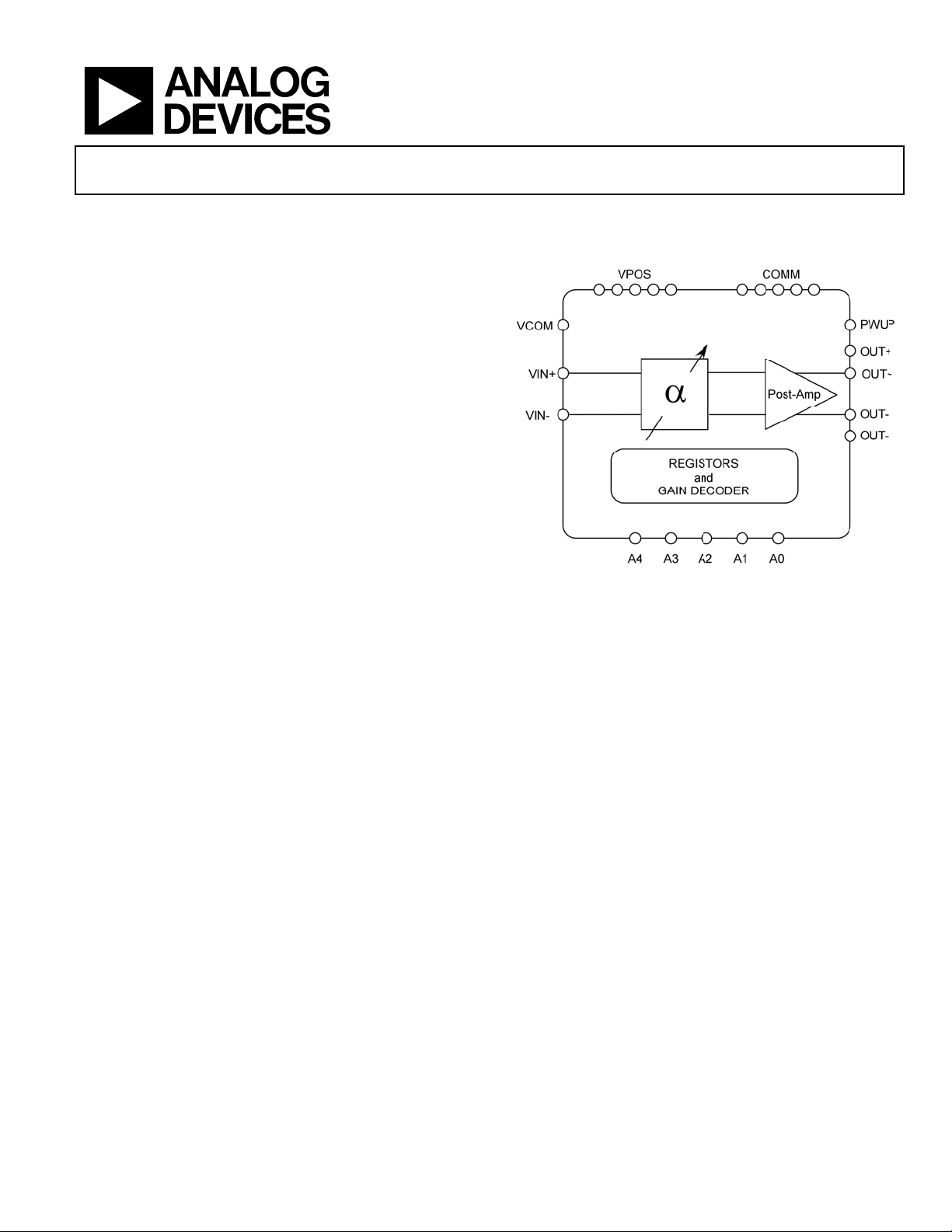
FUNCTIONAL BLOCK DIAGRAM
Figure 1.
Using a high speed SiGe process and incorporating proprietary
distortion cancellation techniques, the AD8375 achieves
50 dBm output IP3 at 140 MHz.
The AD8375 is powered on by applying the appropriate logic
level to the PWUP pin. The quiescent current of the AD8375 is
typically 130mA. When powered down, the AD8375 consumes
less than 5mA and offers excellent input to output isolation. The
gain setting is preserved when powered down.
Fabricated on an ADI’s high speed SiGe process, the AD8375
provides precise gain adjustment capabilities with good distortion
performance. The AD8375 amplifier comes in a compact,
thermally enhanced 4 x 4mm 24-lead LFCSP package and
operates over the temperature range of −40°C to +85°C.
Rev. PrB March 13, 2007
Information furnished by Analog Devices is believed to be accurate and reliable.
However, no responsibility is assumed by Analog Devices for its use, nor for any
infringements of patents or other rights of third parties that may result from its use.
Specifications subject to change without notice. No license is granted by implication
or otherwise under any patent or patent rights of Analog Devices. Trademarks and
registered trademarks are the property of their respective owners.
One Technology Way, P.O. Box 9106, Norwood, MA 02062-9106, U.S.A.
Tel: 781.329.4700 www.analog.com
Fax: 781.326.8703 © 2007 Analog Devices, Inc. All rights reserved.
Page 2

AD8375 Preliminary Technical Data
SPECIFICATIONS
VS = 5 V, T = 25°C, ZS = ZL = 150Ω at 100MHz, 2 V p-p differential output unless otherwise noted.
Tabl e 1.
Parameter Conditions Min Typ Max Unit
DYNAMIC PERFORMANCE
−3 dB Bandwidth V
Slew Rate
INPUT STAGE
Maximum Input Swing For linear operation (AV = 0dB)
Differential Input Resistance Differential
Common-Mode Input Voltage
CMRR Gain Code = 00000
GAIN
Amplifier Transconductance
Maximum Voltage Gain Gain Code = 00000
Minimum Voltage Gain
Gain Step Size From Gain Code 00000 to 11000
Gain Flatness
Gain Temperature Sensitivity Gain Code = 00000
Gain Step Response For VIN = 0.2V, Gain Code 10100 to 00000
OUTPUT STAGE
Output Voltage Swing At P1dB, Gain Code = 00000
Output impedance Differential
NOISE/HARMONIC PERFORMANCE
46 MHz Gain Code = 00000
Noise Figure
Second Harmonic V
Third Harmonic V
Output IP3 2 MHz spacing, +3 dBm per tone
Output 1 dB Compression Point
70 MHz Gain Code = 00000
Noise Figure
Second Harmonic V
Third Harmonic V
Output IP3 2 MHz spacing, +3 dBm per tone
Output 1 dB Compression Point
140 MHz Gain Code = 00000
Noise Figure
Second Harmonic V
Third Harmonic V
Output IP3 2 MHz spacing, +3 dBm per tone
Output 1 dB Compression Point
< 2 V p-p (5.2dBm)
OUT
690
TBD
MHz
V/nsec
Pins VIN+ and VIN-
TBD
150
2
TBD
V p-p
Ω
V
dB
-1
Ω
dB
dB
dB
dB
mdB/°C
Gain Code ≥11000
Gain Code = 00000 over 20% fractional
bandwidth for f
< 200MHz
C
0.58
-5.5
0.8
0.067 0.076
20
−4
1.0
TBD
TBD
TBD
-2.5
1.2
ns
Pins OUT+ and OUT-
10
5k//1
V p-p
Ω/pF
= 2 V p-p
OUT
= 2 V p-p
OUT
8.5
-94
-92
50
19
dB
dBc
dBc
dBm
dBm
= 2 V p-p
OUT
= 2 V p-p
OUT
8.5
-94
-92
50
19
dB
dBc
dBc
dBm
dBm
= 2 V p-p
OUT
= 2 V p-p
OUT
8.5
-86
-91
50
19
dB
dBc
dBc
dBm
dBm
Rev. PrB | Page 2 of 6
Page 3

Preliminary Technical Data AD8375
Parameter Conditions Min Typ Max Unit
200 MHz Gain Code = 00000
Noise Figure
Second Harmonic V
Third Harmonic V
Output IP3 2 MHz spacing, +3 dBm per tone
Output 1 dB Compression Point
POWER-INTERFACE
Supply Voltage
Quiescent Current per Channel
vs. Temperature −40°C ≤ TA ≤ +85°C
Power Down Current PWUP Low
vs. Temperature −40°C ≤TA ≤ +85°C
ENABLE INTERFACE
Enable Threshold
PWUP Input Bias Current
GAIN CONTROL INTERFACE Pins A0, A1, A2, A3, A4
V
IH
V
IL
Maximum Input Bias Current
= 2 V p-p
OUT
= 2 V p-p
OUT
thermal connection made to exposed paddle
under device
Pin PWUP
Minimum voltage to enable the device
Minimum voltage for a logic high 1.6
Maximum voltage for a logic low
8.5
4.5 5.5 V
-85
-88
50
18
130 140 mA
3 mA
0.5 nA
V
0.8
900 nA
165 mA
TBD mA
1.6 V
dB
dBc
dBc
dBm
dBm
Table 2. Gain-Code versus Voltage Gain Look-Up Table
5-Bit Binary Gain Code Voltage Gain (dB) 5-Bit Binary Gain Code Voltage Gain (dB)
00000 20 01101 7
00001 19 01110 6
00010 18 01111 5
00011 17 10000 4
00100 16 10001 3
00101 15 10010 2
00110 14 10011 1
00111 13 10100 0
01000 12 10101 -1
01001 11 10110 -2
01010 10 10111 -3
01011 9 11000 -4
01100 8 >11000 -4
Rev. PrB | Page 3 of 6
Page 4

AD8375 Preliminary Technical Data
ABSOLUTE MAXIMUM RATINGS
Parameter Rating
Supply Voltage, V
PWUP, A0, A1, A2, A3, A4 -0.6 to (V
Input Voltage, V
Internal Power Dissipation TBD mW
θJA (Exposed paddle soldered down) TBD°C/W
θJA (Exposed paddle not soldered down) TBD°C/W
θJC (At exposed paddle) TBD°C/W
Maximum Junction Temperature TBD°C
Operating Temperature Range –40°C to +85°C
Storage Temperature Range –65°C to +150°C
Lead Temperature Range
(Soldering 60 sec)
IN+
POS
,V
IN-
5.5 V
POS
-0.6 to +3.1V
TBD°C
+ 0.6V)
Stresses above those listed under Absolute Maximum
Ratings may cause permanent damage to the device.
This is a stress rating only; functional operation of the
device at these or any other conditions above those
listed in the operational sections of this specification is
not implied. Exposure to absolute maximum rating
conditions for extended periods may affect device
reliability.
ESD CAUTION
ESD (electrostatic discharge) sensitive device. Electrostatic charges as high as 4000 V readily accumulate on the
human body and test equipment and can discharge without detection. Although this product features
proprietary ESD protection circuitry, permanent damage may occur on devices subjected to high energy
electrostatic discharges. Therefore, proper ESD precautions are recommended to avoid performance
degradation or loss of functionality.
Rev. PrB | Page 4 of 6
Page 5

Preliminary Technical Data AD8375
PIN CONFIGURATION AND FUNCTIONAL DESCRIPTIONS
Figure 2. 24 Lead LFCSP
Table 3. Pin Function Descriptions
Pin No. Mnemonic Description
1 VCOM Common Mode Pin. Typically bypassed to ground using external capacitor.
2 VIN+ Voltage Input Positive.
3 VIN- Voltage Input Negative.
4 A4 The Most Significant Bit (MSB) for the 5-bit Gain Control Interface.
5 A3 MSB-1 for the Gain Control Interface.
6 A2 MSB-2 for the Gain Control Interface.
7 A1 LSB+1 for the Gain Control Interface.
8 A0 The Least Significant Bit (LSB) for the 5-bit Gain Control Interface.
9, 10,12, 13,
23
11, 14, 20,
21, 22, 24
15, 17 VOUT+ Positive Ouptut Pins (Open Collector). Require DC bias of +5V nominal.
16, 18 VOUT- Negative Ouptut Pins (Open Collector). Require DC bias of +5V nominal.
19 PWUP Chip Enable Pin.
VPOS Positive Supply Pins. Should be bypassed to Ground using suitable bypass capacitor.
COMM Device Common (DC Ground).
Rev. PrB | Page 5 of 6
Page 6

AD8375 Preliminary Technical Data
OUTLINE DIMENSIONS
Figure 2. 24-Lead LFCSP)
ORDERING GUIDE
Model Temperature Package Description Package Option
AD8375ACPZ-WP
AD8375ACPZ-REEL7
AD8375-EVALZ Evaluation Board
–40°C to +85°C
–40°C to +85°C
Waffle Pack, 24 Lead Frame Chip Scale
Package
7” Reel, 24 Lead Frame Chip Scale Package CP-24
CP-24
© 2007 Analog Devices, Inc. All rights reserved. Trademarks and
registered trademarks are the property of their respective owners.
PR06724-0-3/07(PrB)
Rev. PrB | Page 6 of 6
 Loading...