

Page 1
41 dB Range, 1 dB Step Size,
FEATURES
Dual independent digitally controlled VGA
Differential input and output
150 Ω differential input
Open-collector differential output
7.8 dB noise figure to 100 MHz @ maximum gain
HD2/HD3 better than 77 dBc for 1 V p-p differential output
−3 dB bandwidth of 150 MHz
41 dB gain range
1 dB step size ± 0.2 dB
Serial 8-bit bidirectional SPI control interface
Wide input dynamic range
Pin-programmable output stage
Power-down feature
Single 5 V supply: 106 mA per channel
32-lead LFCSP, 5 mm × 5 mm package
APPLICATIONS
Differential ADC drivers
CMTS upstream direct sampling receivers
CATV modem signal scaling
Generic RF/IF gain stages
Single-ended-to-differential conversion
Programmable Dual VGA
AD8372
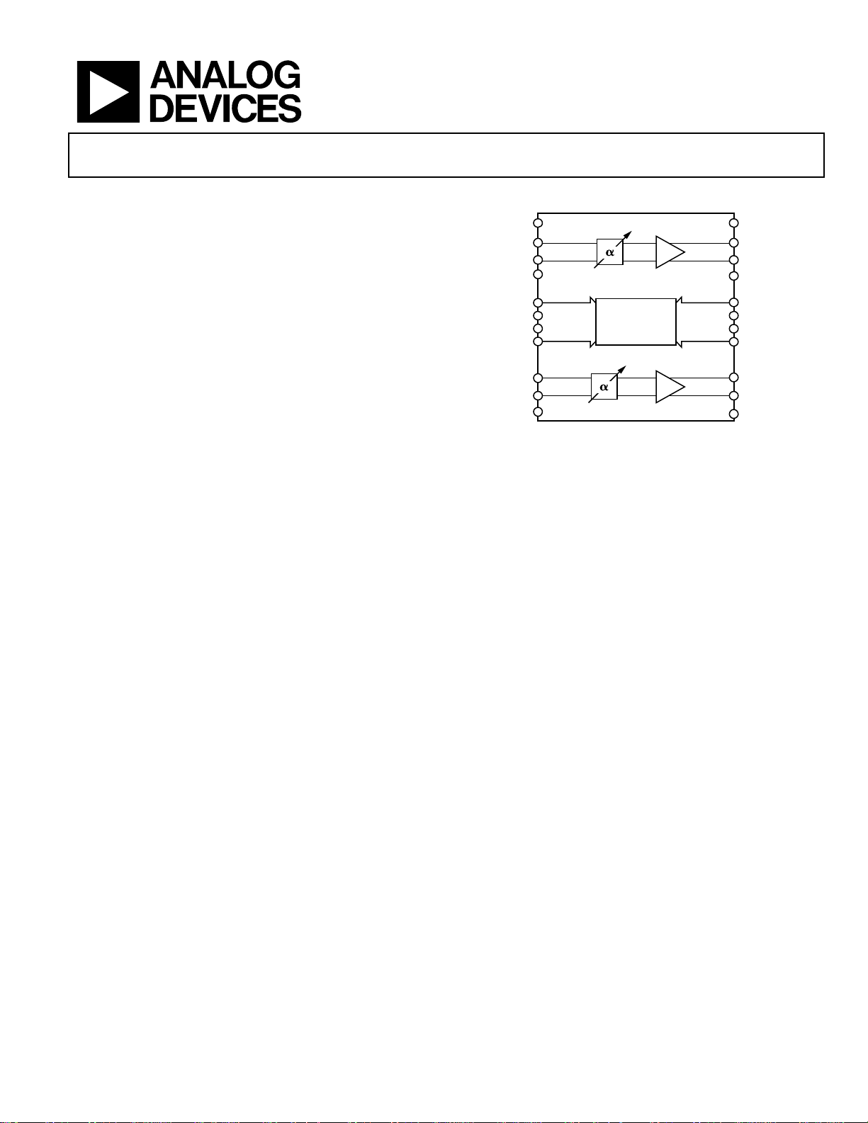
FUNCTIONAL BLOCK DIAGRAM
ENB1
IPC1
INC1
RXT2
CLK1
SDO1
SDI1
LCH1
IPC2
INC2
REF1
AD8372
CHANNEL 2
CHANNEL 1
REGISTERS
AND
GAIN DECODER
Figure 1.
POSTAMP
POSTAMP
REF2
OPC1
ONC1
RXT2
CLK2
SDO2
SDI2
LCH2
OPC2
ONC2
ENB2
07051-001
GENERAL DESCRIPTION
The AD8372 is a dual, digitally controlled, variable gain
amplifier that provides precise gain control, high IP3, and
low noise figure. The excellent distortion performance and
moderate signal bandwidth make the AD8372 a suitable
gain control device for a variety of multichannel receiver
applications.
For wide input dynamic range applications, the AD8372
provides a broad 41 dB gain range. The gain is programmed
through a bidirectional 4-pin serial interface. The serial interface consists of a clock, latch, data input, and data output lines
for each channel.
The AD8372 provides the ability to set the transconductance of
the output stage using a single external resistor. The RXT1 and
RXT2 pins provide a band gap derived stable reference voltage
of 1.56 V. Typically 2.0 k shunt resistors to ground are used to
set the maximum gain to a nominal value of 31 dB. The current
setting resistors can be adjusted to manipulate the gain and
distortion performance of each channel. This is a flexible
feature in applications where it is desirable to trade off distortion
performance for lower power consumption.
The AD8372 is powered on by applying the appropriate logic
level to the ENB1, ENB2 pins. When powered down, the AD8372
consumes less than 2.6 mA and offers excellent input-to-output
isolation. The gain setting is preserved when powered down.
Fabricated on an Analog Devices high frequency BiCMOS
process, the AD8372 provides precise gain adjustment capabilities
with good distortion performance. The quiescent current of the
AD8372 is typically 106 mA per channel. The AD8372 amplifier
comes in a compact, thermally enhanced 5 mm × 5 mm 32-lead
LFCSP package and operates over the temperature range of
−40°C to +85°C.
Rev. 0
Information furnished by Analog Devices is believed to be accurate and reliable. However, no
responsibility is assumed by Anal og Devices for its use, nor for any infringements of patents or ot her
rights of third parties that may result from its use. Specifications subject to change without notice. No
license is granted by implication or otherwise under any patent or patent rights of Analog Devices.
Trademarks and registered trademarks are the property of their respective owners.
One Technology Way, P.O. Box 9106, Norwood, MA 02062-9106, U.S.A.
Tel: 781.329.4700 www.analog.com
Fax: 781.461.3113 ©2007 Analog Devices, Inc. All rights reserved.
Page 2

AD8372
TABLE OF CONTENTS
Features .............................................................................................. 1
Applications....................................................................................... 1
Functional Block Diagram .............................................................. 1
General Description......................................................................... 1
Revision History ............................................................................... 2
Specifications..................................................................................... 3
Serial Control Interface Timing ................................................. 5
Absolute Maximum Ratings............................................................ 6
ESD Caution.................................................................................. 6
Pin Configuration and Function Descriptions............................. 7
REVISION HISTORY
11/07—Revision 0: Initial Version
Typical Perf or m an c e Charac t e r istics ..............................................8
Theory of Operation ...................................................................... 10
Single-Ended and Differential Signals..................................... 10
Passive Filter Techniques........................................................... 10
Digital Gain Control .................................................................. 10
Driving Analog-to-Digital Converters.................................... 10
Evaluation Board Schematic......................................................... 12
Outline Dimensions ....................................................................... 13
Ordering Guide .......................................................................... 13
Rev. 0 | Page 2 of 16
Page 3
AD8372
SPECIFICATIONS
VS = 5 V, T = 25°C, ZS = 150 Ω, ZL = 250 Ω at 35 MHz, 1 V p-p differential output, RXT1 = RXT2 = 2.0 k, unless otherwise noted.
Table 1.
Parameter Conditions Min Typ Max Unit
DYNAMIC PERFORMANCE
−3 dB Bandwidth V
INPUT STAGE Pin IPCI, Pin INC1, Pin IPC2, and Pin INC2
Maximum Input Swing at Each Input Pin 5 V p-p
Input Resistance Differential 150 Ω
Common-Mode Input Voltage 2.4 V
CMRR Gain code = 1x101010 (max gain) 55 dB
GAIN
Maximum Voltage Gain Gain code = 1x101010 32 dB
Minimum Voltage Gain Gain code = 1x000001 −9 dB
Gain Step Size From gain code 1x000001 to 1x101010 1.0 dB
Gain Step Accuracy From gain code 1x000001 to 1x101010 ±0.3 dB
Gain Flatness Gain code = 1x101010, from 5 MHz to 65MHz 0.7 dB
Gain Temperature Sensitivity Gain code = 1x101010 7.5 mdB/°C
Step Response For 6 dB gain step, 10% settling 20 ns
OUTPUT STAGE Pin OPCI, Pin ONC1, Pin OPC2, and Pin ONC2
Output Voltage Swing At P1dB, gain code = 1x101010 9 V p-p
Output Resistance Differential 3.5 kΩ
Channel Isolation
NOISE/HARMONIC PERFORMANCE
5 MHz Gain code = 1x101010 (max gain)
Noise Figure 7.8 dB
Second Harmonic 79 dBc
Third Harmonic 91 dBc
Output IP3 32 dBm
Output 1 dB Compression Point 18.2 dBm
35 MHz Gain code = 1x101010 (max gain)
Noise Figure 7.8 dB
Second Harmonic 79 dBc
Third Harmonic 87 dBc
Output IP3 35 dBm
Output 1 dB Compression Point 18.1 dBm
65 MHz Gain code = 1x101010 (max gain)
Noise Figure 7.9 dB
Second Harmonic 78 dBc
Third Harmonic 85 dBc
Output IP3 35 dBm
Output 1 dB Compression Point 17.9 dBm
85 MHz Gain code = 1x101010
Noise Figure 8.1 dB
Second Harmonic 77 dBc
Third Harmonic 85 dBc
Output IP3 35 dBm
Output 1 dB Compression Point 17.7 dBm
< 1 V p-p, C
OUT
Measured at differential output for differential input
applied to alternate channel
< 3pF 130 MHz
LOAD
55 dB
Rev. 0 | Page 3 of 16
Page 4
AD8372
Parameter Conditions Min Typ Max Unit
POWER INTERFACE
Supply Voltage 4.5 5.5 V
Quiescent Current per Channel
Thermal connection made to exposed paddle under
device
vs. Temperature −40°C ≤ TA ≤ +85°C 135 mA
Power-Down Current, Both Channels ENB1 and ENB2 low 1.2 mA
vs. Temperature −40°C ≤ TA ≤ +85°C 1.3 mA
ENABLE INTERFACE Pin ENB1 and Pin ENB2
Enable Threshold Minimum voltage to enable the device 0.8 V
ENB1, ENB2 Input Bias Current ENB1, ENB2 = 0 V 400 nA
GAIN CONTROL INTERFACE
Pin CLK1, Pin CLK2, Pin SDI1, Pin SDI2, Pin SDO1, Pin
SDO2, Pin LCH1, and Pin LCH2
V
IH
Minimum voltage for a logic high 2.4 V
Input Bias Current 400 nA
Serial Port Output Feedthrough
Worse-case feedthrough from CLK1, CLK2, SDI1,
SDI2, SDO1, SDO2, LCH1, LCH2 to OPC1 and ONC2,
or OPC2 and ONC2
106 mA
−60 dB
Table 2. Gain Code vs. Voltage Gain Look-Up Table
8-Bit Binary Gain Code
1
Voltage Gain (dB)
RW DC 000000 < −60
RW DC 000001 −9
RW DC 000010 −8
RW DC 000011 −7
RW DC 000100 −6
RW DC 000101 −5
RW DC 000110 −4
RW DC 000111 −3
RW DC 001000 −2
RW DC 001001 −1
RW DC 001010 0
RW DC 001011 +1
RW DC 001100 +2
RW DC 001101 +3
RW DC 001110 +4
RW DC 001111 +5
RW DC 010000 +6
RW DC 010001 +7
RW DC 010010 +8
RW DC 010011 +9
RW DC 010100 +10
RW DC 010101 +11
1
RW is the Read/Write bit, RW = 0 for read mode, RW = 1 for write mode. DC is
the Don’t Care bit.
8-Bit Binary Gain Code
1
Voltage Gain (dB)
RW DC 010110 +12
RW DC 010111 +13
RW DC 011000 +14
RW DC 011001 +15
RW DC 011010 +16
RW DC 011011 +17
RW DC 011100 +18
RW DC 011101 +19
RW DC 011110 +20
RW DC 011111 +21
RW DC 100000 +22
RW DC 100001 +23
RW DC 100010 +24
RW DC 100011 +25
RW DC 100100 +26
RW DC 100101 +27
RW DC 100110 +28
RW DC 100111 +29
RW DC 101000 +30
RW DC 101001 +31
RW DC 101010 +32
RW DC 101011 < −60
Rev. 0 | Page 4 of 16
Page 5
AD8372
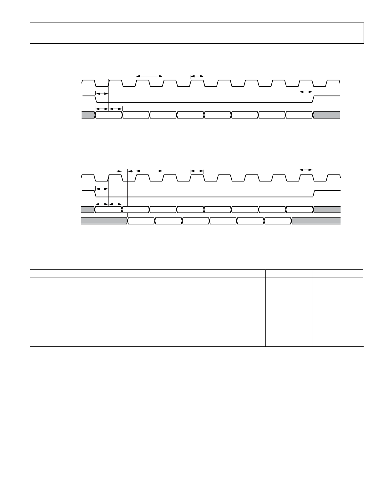
SERIAL CONTROL INTERFACE TIMING
t
CLK
CLK1 OR CLK2
LCH1 OR LCH2
SDI1 OR SDI2
NOTES
1. THE FI RST SDI BIT DETERMINES WHETHER THE PART IS WRITING T O OR READING FROM THE INTERNAL GAIN WORD REGI STER. F OR A
WRITE O PERATION, THE FI RST BIT S HOULD BE A HIG H LOGIC LEVEL, FOR A READ OPERATION THE FIRST BI T SHOULD BE A LOGIC 1.
THE GAIN W ORD BIT IS THEN REGISTERED INTO THE SDI PI N ON THE NEXT RISING CL OCK.
t
LS
t
t
DH
DS
DON'T CAREWRITE BIT LSB LSB + 1 LSB + 2 MSB – 2 MSB – 1 MSB
Figure 2. Write Mode Timing Diagram
t
CLK
DCDCREAD BIT DC DC DC DC DC
CLK1 OR CLK2
LCH1 OR LCH2
SDI1 OR SDI2
t
D
t
LS
t
t
DH
DS
t
PW
t
LH
07051-003
t
t
PW
LH
SDO1 OR SDO2
NOTES
1. THE GAI N WORD BIT IS UPDATED AT THE SDO PIN ON THE FAL LING CL OCK EDGE.
LSB LSB + 1 LSB + 2 MSB – 2 MSB – 1 MSB
07051-004
Figure 3. Read Mode Timing Diagram
Table 3. Serial Programming Timing Parameters
Parameter Min Unit
Clock Pulse Width (tPW) 10 ns
Clock Period (tCK) 20 ns
Write Mode
Setup Time Data vs. Clock (tDS) 0.0 ns
Hold Time Data vs. Clock (tDH) 1.6 ns
Setup Time Latch vs. Clock (tLS) −1.8 ns
Hold Time Latch vs. Clock (tLH) 2.0 ns
Read Mode
Clock to Data Out (tD) 4.5 ns
Rev. 0 | Page 5 of 16
Page 6

AD8372
ABSOLUTE MAXIMUM RATINGS
Table 4.
Parameter Rating
Supply Voltage, VS 5.5 V
+ 500 mV
ENB1, ENB2, SDI1, SDI2, SDO1, SDO2,
V
S
CLK1, CLK2, LCH1, LCH2
Differential Input Voltage, V
V
− V
IPC2
INC2
IPC1
− V
INC1
V p-p
,
Internal Power Dissipation 1.4 W
θJA (Exposed Paddle Soldered Down) 34.6°C/W
θJC (At Exposed Paddle) 3.6°C/W
1, 2
2
Maximum Junction Temperature 150°C
Operating Temperature Range −40°C to +85°C
Storage Temperature Range −65°C to +150°C
1
Still air.
2
All values are modeled using a standard 4-layer JEDEC test board with the
pad soldered to the board and thermal vias in the board.
Stresses above those listed under Absolute Maximum Ratings
may cause permanent damage to the device. This is a stress
rating only; functional operation of the device at these or any
other conditions above those indicated in the operational
section of this specification is not implied. Exposure to absolute
maximum rating conditions for extended periods may affect
device reliability.
ESD CAUTION
Rev. 0 | Page 6 of 16
Page 7

AD8372
PIN CONFIGURATION AND FUNCTION DESCRIPTIONS
AVS1
ENB1
AGD1
RXT1
REF1
IPC1
INC1
DGD1
25
26
27
28
29
31
30
32
1DVS1
2LCH1
3SDI1
4CLK1
5CLK2
6SDI2
7LCH2
8DVS2
PIN 1
INDICATOR
AD8372
TOP VIEW
(Not to S cale)
9
11
12
10
C2
IPC2
IN
REF2
DGD2
13
RXT2
24 OPC1
23 ONC1
22 AGD1
21 SDO1
20 SDO2
19 AGD2
18 ONC2
17 OPC2
14
15
16
VS2
A
ENB2
AGD2
Figure 4. Pin Configuration
Table 3. Pin Function Descriptions
Pin No. Mnemonic Description
1 DVS1 Digital Supply Pin for Channel 1
2 LCH1 Latch Input for Channel 1
3 SDI1 Serial Data Input for Channel 1
4 CLK1 Clock Input for Channel 1
5 CLK2 Clock Input for Channel 2
6 SDI2 Serial Data Input for Channel 2
7 LCH2 Serial Data Input for Channel 2 Latch Input for Channel 2
8 DVS2 Digital Supply Pin for Channel 2
9 DGD2 Digital Ground for Channel 2
10 INC2 Negative Input for Channel 2
11 IPC2 Positive Input for Channel 2
12 REF2 Reference Voltage for Channel 2
13 RXT2 External Bias Setting Resistor Connection for Channel 2
14 AGD2 Analog Ground for Channel 2
15 ENB2 Chip Enable Pin for Channel 2
16 AVS2 Analog Supply Pin for Channel 2
17 OPC2 Positive Output for Channel 2
18 ONC2 Negative Output for Channel 2
19 AGD2 Analog Ground for Channel 2
20 SDO2 Serial Data Output for Channel 2
21 SDO1 Serial Data Output for Channel 1
22 AGD1 Analog Ground for Channel 1
23 ONC1 Negative Output for Channel 1
24 OPC1 Positive Output for Channel 1
25 AVS1 Analog Supply Pin for Channel 1
26 ENB1 Chip Enable Pin for Channel 1
27 AGD1 Analog Ground for Channel 1
28 RXT1 External Bias Setting Resistor Connection for Channel 1
29 REF1 Reference Voltage for Channel 1
30 IPC1 Positive Input for Channel 1
31 INC1 Negative Input for Channel 1
32 DGD1 Digital Ground for Channel 1
07051-002
Rev. 0 | Page 7 of 16
Page 8

AD8372
–
TYPICAL PERFORMANCE CHARACTERISTICS
VS = 5 V, TA = 25°C, ZS = 150 , ZL = 250 Ω, 1 V p-p differential output, both channels enabled, unless otherwise noted.
40
20
30
20
10
0
VOLTAGE GAIN (dB)
–10
–20
–30
1M 10M 100M 1G
FREQUENCY (Hz)
Figure 5. Gain vs. Frequency by Gain Code (All Codes),
Differential In, Differential Out
60
–65
–70
–75
–80
–85
–90
HARMONIC DISTO RTION (d Bc)
–95
–100
0 102030405060708090
Figure 6. 2
HD2
HD3
FREQUENCY (MHz)
nd
and 3rd Harmonic Distortion
19
+25°C
18
+85°C
–40°C
17
16
OUTPUT REFERRED P1dB (dBm)
15
0 102030405060708090
07051-005
FREQUENCY (MHz)
07051-008
Figure 8. P1dB, Maximum Gain
180
160
140
120
100
80
RESISTANCE (Ω)
60
40
20
0
0
07051-006
50000000
100000000
FREQUENCY (MHz)
150000000
200000000
250000000
9
8
7
6
5
4
3
2
1
0
300000000
CAPACIT ANCE (pF )
07051-009
Figure 9. Input Equivalent Parallel Impedance
100
90
80
70
60
50
40
OIP2/OIP3 (dBm)
30
20
10
0
0 102030405060708090
OIP3 – A
OIP2 – A
= 10
V
= 32
V
OIP2 – A
FREQUENCY (MHz)
= 10
V
OIP2 – A
OIP3 – AV = 32
OIP3 – A
Figure 7. OIP2 and OIP3
V
= –9
V
= –9
07051-007
70
60
50
40
30
CMRR (dB)
20
10
0
0 102030405060708090100
FREQUENCY (MHz)
Figure 10. CMRR vs. Frequency
07051-010
Rev. 0 | Page 8 of 16
Page 9

AD8372
50
45
40
35
30
25
20
NOISE FIGURE (dB)
15
10
5
0
0
20 40 60 80 100 120 140 160 180 200
Figure 11. Noise Figure vs. Frequency
AV = 0dB
AV = 10dB
= 20dB
A
V
A
= 32dB
V
FREQUENCY (MHz)
20ns/DIV
07051-012
07051-011
Figure 13. AD8372 Response to 6 dB Step Change in Gain (Gain Register
Setting 36 to Setting 42); Falling Edge Shown is Serial Clock Input Edge
0
–10
–20
–30
–40
(dB)
–50
–60
–70
–80
–90
1M 10M 100M 1G
FREQUENCY (Hz)
Figure 12. Isolation, Input to Opposite Output at Maximum Gain
(To calculate output to output gain, subtract 29 dB from this plot)
07051-013
Rev. 0 | Page 9 of 16
Page 10

AD8372
THEORY OF OPERATION
The AD8372 is a dual differential variable gain amplifier. Each
amplifier consists of a 150 digitally controlled 6 dB attenuator
followed by a 1 dB vernier and a fixed gain transconductance
amplifier.
The differential output on each amplifier consists of a pair of
open-collector transistors. It is recommended that each opencollector output be biased to +5 V with a high value inductor.
A 33 H inductor, such as the Coilcraft® 1812LS-333XJL, is an
excellent choice for this component. A 250 resistor should be
placed across the differential outputs to provide a current-tovoltage conversion and as a source impedance for passive
filtering, post AD8372.
The gain for each side is based on a 250 differential load and
varies as the R
Gain = 20log(R
Gain = 10log(R
changes per the following equations:
LOAD
/250), for voltage gain
LOAD
/250), for power gain
LOAD
The dependency of the gain on the load is due to the opencollector output stage that is biased using external chokes. The
inductance of the chokes and the resistance of the load determine the low frequency pole of the amplifier. The high frequency
pole is set by the parasitic capacitance of the chokes and outputs
in parallel with the output resistance.
The total supply current of 106 mA per side consists of 70 mA
for the combined outputs and about 36 mA through the power
supply pins. Each side has an external resistor (R
) to ground
EXT
to set the transconductance of the output stage. For optimum
distortion, 106 mA total current per side is recommended,
making the R
value about 2.0 k. Each side has a 2.4 V
EXT
reference pin and that same common-mode voltage appears on
the inputs. This reference should be decoupled using a 0.1 F
capacitor. The part can be powered down to less than 2.6 mA by
setting the ENB pin low for the appropriate side.
The noise figure of the AD8372 is 7.8 dB at maximum gain and
increases as the gain is reduced. The increase in noise figure is
equal to the reduction in gain.
The linearity of the part measured at the output is first-order
independent of the gain setting.
Layout considerations should include minimizing capacitance
on the outputs by avoiding ground planes under the chokes, and
equalizing the output line lengths for phase balance.
SINGLE-ENDED AND DIFFERENTIAL SIGNALS
The AD8372 was designed to be used by applying differential
signals to the inputs and using the differential output drive of
the device to drive the next device in the signal chain. The
excellent distortion performance of the AD8372 is due
primarily to the use of differential signaling techniques to
cancel various distortion components in the device. In addition,
all ac characterization was done using differential signal paths.
Using this device with either the input or the output in a singleended circuit significantly degrades the overall performance of
the AD8372.
PASSIVE FILTER TECHNIQUES
The AD8372 has a 100 differential input impedance. For
optimal performance, the differential output load should be
250 . When designing passive filters around the AD8372,
these impedances must be taken into account.
DIGITAL GAIN CONTROL
The digital gain control interface consists of four pins: SDI,
SDO, CLK, and LATCH. The interface is active when the
LATCH pin is shifted low. Gain words are written into the
AD8372 via the SDI pin, and read back from the SDO pin. The
first bit clocked into the data input pin determines whether the
interface is in write or read mode. The second bit is a don’t care
bit, while the remaining six bits program the gain. In read
mode, the SDO pin clocks out the 6-bit gain word, LSB to MSB.
The gain can be programmed between −9 dB and 32 dB in 1 dB
steps. Timing details are given in
gain code table is given in
Figure 2 and Figure 3. The
Tabl e 3 .
DRIVING ANALOG-TO-DIGITAL CONVERTERS
The AD8372 was designed with the intention of driving high
speed, high dynamic range ADCs. The circuit in
represents a simplified front end of one-half of the AD8372 dual
VGA driving an
AD9445 14-bit, 125 MHz analog-to-digital
converter. The input of the AD8372 is driven differentially
using a 1:3 impedance ratio transformer, which also matches
the 150 input resistance to a 50 source. The open-collector
outputs are biased through the 33 H inductors and are accoupled from the 142 load resistors that, in parallel with the
2 k input resistance of the ADC, provide a 250 load for gain
accuracy. The ADC is ac-coupled from the 142 resistors to
negate a dc affect on the input common-mode voltage of the
AD9445. Including the series 33 resistors improves the
isolation of the AD8372 from the switching currents caused by
the ADC input sample and hold. The AD9445 represents a 2 k
differential load and requires a 2 V p-p signal when VREF = 1 V
for a full-scale output. This circuit provides variable gain,
isolation, and source matching for the AD9445. Using this
circuit with the AD8372 in a gain of 32 dB (maximum gain), an
SFDR performance of 74.5 dBc is achieved at 85 MHz. See
Figure 15.
Figure 14
Rev. 0 | Page 10 of 16
Page 11

AD8372
V
5V
0.1µF
1:3
50Ω
AC
0.1µF
½
AD8372
VGA
ENA1
SD01
CKL1
5
33µH
142Ω
0.1µF
0.1µF
33Ω
VIN+
AD9445
14-BIT ADC
VIN–
0.1µF
142Ω
33Ω
0.1µF
33µH
5V
14
07051-018
Figure 14. AD8372 Driving an AD9445 ADC
0
FUND: –1.053dBF S
–10
2ND: –74.55dBc
3RD: –86.45dBc
–20
4TH: –91.35dBc
–30
5TH: –89.57dBc
6TH: –91.15dBc
–40
–50
–60
–70
–80
(dBc)
–90
–100
–110
–120
–130
–140
–150
5 6
ENCODE: 105MHz
SAMPLES: 32768
ANALOG: 19. 8766MHz
5.25 10.50 15.75 21.00 26.25 31.50 36.75 42.00 47. 25 52.500
Figure 15. 74.5 dB SFDR Performance of the AD8372 Driving the AD9445 ADC
1
NOISE FLOOR: –101. 3dB
4
FREQUENCY (MHz )
SNR: 58.12dBc
SNRFS: 59.18dBc
THD: –73.99dBc
SINAD: 58.01dBc
SFDR: 74.73dBc
WO SPUR: –85.5dBc
2
3
FUND LEAK: 100
HARM LEAK: 3
DC LEAK: 6
07051-019
Rev. 0 | Page 11 of 16
Page 12

AD8372
EVALUATION BOARD SCHEMATIC
07051-014
OPC2
ONC1
OPC1
AGND
TBD
R29
R0603
4
T4
AGND
0
R44
R0603
C17
0.1UF
C0603
R21
100 OHMS
R0603
TBD
R35
0.1UF
C0603
100 OHMS
C0603
1NF
0
R16
R0603
50 OHMS
50 OHMS
6
SEC PRI
123
0
R0603
C11
H1-15
H1-15
AGND
C16
AGND
C15
R0603
0.1UF
C0603
TBD
R30
AGND
AGND
R46
0
R43
R0603
100 OHMS
AGND
R0603
R36
TBD
0.1UF
C0603
C18
100 OHMS
1812
33UH
L2
1812
33UH
R22
L1
100 OHMS
0
R23
R0603
0
R0603
100 OHMS
0
0.1UF
C0603
0
R0603
SDO1
100 OHMS
100 OHMS
R14
H1-15
10K
TBD
R47
R0603
H1-7
R18
R0603
W2
AGND
R2
R0603
2.74K
AGNDAGND
R32
AGND
IPC1
AGND
INC1
TBD
R12
TBD
R0603
50 OHMS
75 OHMS
T2
SEC PRI
146
R15
TBD
2
R0603
3
R0603 R0603
R31
TBD
50 OHMS
75 OHMS
AGND
0.1UF
C0603
C32
AGND
0.1UF
C0603
C26
R40
TBD
R0603R0603
0.1UF
C0603
C27
AGND
0.1UF
C0603
C25
R39
TBD
2526272829
AGND
303132
DGND
75 OHMS
75 OHMS
AGND
AGND
SDO1
SDO2
17181922021222324
2PCO2SVD
ONC2
AGD2
SDO2
SDO1
AGD1
ONC1
OPC1
AVS1
ENB1
AGD1
RXT1
REF1
Z1
IPC1
AD8372
INC1
DGD1
DVS1
1
SDI1
LCH1
3
CLK2
CLK1
SDI2
45678
LCH2
ONC2
AGND
TBD
R28
50 OHMS
R0603
4
T3
321
100 OHMS
R0603
R25
R0603
R26
R0603
C28
R37
TBD
0.1UF
C0603
1812
33UH
L4
1812
33UH
0
R24
L3
0
R0603
AGND
C10
TBD
C0603
H1-6
AVS2
ENB2
ADG2
AGND
RXT2
REF2
IPC2
INC2
10 11 12 13 14 15 16
DGD2
9
DGND
75 OHMS
75 OHMS
50 OHMS
R0603
TBD
R27
6
SEC PRI
0
R0603
R0603
R38
TBD
C29
H1-15
AGND
AGND
C14
0.1UF
C0603
R45
0
R0603
AGND
100 OHMS
R49
SSVDDV
H1-13
0
R0603
H1-15
SDO2H1-12
0
R13
R0603
C9
TBD
C0603
H1-7
C0603
AGND
C12
R17
C13
1NF
0.1UF
C0603
0
R3
R0603
10K
R48
R0603
W1
AGND
R1
R0603
2.74K
AGND
0.1UF
C0603
C19
AGND
0.1UF
C0603
C24
R42
AGND
0.1UF
C23
0.1UF
C0603
C22
R41
R0603
TBD
R33
TBD
75 OHMS
C0603
TBD
R0603 R0603
T1
SECPR I
146
2
3
TBD
R34
AGND
R20
50 OHMS
R19
R0603
AGND
50 OHMS
75 OHMS
DGND
3528
10UF
C34
TESTLO OP
ORANGE
H1-15
L6
C1206
TBD
RED
TESTLO OP
H1-1
C33
10UF
3528
AGND
DGND
DGNDAGND
L5
C1206
TBD
AGND
14P1
15P1
16P1
17P1
18P1
AGND
H1-15
TBD
R0603
H1-13
H1-4
H1-3
H1-5
H1-6
5P1
4P1
3P1
2P1
1P1
19P1
AGND
20P1
21P1
22P1
23P1
24P1
25P1
H1-11
H1-12
H1-9
H1-10
8P1
7P1
6P1
H1-12
H1-6
13P1
12P1
11P1
9P1
10P1
INC2
H1-14
H1-4
H1-5
H1-6
H1-13
TBD
R0603
AGND
TBD
R0603
AGND
B11P2
B12P2
B13P2
B15P2
B14P2
IPC2
AGND
H1-12
H1-6
H1-9
H1-1
AGND
H1-16
H1-15
H1-3
B20P2
B19P2
B18P2
B17P2
B16P2
H1-8
H1-12
H1-10
H1-11
H1-7
B1P2
B2P2
B3P2
B4P2
B5P2
B6P2
B7P2
B8P2
B9P2
B10P2
DGND
W3
C0603
TBD
C8
R0603
0
R11
0.1UF
C0603
C21
C0603
TBD
DGND
C6
R0603
0
R9
DGND DGND
R10
DGND
W4W5W6W7W8
C0603
TBD
DGND
C7
R0603
0
R8
DGND
C0603
C5
TBD
DGND
R0603
0
R7
DGND
C0603
C4
TBD
DGND
R0603
R6
0
DGND
C0603
TBD
DGND
C3
R0603
0
R5
AD8372 CHAR BD
H1-1
H1-3
H1-4
H1-5
H1-11
H1-10
DGND
H1-14
H1-4
H1-16
H1-15
H1-3
H1-5
H1-6
H1-13
C0603
TBD
C2
R0603
0
H1-9
C0603
DGND
C1
TBD
R0603
0
R4
0.1UF
C0603
C20
DGND DGND
H1-1
A13P2
A15P2
A11P2
A1P2
A16P2
A12P2
A14P2
A17P2
A18P2
A19P2
A20P2
H1-1
H1-9
A2P2
A3P2
A4P2
A5P2
H1-8
H1-12
H1-10
H1-11
H1-7
A6P2
A7P2
A8P2
A9P2
A10P2
Figure 16. AD8372 Evaluation Board Schematic
Rev. 0 | Page 12 of 16
Page 13

AD8372
OUTLINE DIMENSIONS
0.08
0.60 MAX
25
24
EXPOSED
PAD
(BOTTOM VIEW)
17
16
32
1
8
9
3.50 REF
PIN 1
INDICATOR
3.25
3.10 SQ
2.95
0.25 MIN
5.00
PIN 1
INDICATOR
1.00
0.85
0.80
12° MAX
SEATING
PLANE
BSC SQ
TOP
VIEW
0.80 MAX
0.65 TYP
0.30
0.23
0.18
COMPLIANT TO JEDEC STANDARDS MO-220-VHHD-2
4.75
BSC SQ
0.20 REF
0.05 MAX
0.02 NOM
0.60 MAX
0.50
BSC
0.50
0.40
0.30
COPLANARITY
Figure 17. 32-Lead Lead Frame Chip Scale Package [LFCSP_VQ]
5 mm × 5 mm Body, Very Thin Quad
(CP-32-2)
Dimensions shown in millimeters
ORDERING GUIDE
Temperature
Model
Range
Package Description
AD8372ACPZ-WP1−40°C to +85°C 32-Lead Lead Frame Chip Scale Package [LFCSP_VQ], Waffle Pack CP-32-2
AD8372ACPZ-R7
AD8372-EVALZ
1
Z = RoHS Compliant Part.
1
−40°C to +85°C 32-Lead Lead Frame Chip Scale Package [LFCSP_VQ], 7” Reel CP-32-2 1,500
1
Evaluation Board
Package
Option
Ordering
Quantity
Rev. 0 | Page 13 of 16
Page 14

AD8372
NOTES
Rev. 0 | Page 14 of 16
Page 15

AD8372
NOTES
Rev. 0 | Page 15 of 16
Page 16

AD8372
NOTES
©2007 Analog Devices, Inc. All rights reserved. Trademarks and
registered trademarks are the property of their respective owners.
D07051-0-11/07(0)
Rev. 0 | Page 16 of 16
 Loading...