45 dB Digitally Controlled VGA
LF to 600 MHz
FEATURES
Digitally Controlled Variable Gain in 3 dB Steps
–5 dB to +40 dB (R
–10 dB to +35 dB (R
Less than 0.2 dB Flatness over a
= 1 k⍀)
L
= 200 ⍀)
L
+20 MHz Bandwidth
up to 380 MHz
4-Bit Parallel or 3-Wire Serial Interface
Differential 200 ⍀ Input and Output Impedance
Single 3.0 V–5.5 V Supply
Draws 37 mA at 5 V
Power-Down <1 mA Maximum
APPLICATIONS
Cellular/PCS Base Stations
IF Sampling Receivers
Fixed Wireless Access
Wireline Modems
Instrumentation
PRODUCT DESCRIPTION
The AD8369 is a high performance digitally controlled variable
gain amplifier (VGA) for use from low frequencies to a –3 dB
frequency of 600 MHz at all gain codes. The AD8369 delivers
excellent distortion performance: the two-tone, third-order
intermodulation distortion is –69 dBc at 70 MHz for a 1 V p-p
composite output into a 1 kW load. The AD8369 has a nominal
noise figure of 7 dB when at maximum gain, then increases with
decreasing gain.
Output IP3 is +19.5 dBm at 70 MHz into a
1 kW load and remains fairly constant over the gain range.
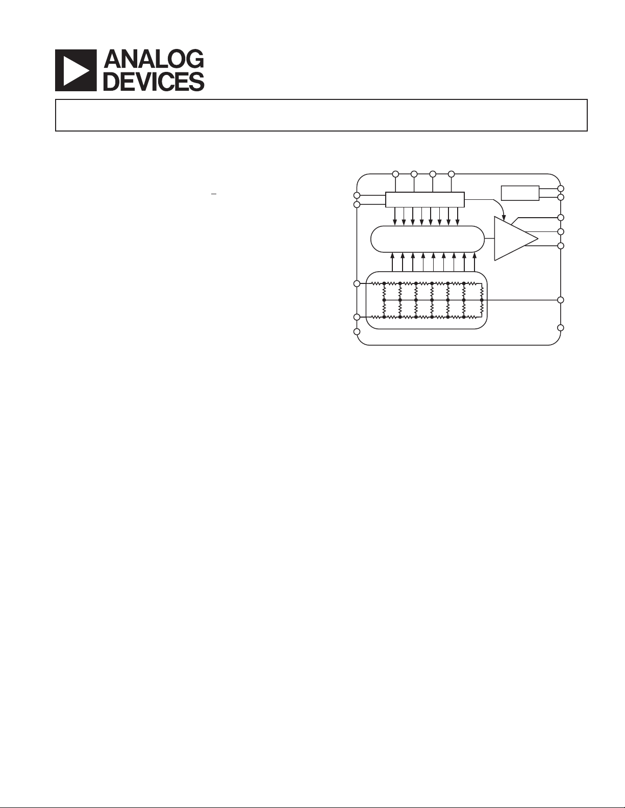
The signal input is applied to pins INHI and INLO. Variable gain
is achieved via two methods. The 6 dB gain steps are implemented
using a discrete X-AMP
®
structure, in which the input signal is
progressively attenuated by a 200 W R-2R ladder network that
also sets the input impedance; the 3 dB steps are implemented at
the output of the amplifier. This combination provides very
accurate 3 dB gain steps over a span of 45 dB. The output impedance is set by on-chip resistors across the differential output pins,
AD8369
*
FUNCTIONAL BLOCK DIAGRAM
BIT3 BIT0BIT2 BIT1
DENB
SENB
INHI
INLO
COMM
GAIN CODE DECODE
Gm CELLS
3dB STEP
BIAS
VPOS
PWUP
FILT
OPHI
OPLO
CMDC
COMM
OPHI and OPLO. The overall gain depends upon the source
and load impedances due to the resistive nature of the input and
output ports.
Digital control of the AD8369 is achieved using either a serial or
a parallel interface. The mode of digital control is selected by
connecting a single pin (SENB) to ground or the positive supply. Digital control pins can be driven with standard CMOS
logic levels.
The AD8369 may be powered on or off by a logic level applied
to the PWUP pin. For a logic high, the chip powers up rapidly
to its nominal quiescent current of 37 mA at 25ºC. When low,
the total dissipation drops to less than a few milliwatts.
The AD8369 is fabricated on an Analog Devices proprietary, high
performance 25 GHz silicon bipolar IC process and is available
in a 16-lead TSSOP package for the industrial temperature range
of –40∞C to +85∞C. A populated evaluation board is available.
*Patents Pending
REV. 0
Information furnished by Analog Devices is believed to be accurate and
reliable. However, no responsibility is assumed by Analog Devices for its
use, nor for any infringements of patents or other rights of third parties that
may result from its use. No license is granted by implication or otherwise
under any patent or patent rights of Analog Devices. Trademarks and
registered trademarks are the property of their respective companies.
One Technology Way, P.O. Box 9106, Norwood, MA 02062-9106, U.S.A.
Tel: 781/329-4700 www.analog.com
Fax: 781/326-8703 © 2002 Analog Devices, Inc. All rights reserved.

(VS = 5 V, T = 25ⴗC, RS = 200 ⍀, RL = 1000 ⍀, Frequency = 70 MHz, at maximum gain,
AD8369–SPECIFICATIONS
unless otherwise noted.)
Parameter Conditions Min Typ Max Unit
OVERALL FUNCTION
Frequency Range 3 dB Bandwidth LF* 600 MHz
GAIN CONTROL INTERFACE
Voltage Gain Span 45 dB
Maximum Gain All bits high (1 1 1 1) 40 dB
Minimum Gain All bits low (0 0 0 0) –5 dB
Gain Step Size 3dB
Gain Step Accuracy
Over entire gain range, with respect to 3 dB step
± 0.05 dB
Gain Step Response Time Step = 3 dB, settling to 10% of final value 30 ns
INPUT STAGE
Input Resistance From INHI to INLO 200 W
From INHI to COMM, from INLO to COMM 100 W
Input Capacitance From INHI to INLO 0.1 pF
From INHI to COMM, from INLO to COMM 1.1 pF
Input Noise Spectral Density 2 nV/÷Hz
Input Common-Mode DC Voltage Measured at pin CMDC 1.7 V
Maximum Linear Input |V
INHI
– V
| at Minimum Gain 2.2 V
INLO
OUTPUT STAGE
Output Resistance From OPHI to OPLO 200 W
From OPHI to COMM, from OPLO to COMM 100 W
Output Capacitance From OPHI to OPLO 0.25 pF
From OPHI to COMM, from OPLO to COMM 1.5 pF
Common-Mode DC Voltage No input signal V
/2 V
S
Slew Rate Output step = 1 V 1200 V/ms
POWER INTERFACE
Supply Voltage 3.0 5.5 V
Quiescent Current PWUP high 37 42 mA
vs. Temperature –40∞C £ T
£ 85∞C52mA
A
Disable Current PWUP low 400 750 mA
vs. Temperature –40∞C £ TA £ 85∞C1mA
POWER UP INTERFACE Pin PWUP
Enable Threshold 1.0 V
Disable Threshold 2.2 V
Response Time Time delay following low to high transition 7 ms
on PWUP until output settles to within 10%
of final value
Input Bias Current PWUP = 5 V 160 mA
DIGITAL INTERFACE
Pins SENB, BIT0, BIT1, BIT2, BIT3,
and DENB
Low Condition 2.0 V
High Condition 3.0 V
Input Bias Current Low input 150 mA
Frequency = 10 MHz
Voltage Gain 40.5 dB
Gain Flatness Within ± 10 MHz of 10 MHz
+0.05* dB
Noise Figure 7.0 dB
Output IP3 f1 = 9.945 MHz, f2 = 10.550 MHz +22 dBV rms
+22 dBm
IMD
3
Harmonic Distortion Second-Order, V
f1 = 9.945 MHz, f2 = 10.550 MHz
V
– V
OPHI
Third-Order, V
= 1 V p-p composite –74 dBc
OPLO
OPHI
OPHI
– V
– V
= 1 V p-p –72 dBc
OPLO
= 1 V p-p –71 dBc
OPLO
P1dB For ± 1dB deviation from linear gain +3 dBV rms
+3 dBm
*The low frequency high-pass corner is determined by the capacitor on pin FILT, C
. See the Theory of Operation section for details.
FILT
REV. 0–2–

SPECIFICATIONS (Continued)
AD8369
Parameter Conditions Min Typ Max Unit
Frequency = 70 MHz
Voltage Gain 40.5 dB
Gain Flatness Within ± 20 MHz of 70 MHz ± 0.1 dB
Noise Figure 7.0 dB
Output IP3 f1 = 69.3 MHz, f2 = 70.7 MHz +19.5 dBV rms
+19.5 dBm
IMD
3
Harmonic Distortion Second-Order, V
f1 = 69.3 MHz, f2 = 70.7 MHz
– V
V
OPHI
Third-Order, V
= 1 V p-p composite –69 dBc
OPLO
OPHI
OPHI
– V
– V
= 1 V p-p –68 dBc
OPLO
= 1 V p-p –64 dBc
OPLO
P1dB For ± 1dB deviation from linear gain +3 dBV rms
+3 dBm
Frequency = 140 MHz
Voltage Gain 40.0 dB
Gain Flatness Within ± 20 MHz of 140 MHz ± 0.10 dB
Noise Figure 7.0 dB
Output IP3 f1 = 139.55 MHz, f2 = 140.45 MHz +17 dBV rms
+17 dBm
IMD
3
Harmonic Distortion Second-Order, V
f1 = 139.55 MHz, f2 = 140.45 MHz
– V
V
OPHI
Third-Order, V
= 1 V p-p composite –64 dBc
OPLO
OPHI
OPHI
– V
– V
= 1 V p-p –63 dBc
OPLO
= 1 V p-p –55 dBc
OPLO
P1dB For ± 1 dB deviation from linear gain +3 dBV rms
+3 dBm
Frequency = 190 MHz
Voltage Gain 39.7 dB
Gain Flatness Within ± 20 MHz of 190 MHz ± 0.1 dB
Noise Figure 7.2 dB
Output IP3 f1 = 189.55 MHz, f2 = 190.45 MHz +15.5 dBV rms
+15.5 dBm
IMD
3
Harmonic Distortion Second-Order, V
f1 = 189.55 MHz, f2 = 190.45 MHz
– V
V
OPHI
Third-Order, V
= 1 V p-p composite –61 dBc
OPLO
OPHI
OPHI
– V
– V
= 1 V p-p –57 dBc
OPLO
= 1 V p-p –51 dBc
OPLO
P1dB For ± 1dB deviation from linear gain +2 dBV rms
+2 dBm
Frequency = 240 MHz
Voltage Gain 39.3 dB
Gain Flatness Within ± 20 MHz of 240 MHz ± 0.1 dB
Noise Figure 7.2 dB
Output IP3 f1 = 239.55 MHz, f2 = 240.45 MHz +14 dBV rms
+14 dBm
IMD
3
Harmonic Distortion Second-Order, V
f1 = 239.55 MHz, f2 = 240.45 MHz
V
– V
OPHI
Third-Order, V
= 1 V p-p composite –58 dBc
OPLO
OPHI
OPHI
– V
– V
= 1 V p-p –50 dBc
OPLO
= 1 V p-p –49 dBc
OPLO
P1dB For ± 1 dB deviation from linear gain +1.5 dBV rms
+1.5 dBm
Frequency = 320 MHz
Voltage Gain 39.0 dB
Gain Flatness Within ± 20 MHz of 320 MHz ± 0.15 dB
Noise Figure 7.4 dB
Output IP3 f1 = 319.55 MHz, f2 = 320.45 MHz +11.5 dBV rms
+11.5 dBm
IMD
3
Harmonic Distortion Second-Order, V
f1 = 319.55 MHz, f2 = 320.45 MHz
V
– V
OPHI
Third-Order, V
= 1 V p-p composite –53 dBc
OPLO
OPHI
OPHI
– V
– V
= 1 V p-p –47 dBc
OPLO
= 1 V p-p –49 dBc
OPLO
P1dB For ± 1 dB deviation from linear gain +1.0 dBV rms
+1.0 dBm
REV. 0
–3–
AD8369
SPECIFICATIONS (Continued)
Parameter Conditions Min Typ Max Unit
Frequency = 380 MHz
Voltage Gain 38.5 dB
Gain Flatness Within ± 20 MHz of 380 MHz ± 0.15 dB
Noise Figure 7.8 dB
Output IP3 f1 = 379.55 MHz, f2 = 380.45 MHz +8.5 dBV rms
+8.5 dBm
IMD
3
Harmonic Distortion Second-Order, V
f1 = 379.55 MHz, f2 = 380.45 MHz,
V
– V
OPHI
Third-Order, V
= 1 V p-p composite –47 dBc
OPLO
OPHI
OPHI
– V
– V
= 1 V p-p –45 dBc
OPLO
= 1 V p-p –49 dBc
OPLO
P1dB For ± 1 dB deviation from linear gain +0.5 dBV rms
+0.5 dBm
Specifications subject to change without notice.
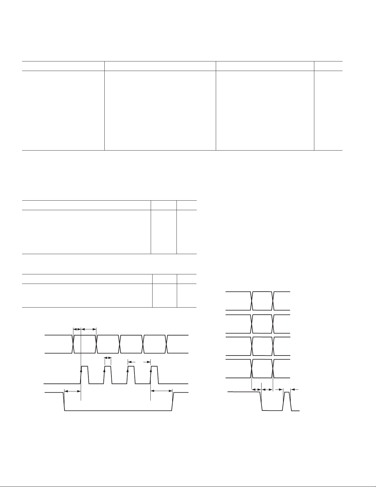
TIMING SPECIFICATIONS
SERIAL PROGRAMMING TIMING REQUIREMENTS
(VS = 5 V, T = 25∞C)
Parameter Typ Unit
Minimum Clock Pulsewidth (T
Minimum Clock Period (T
Minimum Setup Time Data vs. Clock (T
Minimum Setup Time Data Enable vs. Clock (T
Minimum Hold Time Clock vs. Data Enable (T
Minimum Hold Time Data vs. Clock (TDH)4ns
)10ns
PW
)20ns
CK
)2ns
DS
)2 ns
ES
)2 ns
EH
PARALLEL PROGRAMMING TIMING REQUIREMENTS
= 5 V, T = 25∞C)
(V
S
Parameter Typ Unit
Minimum Setup Time Data Enable vs. Data (T
Minimum Hold Time Data Enable vs. Data (T
Minimum Data Enable Width (TPW)4ns
T
T
DH
DS
DATA
(BIT 0)
CLOCK
(BIT 1)
DATA
ENABLE
(DEN B)
CLOCK
DISABLED
MSB MSB–1 MSB–2 LSB
T
PW
T
ES
DATA IS LATCHED ON LOW-TO-HIGH TRANSITION OF DENB
CLOCK
ENABLED
)2 ns
ES
)2 ns
EH
T
CK
T
EH
CLOCK
DISABLED
(NOT TO SCALE)
MSB
(BIT3)
MSB–1
(BIT2)
MSB–2
(BIT1)
LSB
(BIT0)
DENB
DATA IS LATCHED ON HIGH-TO-LOW
TRANSITION OF DENB
Serial Programming Timing
T
ESTEH
T
PW
(NOT TO SCALE)
Parallel Programming Timing
REV. 0–4–
AD8369
ABSOLUTE MAXIMUM RATINGS*
Supply Voltage VS, VPOS . . . . . . . . . . . . . . . . . . . . . . . . 5.5 V
PWUP . . . . . . . . . . . . . . . . . . . . . . . . . . . . . . . . . V
BIT0, BIT1, BIT2, BIT3, DENB, SENB . . . . . . V
Input Voltage, V
Input Voltage, V
Input Voltage, V
INHI
INHI
INHI
– V
or V
– V
................................
. . . . . . . . . . . . . . . . . . . . . . . . 4 V
INLO
with respect to COMM . . 4.5 V
INLO
with respect to COMM
INLO
COMM – 200 mV
+ 200 mV
S
+ 200 mV
S
Internal Power Dissipation . . . . . . . . . . . . . . . . . . . . . 265 mW
. . . . . . . . . . . . . . . . . . . . . . . . . . . . . . . . . . . . . . . 150∞C/W
JA
Maximum Junction Temperature . . . . . . . . . . . . . . . . . 125∞C
Operating Temperature Range . . . . . . . . . . . .–40∞C to +85∞C
Storage Temperature Range . . . . . . . . . . . . . –65∞C to +150∞C
Lead Temperature Range (soldering 60 sec) . . . . . . . to 300∞C
*Stresses above those listed under Absolute Maximum Ratings may cause perma-
nent damage to the device. This is a stress rating only; functional operation of the
device at these or any other condition s above those indicated in the operational
section of this specification is not implied. Exposure to absolute maximum rating
conditions for extended periods may affect device reliability.
ORDERING GUIDE
Model Temperature Range Package Description Package Option
AD8369ARU –40ºC to +85ºC Tube, 16-Lead TSSOP RU-16
AD8369ARU-REEL7 –40ºC to +85ºC 7" Tape and Reel
AD8369EVAL Evaluation Board
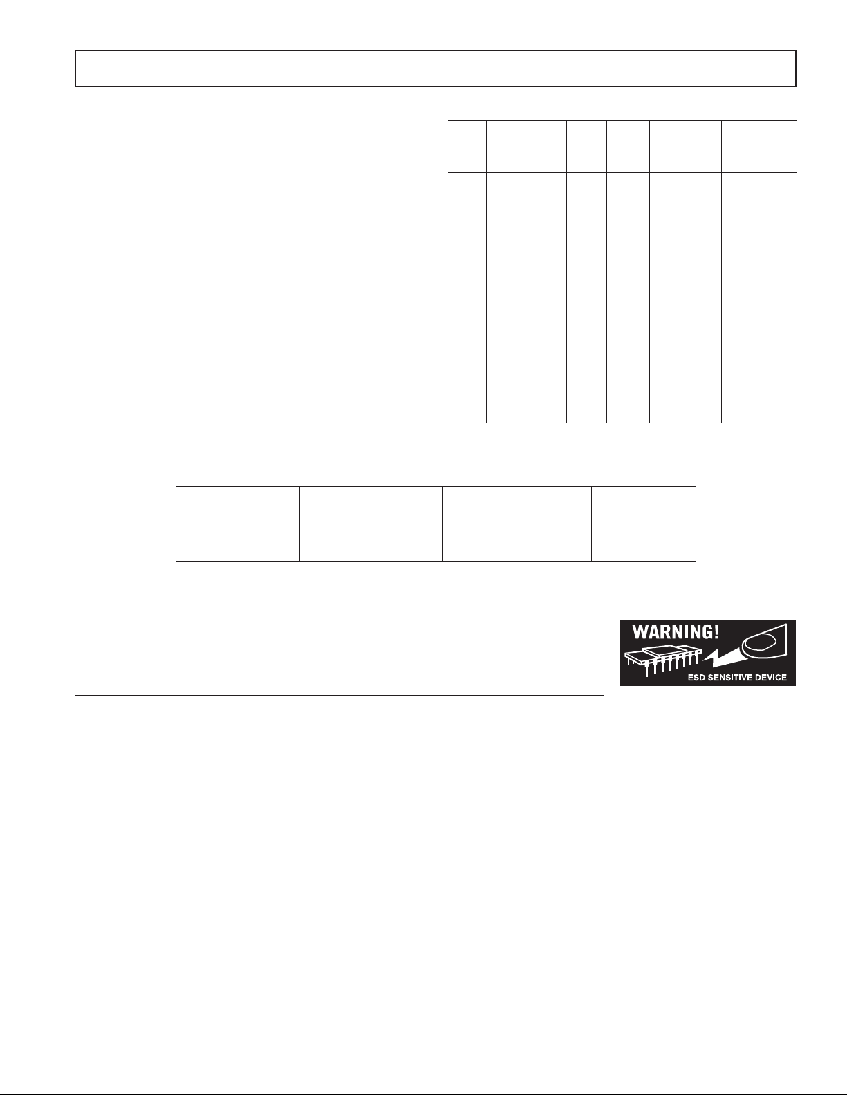
Table I. Typical Voltage Gain vs. Gain Code (VS = 5 V, f = 70 MHz)
Typical Typical
Gain Gain (dB) Gain (dB)
Code BIT3 BIT2 BIT1 BIT0 RL = 1 k⍀ RL = 200 ⍀
00000–5 –10
10001–2 –7
200101 –4
300114 –1
401007 2
5010110 5
6011013 8
7011116 11
8100019 14
9100122 17
10 1 01025 20
11 1 01128 23
12 1 10031 26
13 1 10134 29
14 1 11037 32
15 1 11140 35
CAUTION
ESD (electrostatic discharge) sensitive device. Electrostatic charges as high as 4000 V readily
accumulate on the human body and test equipment and can discharge without detection. Although the
AD8369 features proprietary ESD protection circuitry, permanent damage may occur on devices
subjected to high energy electrostatic discharges. Therefore, proper ESD precautions are recommended
to avoid performance degradation or loss of functionality.
REV. 0
–5–

AD8369
PIN CONFIGURATION
16
INLO
1
2
COMM
AD8369
3
BIT0
BIT1
BIT2
BIT3
DENB
OPLO OPHI
4
5
6
7
8
TOP VIEW
(Not To Scale)
PIN FUNCTION DESCRIPTIONS
Pin No. Mnemonic Function
1 INLO Balanced Differential Input. Internally biased, should be ac-coupled.
2 COMM Device Common. Connect to low impedance ground.
3 BIT0 Gain Selection Least Significant Bit. Used as DATA input signal when in serial mode of operation.
4 BIT1 Gain Selection Control Bit. Used as CLOCK input pin when in serial mode of operation.
5 BIT2 Gain Selection Control Bit. Inactive when in serial mode of operation.
6 BIT3 Gain Selection Most Significant Bit. Inactive when in serial mode of operation.
7 DENB Data Enable Pin. Writes data to register. See Timing Specifications for details.
8 OPLO Balanced Differential Output. Biased to midsupply, should be ac-coupled.
9 OPHI Balanced Differential Output. Biased to midsupply, should be ac-coupled.
10 CMDC Common-Mode Decoupling Pin. Connect bypass capacitor to ground for additional common-mode supply
decoupling beyond the existing internal decoupling.
11 FILT High-Pass Filter Connection. Used to set high-pass corner frequency.
12 SENB Serial or Parallel Interface Select. Connect SENB to VPOS for serial operation. Connect SENB to COMM
for parallel operation.
13 VPOS Positive Supply Voltage, V
= +3 V to +5.5 V.
S
14 PWUP Power-Up Pin. Connect PWUP to VPOS to power up the device. Connect PWUP to COMM to power-down.
15 COMM Device Common. Connect to a low impedance ground.
16 INHI Balanced Differential Input. Internally biased, should be ac-coupled.
INHI
15
COMM
14
PWUP
13
VPOS
12
SENB
11
FILT
10
CMDC
9
REV. 0–6–
Typical Performance Characteristics–AD8369
FREQUENCY – MHz
10
OUTPUT IP3 – dBm
100 1000
35
30
25
20
10
0
15
5
OUTPUT IP3 – dBV rms
28
23
18
13
3
–7
8
–2
(VS = 5 V, T = 25ⴗC, RS = 200 ⍀, Maximum gain, unless otherwise noted.)
50
40
30
20
10
GAIN – dB
0
ⴚ10
ⴚ20
01
23456 78 910
RL = 1k⍀
GAIN CODE
TPC 1. Gain vs. Gain Code at 70 MHz
43
41
39
37
35
33
GAIN – dB
31
29
27
25
10
VS = 3V, RL = 1k⍀
VS = 3V, RL = 200⍀
FREQUENCY – MHz
VS = 5V, RL = 1k⍀
VS = 5V, RL = 200⍀
100 1000
RL = 200⍀
11 12 13 14 15
50
40
30
20
10
GAIN – dB
0
ⴚ10
ⴚ20
10
FREQUENCY – MHz
GAIN CODE 15
GAIN CODE 0
100 1000
TPC 4. Gain vs. Frequency by Gain Code, RL = 1 k
50
40
30
20
10
GAIN – dB
0
ⴚ10
ⴚ20
10
FREQUENCY – MHz
GAIN CODE 15
GAIN CODE 0
100 1000
W
TPC 2. Maximum Gain vs. Frequency by RL and
Supply Voltage
28
26
24
22
OUTPUT IP3 – dBm
18
16
14
23456 78 9102011 12 13 14 15
01
GAIN CODE
TPC 3. Output IP3 vs. Gain Code at 70 MHz, VS = 5 V,
= 200
R
L
W
REV. 0 –7–
21
19
17
15
13
11
OUTPUT IP3 – dBV rms
9
7
TPC 5. Gain vs. Frequency by Gain Code, RL = 200
TPC 6. Output IP3 vs. Frequency, VS = 5 V, RL = 200
Maximum Gain
W
W
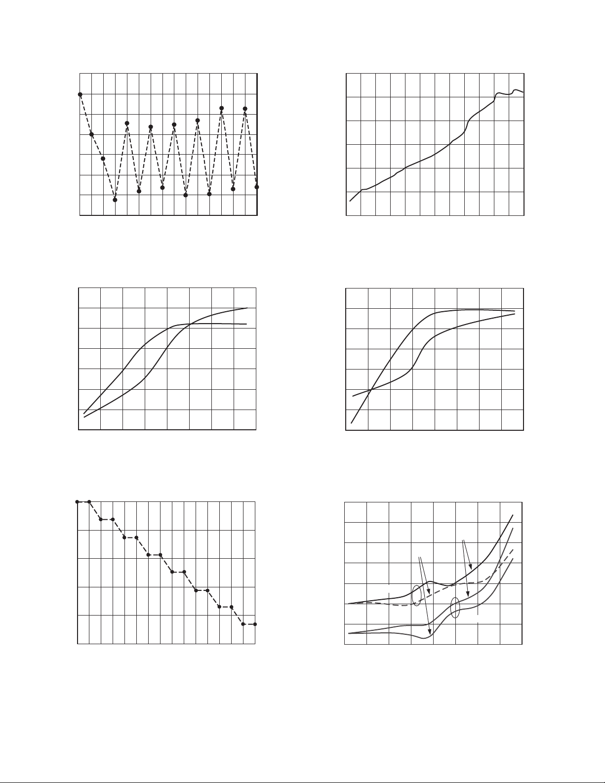
AD8369
–63
–64
–65
–66
–67
OUTPUT IMD – dBc
–68
–69
–70
4
0
3215678
GAIN CODE
91011121314 15
TPC 7. Two-Tone, IMD3 vs. Gain Code at 70 MHz,
V
OPHI
ⴚ40
ⴚ45
ⴚ50
ⴚ55
ⴚ60
– V
= 1 V p-p, VS = 5 V, RL = 1 k
OPLO
HD
3
HD
2
W
–20
–30
–40
–50
–60
OUTPUT IMD – dBc
–70
–80
0
200
15010050 250 300 350 400
FREQUENCY – MHz
TPC 10. Two-Tone IMD3 vs. Frequency V
VS = 5 V, RL = 1 kW, Maximum Gain
ⴚ35
ⴚ40
ⴚ45
ⴚ50
ⴚ55
HD
3
HD
2
450 500 550 600
– V
OPHI
OPLO
= 1 V p-p,
ⴚ65
HARMONIC DISTORTION – dBc
ⴚ70
ⴚ75
050
TPC 8. Harmonic Distortion at V
Frequency, V
50
40
30
20
NOISE FIGURE – dB
10
0
01
100 150 200 250 300 350 400
FREQUENCY – MHz
– V
= 5 V, RL = 1 kW, Maximum Gain
S
23456 78 910
OPHI
GAIN CODE
OPLO
11 12 13 14 15
= 1 V p-p vs.
TPC 9. Noise Figure vs. Gain Code at 70 MHz, VS = 5 V,
= 200
R
L
W
ⴚ60
HARMONIC DISTORTION – dBc
ⴚ65
ⴚ70
050
TPC 11. Harmonic Distortion at V
Frequency, V
8.0
7.8
7.6
7.4
7.2
NOISE FIGURE – dB
7.0
6.8
6.6
050
100 150 200 250 300 350 400
FREQUENCY – MHz
– V
= 5 V, RL = 200 W, Maximum Gain
S
RL = 1k⍀
100 150 200 250 300 350 400
FREQUENCY – MHz
OPHI
5V
3V
RL = 200⍀
TPC 12. Noise Figure vs. Frequency by RL and
Supply Voltage at Maximum Gain
= 1 V p-p vs.
OPLO
REV. 0–8–
 Loading...