

Page 1
800 MHz, Linear-in-dB
V
V
V
V
V
V
P
V
FEATURES
Analog variable gain range: −12 db to +22 dB
Linear-in-dB scaling: 37.5 dB/V
3 dB bandwidth: 800 MHz @ V
Integrated rms detector
P1 dB: 16 dBm @ 140 MHz
Output IP3: 33 dBm @ 140 MHz
Noise figure at maximum gain: 9.5 dB @ 140 MHz
Input and output impedances: 50 Ω
Single-supply voltages from 4.5 V to 5.5 V
RoHS-compliant, 24-lead LFCSP
APPLICATIONS
Complete IF AGC amplifiers
Gain trimming and leveling
Cellular base station
Point-to-point radio links
RF instrumentation
GAIN
= 0.5 V
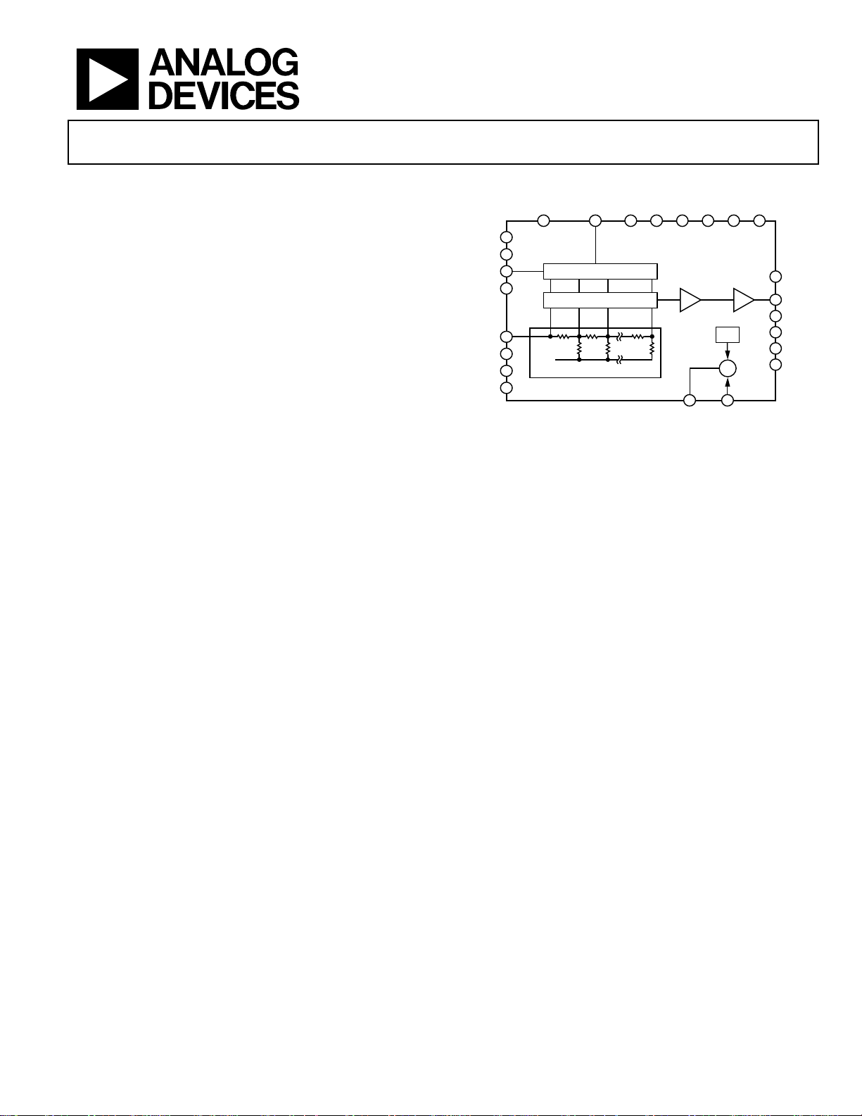
VGA with AGC Detector
AD8368
FUNCTIONAL BLOCK DIAGRAM
PSO
PSI
PSI
PSI
PSI
23
OUTPUT
BUFFER
REF
2
X
PSI
13
24
ENBL
8
OUT
3
HPFL
4
DECL
14
–
+
DECL
15
DECL
05907-001
ICOM
OCOM
GAIN
OCOM
INPT
ICOM
ICOM
ICOM
PSO
10
16
6
1
7
19
17
DECL
18
20
MODE
GAIN INTERPOLATOR
gmSTAGES
0dB –2dB –4d B –36dB
50Ω
ATTENUATO R LADDER
9
21
11
12
AD8368
FIXED-GAIN
AMPLIFIER
2
DETO5DETI
22
Figure 1.
GENERAL DESCRIPTION
The AD8368 is a variable gain amplifier with analog linearin-dB gain control that can be used from low frequencies to
800 MHz. Its excellent gain range, conformance, and flatness
are attributed to Analog Devices’ X-AMP® architecture, an
innovative technique for implementing high performance
variable gain control.
The gain range of −12 dB to +22 dB is scaled accurately to
37.5 dB/V with excellent conformance error. The AD8368 has
a 3 dB bandwidth of 800 MHz that is nominally independent
of gain setting. At 140 MHz, the OIP3 is 33 dBm at maximum gain. The output noise floor is –143 dBm/Hz, which
corresponds to a 9.5 dB noise figure at maximum gain. The
single-ended input and output impedances are nominally 50 Ω.
The gain of the AD8368 can be configured to be an increasing
or decreasing function of the gain control voltage depending on
whether the MODE pin is pulled to the positive supply or to
ground, respectively. When MODE is pulled high, the AD8368
operates as a typical VGA with increasing gain. By connecting
MODE to ground and using the on-board rms detector, the
AD8368 can be configured as a complete AGC system with
RSSI. The output power is accurately leveled to the internal
default setpoint of 63 mV rms (−11 dBm referenced to 50 Ω),
independent of the waveform crest factor. Because the
uncommitted detector input is available at DETI, the AGC loop
can level the signal at the AD8368 output or at any other point
in the signal chain over a maximum input power range of
34 dB. Furthermore, the setpoint level can be raised by dividing
down the output signal before applying it to the detector.
The AD8368 operates from a supply voltage of 4.5 V to 5.5 V
and consumes 60 mA of current. It can be fully powered down
to <3 mA by grounding the ENBL pin. The AD8368 is
fabricated using Analog Devices’ proprietary SiGe SOI
complementary bipolar IC process. It is available in a 24-lead
CSP and operates over the industrial temperature range of
−40°C to +85°C. Application boards are available upon request.
Rev. 0
Information furnished by Analog Devices is believed to be accurate and reliable. However, no
responsibility is assumed by Anal og Devices for its use, nor for any infringements of patents or ot her
rights of third parties that may result from its use. Specifications subject to change without notice. No
license is granted by implication or otherwise under any patent or patent rights of Analog Devices.
Trademarks and registered trademarks are the property of their respective owners.
One Technology Way, P.O. Box 9106, Norwood, MA 02062-9106, U.S.A.
Tel: 781.329.4700 www.analog.com
Fax: 781.461.3113 ©2006 Analog Devices, Inc. All rights reserved.
Page 2

AD8368
TABLE OF CONTENTS
Features .............................................................................................. 1
Fixed-Gain Stage and Output Buffer....................................... 12
Applications....................................................................................... 1
Functional Block Diagram .............................................................. 1
General Description......................................................................... 1
Revision History ............................................................................... 2
Specifications..................................................................................... 3
Absolute Maximum Ratings............................................................ 5
ESD Caution.................................................................................. 5
Pin Configuration and Function Descriptions............................. 6
Typical Performance Characteristics ............................................. 7
Circuit Description......................................................................... 12
Input Attenuator and Interpolator ........................................... 12
REVISION HISTORY
4/06—Revision 0: Initial Version
Output Offset Correction.......................................................... 12
Input and Output Impedances ................................................. 12
Gain Control Interface............................................................... 13
Applications..................................................................................... 14
VGA Operation .......................................................................... 14
AGC Operation .......................................................................... 14
Evaluation Board ............................................................................ 17
Outline Dimensions ....................................................................... 18
Ordering Guide .......................................................................... 18
Rev. 0 | Page 2 of 20
Page 3
AD8368
SPECIFICATIONS
VS = 5 V, T = 25°C, system impedance Z0 = 50 Ω, V
Table 1.
Parameter Min Typ Max Unit Conditions
OVERALL FUNCTION
Frequency Range LF 800 MHz 3 dB bandwidth
Maximum Input 3 V p To avoid input overload
Maximum Output1 2 V p To avoid clipping
AC Input Impedance 50 Ω From INPT to ICOM
AC Output Impedance 50 Ω From OUTP to OCOM
GAIN CONTROL INTERFACE (GAIN)
Gain Span 34 dB
Gain Scaling 37.5 dB/V
−38 dB/V
Gain Accuracy
±0.4
Maximum Gain 22 dB V
Minimum Gain −12 dB V
V
Range 0 1 V
GAIN
Gain Step Response 100 ns For 6 dB gain step
GAIN Input Impedance 10 kΩ From GAIN to ICOM
GAIN Input Bias Current −2 μA
f = 70 MHz
Noise Figure 9.5 dB Maximum gain
Output IP3 34 dBm f1 = 70 MHz, f2 = 71 MHz, V
Output P1dB
1
16 dBm V
f = 140 MHz
Noise Figure 9.5 dB Maximum gain
Output IP3 33 dBm f1 = 140 MHz, f2 = 141 MHz, V
Output P1dB1 16 dBm V
f = 240 MHz
Noise Figure 9.7 dB Maximum gain
Output IP3 33 dBm f1 = 240 MHz, f2 = 241 MHz, V
Output P1dB
1
15 dBm V
f = 380 MHz
Noise Figure 10 dB Maximum gain
Output IP3 29 dBm f1 = 380 MHz, f2 = 381 MHz, V
Output P1dB1 13 dBm V
1
Operation at compression is not recommended due to adverse distortion components.
= 5 V, RF input = 140 MHz, unless otherwise noted.
MODE
dB
= 5 V, 50 mV ≤ V
V
MODE
= 0 V, 50 mV ≤ V
V
MODE
100 mV ≤ V
= 1 V
GAIN
= 0 V
GAIN
= 0 V, V
GAIN
= 0 V, V
GAIN
= 0 V, V
GAIN
= 0 V, V
GAIN
≤ 900 mV
GAIN
= 0 V
MODE
= 0 V
MODE
= 0 V
MODE
= 0 V
MODE
≤ 950 mV
GAIN
≤ 950 mV
GAIN
GAIN
GAIN
GAIN
GAIN
= 1 V, 0 dBm per output tone
= 1 V, 0 dBm per output tone
= 1 V, 0 dBm per output tone
= 1 V, 0 dBm per output tone
Rev. 0 | Page 3 of 20
Page 4
AD8368
VS = 5 V, T = 25°C, system impedance Z0 = 50 Ω, V
Table 2.
Parameter Min Typ Max Unit Conditions
SQUARE LAW DETECTOR (DETI, DETO)
Output Setpoint −11 dBm OUTP connected to DETI
DETI DC Bias Level to ICOM VS/2 V
DETI Impedance 710 Ω
0.6 pF
DETO Output Range
1
0.1 VS/2 V
AGC Step Response 30 μs For −6 dB input power step (C
MODE CONTROL INTERFACE (MODE)
Mode Threshold 3.5 V
MODE Input Bias Current 50 μA
POWER INTERFACE (VPSI, VPSO)
Supply Voltage 4.5 5 5.5 V
Total Supply Current 60 mA ENBL HIGH
Disable Current 2 mA ENBL LOW
ENABLE INTERFACE (ENBL)
Enable Threshold 2.5 V
Enable Response Time 1.5 μs
3 μs
ENBL Input Bias Current 150 μA V
1
Refer to AGC operation in the Applications section.
= 5 V, RF input = 140 MHz, unless otherwise noted.
MODE
Time delay following off to on transition until
output reaches 90% of final value.
Time delay following on to off transition until
supply current is less than 5 mA.
= 5 V
ENBL
DETO
= 1 nF)
Rev. 0 | Page 4 of 20
Page 5
AD8368
ABSOLUTE MAXIMUM RATINGS
Table 3.
Parameter Rating
Supply Voltage, VPSO, VPSI 5.5 V
ENBL and MODE Select Voltage 5.5 V
RF Input Level 20 dBm
Internal Power Dissipation 440 mW
θJA 52°C/W
Maximum Junction Temperature 125°C
Operating Temperature Range −40°C to +85°C
Storage Temperature Range −65°C to +150°C
Lead Temperature (Soldering 60 sec) 300°C
ESD CAUTION
ESD (electrostatic discharge) sensitive device. Electrostatic charges as high as 4000 V readily accumulate on
the human body and test equipment and can discharge without detection. Although this product features
proprietary ESD protection circuitry, permanent damage may occur on devices subjected to high energy
electrostatic discharges. Therefore, proper ESD precautions are recommended to avoid performance
degradation or loss of functionality.
Stresses above those listed under Absolute Maximum Ratings
may cause permanent damage to the device. This is a stress
rating only; functional operation of the device at these or any
other conditions above those indicated in the operational
section of this specification is not implied. Exposure to absolute
maximum rating conditions for extended periods may affect
device reliability.
Rev. 0 | Page 5 of 20
Page 6
AD8368
PIN CONFIGURATION AND FUNCTION DESCRIPTIONS
GAIN
DETO
HPFL
DECL
DETI
OCOM
ENBL23VPSI22VPSI21MODE20ICOM
24
1
2
3
4
5
6
AD8368
TOP VIEW
(Not to Scale)
7 8 9 101112
OUTP
VPSO
OCOM
INPT
19
18
ICOM
17
ICOM
16
ICOM
15
DECL
14
DECL
13
VPSI
VPSI
VPSI
VPSO
05907-002
Figure 2. AD8368 24-Lead LFCSP Pin Out
Table 4. Pin Function Descriptions
Pin No. Name Function
1 GAIN Gain Control.
2 DETO Detector Output. Provides an output error current for the AGC function.
3 HPFL
High-Pass Filter Connection. A capacitor to ground sets the corner frequency of the internal output offset
control loop which controls the minimum usable input frequency.
4, 14, 15 DECL
Decoupling Pin. Nominally ~V
Applications section).
the
/2. Decoupling capacitance may need to be adjusted for AGC operation (see
S
5 DETI Detector Input. DC level referenced to DECL pin.
6, 7 OCOM Connect OCOM to low impedance ground.
16, 17, 18, 20 ICOM Connect ICOM to low impedance ground.
8 OUTP Signal Output. Must be ac-coupled.
9, 10 VPSO
Positive Supply Voltage, 4.5 V to 5.5 V. VPSO and VPSI must be connected together externally and properly
bypassed.
11, 12, 13,
22, 23
VPSI
Positive Supply Voltage, 4.5 V to 5.5 V. VPSO and VPSI must be connected together externally and properly
bypassed.
19 INPT Signal Input. Must be ac-coupled.
21 MODE Gain Direction Control. HIGH for positive slope. LOW for negative slope.
24 ENBL
Apply a positive voltage (2.5V ≤ V
≤ VPSI ) to activate device.
ENBL
Rev. 0 | Page 6 of 20
Page 7

AD8368
TYPICAL PERFORMANCE CHARACTERISTICS
V = 5 V, T = 25°C, system impedance Z
S 0
25
20
15
10
5
0
S21 (dB)
–5
–10
–15
–20
10 100 1000
FREQUENCY (MHz)
Figure 3. Frequency Response vs. V
25
20
= 50 Ω, MODE = 5 V, unless otherwise noted.
1V
0.75V
0.5V
0.25V
0V
05907-003
GAIN
4
70MHz
3
25
20
15
10
5
GAIN (dB)
0
–5
–10
–15
0 0.2 0.4 0. 6 0. 8 1.0
Figure 6. Gain and Conformance Error vs. V
25
20
+85°C
V
GAIN
+25°C
(V)
GAIN
240MHz
–40°C
(f = 240 MHz)
380MHz
4
3
2
1
0
–1
–2
CONFORMANCE ERRO R (dB)
–3
05907-006
–4
4
3
15
10
5
GAIN (dB)
0
–5
–10
–15
0 0.2 0.4 0. 6 0. 8 1.0
Figure 4. Gain and Conformance Error vs. V
25
20
15
10
5
GAIN (dB)
0
–5
–10
–15
0 0.2 0.4 0. 6 0. 8 1.0
Figure 5. Gain and Conformance Error vs. V
+85°C
V
GAIN
+85°C
V
GAIN
+25°C
(V)
GAIN
+25°C
(V)
GAIN
–40°C
(f = 70 MHz)
140MHz
–40°C
(f = 140 MHz)
2
1
0
–1
–2
CONFORMANCE ERRO R (dB)
–3
05907-004
–4
4
3
2
1
0
–1
–2
CONFORMANCE ERRO R (dB)
–3
05907-005
–4
15
10
5
GAIN (dB)
0
–5
–10
–15
0 0.2 0.4 0. 6 0.8 1.0
Figure 7. Gain and Conformance Error vs. V
0.7
0.6
0.5
0.4
0.3
0.2
0.1
0
AMPLITUDE (V)
–0.1
–0.2
–0.3
–0.4
–0.5 –0.4 –0.3 –0.2 –0.1 0 0.1 0.2 0. 3 0.4 0.5
V
V
GAIN
OUTP
+85°C
V
GAIN
TIME (µs)
+25°C
(V)
GAIN
–40°C
(f = 380 MHz)
2
1
0
–1
–2
CONFORMANCE ERRO R (dB)
–3
05907-007
–4
05907-008
Figure 8. Gain Step Time Domain Response (6 dB Gain Step)
Rev. 0 | Page 7 of 20
Page 8

AD8368
40
380MHz
(V)
(V
140MHz
(V)
MODE
+85°C
+25°C
140MHz
= 0 V)
GAIN
MODE
–40°C
MODE
= 0 V)
= 0 V)
70MHz
05907-009
05907-010
05907-011
35
30
25
20
15
10
5
OUTPUT THIRD-ORDER INTERCEPT (dBm)
0
70 110 150 190 230 270 310 350 380
RF INPUT (MHz )
Figure 9. OIP3 vs. Frequency at Maximum Gain (V Figure 12. Output Compression Point vs. Frequency at Maximum Gain
40
35
30
25
20
15
10
5
OUTPUT THIRD-ORDER INTERCEPT (dBm)
0
0 0.2 0.4 0.6 0.8 1.0
0
–10
–20
–30
–40
–50
THIRD-ORDER IMD (dBc)
–60
–70
–80
0 0.2 0.4 0.6 0.8 1.0
70MHz
240MHz
V
Figure 10. OIP3 vs. V
240MHz
V
GAIN
GAIN
380MHz
GAIN
Figure 11. Third-Order IMD vs. V
(Output Power Is 0 dBm per Tone, V
20
18
16
14
12
10
8
6
4
OUTPUT 1d B COMPRESSI ON (dBm)
2
0
70 110 150 190 230 270 310 350 380
20
70MHz
18
16
14
12
240MHz
10
8
6
4
OUTPUT 1d B COMPRESSI ON (dBm)
2
0
0 0.2 0.4 0.6 0. 8 1.0
RF INPUT (MHz)
= 0 V)
(V
MODE
380MHz
V
GAIN
Figure 13. Output Compression Point vs. V
OUTPUT 1d B COMPRESSI ON (dBm)
20
18
16
14
12
10
8
6
4
2
0
70 350 380310270230190150110
5.5V
5.0V
4.5V
RF INPUT (MHz)
+85°C
–40°C
140MHz
(V)
GAIN
Figure 14. Output Compression Point vs. Supply Voltage at Maximum Gain
= 0 V)
(V
MODE
(V
+25°C
MODE
05907-012
05907-013
= 0 V)
05907-014
Rev. 0 | Page 8 of 20
Page 9

AD8368
50
45
40
35
= 0.75V
= 0.5V
V
GAIN
V
GAIN
= 1V
05907-018
30
25
20
NOISE FI GURE (dB)
15
10
5
0
10 100 1000
FREQUENCY (MHz)
Figure 15. Noise Figure vs. Frequency at Maximum Gain (V
MODE
= 0 V)
= 0V
V
GAIN
V
= 0.25V
GAIN
V
GAIN
05907-015
Figure 18. Input Reflection Coefficient vs. Frequency
50
45
40
34
30
25
20
NOISE FI GURE (dB)
15
10
5
0
01
Figure 16. Noise Figure vs. V
0
–5
–10
–15
–20
–25
70MHz
140MHz
240MHz
380MHz
V
GAIN
V
GAIN
(V)
= 1V
GAIN
V
GAIN
(V
= 0.75V
MODE
0.80.60.40.2
= 0 V)
V
GAIN
05907-016
.0
= 0.5V
0
–5
–10
–15
–20
–25
–30
OUTPUT RET URN LOSS (d B)
–35
–40
10 100 1000
Figure 19. Output Reflection Coefficient vs. Frequency
V
GAIN
FREQUENCY (MHz)
= 1V
V
V
GAIN
GAIN
= 1V
= 0V
05907-019
–30
INPUT RETURN LOSS (dB)
–35
–40
10 100 1000
FREQUENCY (MHz)
V
GAIN
= 0.25V
Figure 17. Input Return Loss vs. Frequency
V
GAIN
= 0V
05907-017
Rev. 0 | Page 9 of 20
= 0V
V
GAIN
Figure 20. Output Reflection Coefficient vs. Frequency
05907-020
Page 10

AD8368
1.0
0.9
0.8
0.7
0.6
0.5
RSSI (V)
0.4
0.3
+25°C
0.2
0.1
0
–40 –35 –30 –25 –20 –15 –10 –5 0 5
Figure 21. RSSI (V Figure 24. RSSI (V
1.0
0.9
0.8
0.7
0.6
0.5
RSSI (V)
0.4
0.3
–40°C
0.2
0.1
+25°C
0
–40 –35 –30 –25 –20 –15 –10 –5 0 5
Figure 22. RSSI (V
1.0
0.9
0.8
0.7
0.6
0.5
RSSI (V)
0.4
0.3
–40°C
0.2
0.1
+25°C
0
–40 –35 –30 –25 –20 –15 –10 –5 0 5
+85°C
–40°C
RF INPUT (dBm)
) and Conformance Error vs. Input Power (f = 70 MHz)
DETO
+85°C
RF INPUT (d Bm)
) and Conformance Error vs. Input Power (f = 140 MHz)
DETO
+85°C
RF INPUT (dBm)
+85°C
+85°C
+85°C
+25°C
+25°C
–40°C
+25°C
–40°C
–40°C
1.0
0.8
0.6
0.4
0.2
0
–0.2
–0.4
CONFORMANCE ERRO R (dB)
–0.6
–0.8
05907-021
–1.0
1.0
0.8
0.6
0.4
0.2
0
–0.2
–0.4
CONFORMANCE ERRO R (dB)
–0.6
–0.8
05907-022
–1.0
1.0
0.8
0.6
0.4
0.2
0
–0.2
–0.4
CONFORMANCE ERRO R (dB)
–0.6
–0.8
05907-023
–1.0
1.0
0.9
0.8
0.7
0.6
0.5
RSSI (V)
0.4
0.3
–40°C
0.2
0.1
0
–40 –35 –30 –25 –20 –15 –10 –5 0 5
AMPLITUDE ( V)
CH2 50mV Ω CH3 100mV Ω M20µ s 500MS/s
Figure 25. AGC Time Domain Response (3 dB Power Step, C
80
70
60
50
40
30
SUPPLY CURRENT (mA)
20
10
0
–40 –20 0 20 6040 80
+85°C
+25°C
+25°C
+85°C
RF INPUT (dBm)
) and Conformance Error vs. Input Power (f = 380 MHz)
DETO
V
RSSI
V
OUTP
A CH1 410mV
5.5V
5.0V
4.5V
4.5V
5.0V
2.0ns/PT
5.5V
TEMPERATURE (° C)
–40°C
DETO
1.0
0.8
0.6
0.4
0.2
0
–0.2
–0.4
–0.6
–0.8
–1.0
05907-025
=1 nF)
8
7
6
5
4
3
2
1
0
CONFORMANCE ERRO R (dB)
05907-024
DISABLE CURRENT (mA)
05907-026
Figure 23. RSSI (V
) and Conformance Error vs. Input Power (f = 240 MHz)
DETO
Figure 26. Supply Current and Disable Current vs. Supply Voltage
Rev. 0 | Page 10 of 20
Page 11

AD8368
V
V
ENBL
OUTP
50
40
30
AMPLITUDE ( V)
CH2 500mV Ω CH3 5V Ω M2.0µs 250MS/s
4.0ns/PT
A CH3 0.0V
Figure 27. ENBL Response Time
50
40
30
20
PERCENTAGE (%)
10
0
36.8 37.0 37.2 37.4 37.6 37.8 38.0 38.2
SLOPE (dB/V)
Figure 28. Gain Scaling Distribution (140 MHz)
20
PERCENTAGE (%)
10
05907-027
0
–15.0 –13.5–13.8–14.1–14.4–14.7
INTERCEPT ( dB)
05907-029
Figure 29. Gain Intercept Distribution (140 MHz)
05907-028
Rev. 0 | Page 11 of 20
Page 12

AD8368
VOUT
CIRCUIT DESCRIPTION
The AD8368 is a single-ended VGA with a bandwidth of
800 MHz and a gain control span of 34 dB ranging from −12 dB
to +22 dB. It incorporates an uncommitted square law detector
that can be used to form a tight AGC loop around the VGA.
Using Analog Devices’ patented X-AMP architecture, the
AD8368 achieves accurate linear-in-dB gain control with
excellent linearity (OIP3) and noise figure (NF). The part also
features 50 Ω input and output impedances for ease of use.
The main signal path, shown in
input attenuator followed by a fixed-gain amplifier and output
stage. This architecture allows for a constant OIP3 and output
noise floor as a function of gain setting. As a result, NF and IIP3
increase 1 dB for every 1 dB decrease in gain, resulting in a part
with constant dynamic range over gain setting.
MODE
GAIN
INPT
GAIN INTERPO LATOR
gmSTAGES
0dB –2dB –4dB – 36dB
50Ω
DECL
ATTENUATOR LADDER
Figure 30. Simplified Block Diagram
INPUT ATTENUATOR AND INTERPOLATOR
The input attenuator is built from an 18-section resistor ladder
providing 2 dB of attenuation at each successive tap point. The
resistor ladder acts as a linear input attenuator, in addition to
providing an accurate 50 Ω input impedance. The variable
transconductance (g
) stages are used to select the attenuated
m
signal from the appropriate tap point along the ladder and feed
this signal to the fixed-gain amplifier. To realize a continuous gain
control function from discrete tap points, the gain interpolator
creates a weighted sum of signals appearing on adjacent tap
points by carefully controlling the variable g
FIXED-GAIN STAGE AND OUTPUT BUFFER
The weighted sum of the different tap points is fed into the
fixed-gain stage which drives the output buffer. Because the
resistive input attenuator is linear and contributes minimal
noise as a passive termination, the dynamic range as a function
of gain is determined primarily by the noise and distortion of
the fixed-gain amplifier. This explains the constant OIP3 and
constant output noise floor with gain setting and the
corresponding dB-for-dB increase in IIP3 and NF with
decreasing gain. The output buffer has 6 dB of gain and
provides a broadband 50 Ω single-ended output impedance.
Figure 30, consists of a variable
FIXED-GAIN
AMPLI FIER
stages.
m
OUTPUT
BUFFER
05907-033
OUTPUT OFFSET CORRECTION
The dc level at the input, INPT, is driven by an internal
reference to V
pin for external decoupling with C
/2. The reference is made available at the DECL
S
. The dc level at the output,
DECL
OUTP, is regulated to the same midsupply reference by an offset
correction loop independent of gain setting, temperature, and
process. The low-pass response of this loop creates a high-pass
corner frequency in the signal path transfer function, which can
be set by choosing C
FROM
INTERPOL ATOR
g
STAGES
m
Figure 31. Output Centering Control Loop
DECL
and C
FIXED-GAIN
AMPLIFI ER
HPFL
HPFL
C
.
OUTPUT
BUFFER
VOUT
g
m
HP
DECL
C
DECL
×1
V
MID
05907-034
The input and output coupling capacitors should be selected to
provide low impedances at the frequencies of interest relative to
50 Ω so as not to affect the high-pass corner. In this case, the
high-pass corner frequency can be set by either C
HPFL
or C
DECL
which form independent poles in the feedback path of the offset
correction loop. The high-pass corner is determined by the
highest of these poles, which are given by:
8.0
5700
Cf+
Cf+
HPFL
DECL
)005.0(
)005.0(
where C
,
HPFLHP
,
DECLHP
HPFL DECL
)kHz(
=
)kHz(
=
and C are in nF.
When using this method to set the high-pass frequency, the
other capacitor should be sized such that its pole is at least
30× lower in frequency. Also note that C
represents the total
DECL
decoupling capacitance at the DECL pins.
INPUT AND OUTPUT IMPEDANCES
The AD8368 offers single-ended broadband 50 Ω input and
output impedances. The excellent match to 50 Ω is maintained
from part to part, over frequency, and over gain setting. Both
the input and output pins must be externally ac coupled to
prevent disruption of the internal dc levels. Sufficiently large
coupling capacitors should be used so that their impedance is
negligible relative to the 50 Ω presented by the ladder at the
input and by the output buffer at the output.
Rev. 0 | Page 12 of 20
Page 13

AD8368
GAIN CONTROL INTERFACE
The AD8368 has a linear-in-dB gain control interface that can
be operated in either a gain-up mode or gain-down mode. In
the gain-up mode with the MODE pin pulled high, the gain
increases with increasing gain voltages. In the gain-down mode,
with the MODE pin pulled low, the gain decreases with
increasing gain voltages. In both modes of operation, the gain
control slope is maintained at +37.5 dB/V or −38 dB/V
(depending on mode selection) over temperature, supply, and
process as V
MODE LOW is required to form an AGC loop with the onboard detector around the VGA.
The gain functions for MODE pulled high and low are given
respectively by:
HIGH
LOW
where V
varies from 100 mV to 900 mV. Note that
GAIN
145.37)dB( −×= GAIN
VGain
GAIN
VGain
is expressed in volts.
GAIN
8.2438)dB( +×−=
25
20
15
10
GAIN (dB)
–5
–10
–15
5
0
010.80.60.40.2
V
GAIN
(V)
Figure 32. Gain and Conformance Error vs. V
GAIN_H
ERROR_L
ERROR_H
GAIN_L
GAIN
As shown in Figure 32, the gain function can be either an
increasing or decreasing function of V
, depending on the
GAIN
MODE pin.
4
3
2
1
0
–1
–2
CONFORMANCE ERRO R (dB)
–3
05907-035
–4
.0
Rev. 0 | Page 13 of 20
Page 14

AD8368
V
V
APPLICATIONS
VGA OPERATION
The AD8368 is a general-purpose VGA suitable for use in a wide
variety of applications where accurate, continuous, linear-in-dB
gain control over a broad range of frequencies is important. Its
stability over temperature and supply in comparison to other
variable-gain techniques can be traced back to the X-AMP
architecture. While having an 800 MHz bandwidth, its low
frequency operation can be extended by properly selecting C
DECL
.
and C
The typical connections for using the AD8368 in VGA mode
are illustrated in
Figure 33. The input (INPT) and output (OUTP)
of the AD8368 should be externally ac coupled to prevent
disrupting the dc levels on the chip. Thus, a sufficiently large
coupling capacitor should be used such that the series impedance
of the capacitor is negligible at the frequencies of interest.
IN
V
POS
VPSI
V
GAIN
0V TO 1V
VPSI
ENBL
2
REF
X
–
+
AD8368
OCOM
OUTP
VPSO
MODE
VPSO
V
OUT
ICOM
VPSI
INPT
ICOMGAIN
ICOMDETO
ICOMHPFL
DECLDECL
DECLDETI
VPSIOCOM
VPSI
Figure 33. Typical Connections for VGA Mode for Increasing Gain with
Increasing V
(MODE HIGH)
GAIN
The gain control voltage ranging from 0 V to 1 V is applied to
the GAIN pin. The MODE pin controls whether the gain of the
part is an increasing or decreasing function of the gain voltage.
When the MODE pin is pulled high, the gain increases with
increasing gain voltages. When the MODE pin is pulled low, the
gain decreases with increasing gain voltages. The ENBL pin is
used to enable or disable the part. ENBL is active high; when
ENBL is pulled low, the part is disabled and draws a fraction of
the normal supply current.
HPFL
V
POS
05907-036
The DECL pin provides the internal midsupply dc reference
for the AD8368. It should be well decoupled to ground using
a large capacitor with low ESR. The capacitors connected to
the HPFL pin and DECL pin are used to control the low-pass
corner frequency of the output offset correction loop. The
resulting high-pass corner frequency is inversely proportional
to their values.
AGC OPERATION
The AD8368 can be configured as a standalone AGC amplifier
by using the on-board rms detector, as shown in
Figure 34. The
detector output, DETO, is an error current representing the
difference of squares between the root-mean-square (rms) of
the sensed signal and an internal reference of 63 mV rms. This
error current is integrated on C
and connected to the GAIN
DETO
pin to form the AGC loop.
The 63 mV rms reference corresponds to 178 mV p-p for a sine
wave but the detector accuracy is maintained for more complex
signals such as Gaussian noise, complex envelopes, and multicarrier signals with high peak-to-average ratios.
IN
V
POS
VPSI
RSSI
C
DETO
VPSI
ENBL
2
REF
X
R2
R1
–
+
AD8368
OCOM
OUTP
VPSO
INPT
ICOM
MODE
ICOMGAIN
ICOMDE TO
ICOMHP FL
DECLDECL
DECLDET I
VPSIOCOM
VPSO
VPSI
VPSI
V
POS
V
OUT
05907-037
Figure 34. AGC Mode of Operation
The AGC mode of operation requires a specific gain direction.
The gain must fall as V
increases to restore the needed
DETO
balance against the setpoint. Therefore, the MODE pin must
be pulled low. By connecting the signal at OUTP directly to
the detector input (DETI), the output level is driven to the
63 mV rms reference setpoint.
Rev. 0 | Page 14 of 20
Page 15

AD8368
The output setpoint may be increased using an external resistive
divider network between OUTP and DETI, referenced to DECL
as depicted in
Figure 34. In this configuration, the rms output
voltage is forced to (1 + R1/R2)63 mV rms by the AGC loop.
For a 0 dBm (224 mV rms referenced to 50 Ω) output setpoint,
this ratio is 3.5. After correcting for the input impedance of
DETI, the choice of R1 = 226 Ω and R2 = 100 Ω yields a
setpoint of roughly 0 dBm. This very accurate leveling function
is shown in
Figure 35, where the rms output is held to within
0.2 dB of the 0 dBm setpoint for >30 dB range of input levels.
10
Figure 36 shows a plot of the RSSI voltage at DETO as input
power is swept.
3.0
2.5
2.0
1.5
RSSI (V)
1.0
5
0
–5
–10
–15
POWER OUT (dBm)
–20
–25
–30
–40 –30 –20 –10 0 10 20
POWER IN (d Bm)
05907-038
Figure 35. Output Power vs. Input Power in AGC Mode at 140 MHz
Note that to achieve the accurate level of AGC output power,
the DECL capacitor must be adjusted for the corresponding RF
frequency. The DECL capacitor value varies depending on
board parasitics.
Tabl e 5 shows the DECL capacitor value based
on the evaluation board parasitics.
Table 5.
IF Frequency (MHz) C4 (pF) C20 (pF)
70 1000 2200
140 270 560
240 68 150
380 33 68
480 15 39
A valuable feature of using a square law detector in AGC mode
is that the RSSI voltage is a true reflection of signal power and
may be converted to an absolute power measurement for any
given source impedance. The RSSI in units of dBm referenced
to 50 Ω and based on the voltage available on the DETO pin is
given by
RSSI = −11 + 20 log
(1 + R1/R2) + 38 × V − 24.8
10
DETO
0.5
0
–40 –30 –20 –10 0 10 20
POWER IN (d Bm)
05907-039
Figure 36. Monitoring the GAIN/DETO RSSI Voltage vs. Input Power
In some cases, it may be found that, if driven into AGC
overload, the AD8368 requires unusually long times to recover;
that is, the voltage at DETO remains at an abnormally high
value, and the gain is at its lowest value. To avoid this situation,
it is recommended that a clamp be placed on the DETO pin as
shown in
Figure 37.
ICOMGAIN
ICOMDE TO
ICOMHP FL
DECLDECL
INPT
ICOM
MODE
VPSI
V
AGC
Q1
2N2907
VPSI
ENBL
RB
0.5V
RA
C
AGC
0.1µF
+V
S
Figure 37. External Clamp to Prevent AGC Overload
AD8368
VPSIOCOM
DECLDETI
VPSI
VPSI
VPSO
VPSO
OUTP
OCOM
05907-042
The resistive divider network, RA and RB, should be designed
such that the base of Q1 is driven to 0.5 V.
Rev. 0 | Page 15 of 20
Page 16

AD8368
The choice of C
response time, and carrier leakage. If C
small to speed up the response time, the AGC loop could start
tracking and leveling any amplitude envelope and corrupt the
constellation.
constellation with a degraded error vector magnitude (EVM)
of 5%. By increasing C
to 1.1%.
REF –4.9dBm CF 100 MHz
1U
is a compromise of averaging time constant,
DETO
is selected to be too
DETO
Figure 38 illustrates a 16 QAM, 100 ksymbols/s
to 0.01 μF, the EVM is improved
DETO
SR 10kHz
16 QAM
MEAS SIGNAL
CONST DI AG
Figure 39 illustrates the measured EVM performance for a
16 QAM modulation at 10 Msymbols/s using C
10
9
8
7
6
5
EVM (%)
4
3
2
1
0
–40 –30 –20 –10 0 10 20
Figure 39. Error Vector Magnitude Performance for 16 QAM
POWER IN (d Bm)
10 Msymbols/s
DETO
= 1 nF.
05907-041
–1U
–1.31289U 262.578mU/ 1.31289U
05907-040
Figure 38. Degraded Error Vector Magnitude Performance for 16 QAM at
100 ksymbols/s(C
Too Small)
DETO
Rev. 0 | Page 16 of 20
Page 17

AD8368
V
V
V
V
EVALUATION BOARD
POS
POS1 VPOS2 VPOS3
C20
1nF
DECLDECL
R32
OPEN
VPSIOCOM
DECLDET I
VPSI
VPSI
VPSO
VPSO
OUTP
OCOM
OPEN
R31
C1
OPEN
C
10nF
R30
OPEN
OUT
OUTPUT
DET_IN
C11
1nF
C12
1nF
R11
0Ω
R12
0Ω
C14
0.1µF
C15
0.1µF
POS2
POS3
05907-043
10kΩ
C13
0.1µF
ENABLE
R1
INPUT
VPOS1
10kΩ
LOW
OFF
R2
HI
ON
GAIN
C
IN
10nF
SW1
R10
0Ω
SW2
C10
1nF
DET_OUT_TP
GAIN
INPT
ICOM
MODE
VPSI
VPSI
ENBL
R35
OPEN
JP4
1nF
ICOMGAIN
C6
ICOMDETO
ICOMHPFL
AD8368
C23
10nF
C4
1nF
Figure 40.
Table 6. Evaluation Board Configuration Options
Component Function Default Conditions
R1, R2 Pull-Down Resistors for Mode and Enable. R1 = R2 = 10 kΩ
R10, R11, R12,
C10, C11, C12,
C13, C14, C15
C RF Input. C
IN IN
C RF Output. C
OUT IN
R31, R32
Supply Decoupling. Jumpers, power supply decoupling resistors, and filter
capacitors.
provides dc block for RF input. CIN = 10 nF
provides dc block for RF output. C
Feedback Path for AGC Operation. For a default setpoint of 63 mV rms, set R31 = 0 Ω
R10 = R11 = R12 = 0 Ω
C10 = C11 = C12 = 1 nF
C13 = C14 = C15 = 0.1 μF
= 10 nF
OUT
R31 = R32 = open (VGA mode)
and remove R32. For other AGC setpoints, the rms voltage is determined from
(1 + n) × 63 mV rms, where n = R31/R32.
R35 Populate with 0 Ω to feed detector output RSSI voltage to DET_OUT_TP. R35 = open
C23 Sets the corner frequency of output offset control loop high-pass filter. C23 = 10 nF
C1, R30
C6
C20, C4
JP4
Used for driving detector externally. Set R30 to 50 Ω for matching. Set C1 to be a
large ac coupling cap.
DETO Capacitor. Needs to be made larger for lower data rates (see the
Operation
section).
AGC
DECL Capacitor. Needs to be adjusted based on RF frequency in AGC operation
(see the
AGC Operation section).
Jumper for AGC Mode of Operation. Provides feedback from the detector output to
C1 = not populated
R30 = not populated
C6 = 1 nF
C20 = C4 = 1 nF
JP4 = not populated (VGA mode)
the gain pin.
SW1
Mode Switch. LOW mode puts the part in gain down mode. HIGH puts the part in
SW1 = JP2
gain up mode. AGC operation requires gain down mode.
SW2 Power-Down. The part is disabled when the enable pin is tied to ground. SW2 = JP3
Rev. 0 | Page 17 of 20
Page 18

AD8368
OUTLINE DIMENSIONS
4.00
PIN 1
INDICATOR
1.00
0.85
0.80
SEATING
PLANE
12° MAX
BSC SQ
TOP
VIEW
0.80 MAX
0.65 TYP
COMPLIANT TO JEDEC STANDARDS MO-220-VGGD-8
0.30
0.23
0.18
3.75
BSC SQ
0.20 REF
0.60 MAX
0.05 MAX
0.02 NOM
COPLANARITY
0.08
0.50
BSC
0.50
0.40
0.30
Figure 41. 24-Lead Lead Frame Chip Scale Package [LFCSP_VQ]
4 mm × 4 mm Body, Very Thin Quad
(CP-24-4)
Dimensions shown in millimeters
ORDERING GUIDE
Model
AD8368ACPZ-REEL7 −40°C to +85°C 24-Lead Lead Frame Chip Scale Package (LFCSP_VQ) CP-24-4 1500
AD8368ACPZ-WP −40°C to +85°C 24-Lead Lead Frame Chip Scale Package (LFCSP_VQ) CP-24-4 64
AD8368-EVALZ Evaluation Board
1
Z = Pb-free part.
2
WP = Waffle pack.
1
1, 2
1
Temperature
Range
Package Description
0.60 MAX
19
18
EXPOSED
(BOTTOMVIEW)
13
12
PA D
24
6
7
1
2.50 REF
PIN 1
INDICATOR
2.65
2.50 SQ
2.35
0.23 MIN
Package
Option
Ordering
Quantity
Rev. 0 | Page 18 of 20
Page 19

AD8368
NOTES
Rev. 0 | Page 19 of 20
Page 20

AD8368
NOTES
©2006 Analog Devices, Inc. All rights reserved. Trademarks and
registered trademarks are the property of their respective owners.
D05907-0-4/06(0)
Rev. 0 | Page 20 of 20
 Loading...