500 MHz, Linear-in-dB VGA
a
FEATURES
Broad Range Analog Variable Gain
–2.5 dB to +42.5 dB
3 dB Cutoff Frequency of 500 MHz
Gain Up and Gain Down Modes
Linear-in-dB, Scaled 20 mV/dB
Resistive Ground Referenced Input
Nominal Z
On-Chip Square-Law Detector
Single-Supply Operation: 2.7 V to 5.5 V
APPLICATIONS
Cellular Base Station
Broadband Access
Power Amplifier Control Loops
Complete, Linear IF AGC Amplifiers
High-Speed Data I/O
GENERAL DESCRIPTION
The AD8367 is a high-performance 45 dB variable gain amplifier with linear-in-dB gain control for use from low frequencies
up to several hundred megahertz. The range, flatness, and accuracy of the gain response are achieved using Analog Devices’
®
X-AMP
architecture, the most recent in a series of powerful
proprietary concepts for variable gain applications, which far
surpasses what can be achieved using competing techniques.
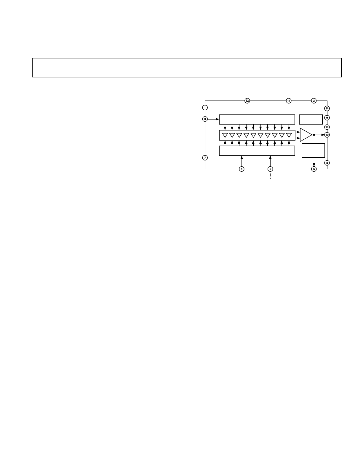
The input is applied to a 200 Ω resistive ladder network, having
nine sections each of 5 dB loss, for a total attenuation of 45 dB.
At maximum gain, the first tap is selected; at progressively lower
gains, the tap moves smoothly and continuously toward higher
attenuation values. The attenuator is followed by a 42.5 dB
fixed gain feedback amplifier—essentially an operational amplifier with a gain bandwidth product of 100 GHz—and is very
linear, even at high frequencies. The output third order intercept is
+20 dBV at 100 MHz (+27 dBm re 200 Ω), measured at an
output level of 1 V p-p with V
ⴝ 200 ⍀
IN
= 5 V.
S
with AGC Detector
AD8367
FUNCTIONAL BLOCK DIAGRAM
VPSOVPSI
ICOM
INPT
ICOM
CELLS
AD8367
9-STAGE ATTENUATOR BY 5dB
g
m
GAUSSIAN INTERPOLATOR
The analog gain-control interface is very simple to use. It is
scaled at 20 mV/dB, and the control voltage, V
50 mV at –2.5 dB to 950 mV at +42.5 dB. In the inverse-gain
mode of operation, selected by a simple pin-strap, the gain
decreases from +42.5 dB at V
V
= 950 mV. This inverse mode is needed in AGC applications,
GAIN
= 50 mV to –2.5 dB at
GAIN
which are supported by the integrated square-law detector,
whose set point is chosen to level the output to 354 mV rms,
regardless of the waveshape. A single external capacitor sets up
the loop averaging time.
The AD8367 may be powered on or off by a voltage applied to
the ENBL pin. When this voltage is at a logic LO, the total power
dissipation drops to the milliwatt range. For a logic HI, the chip
powers-up rapidly to its normal quiescent current of 26 mA at
25°C. The AD8367 is available in a 14-lead TSSOP package for
the industrial temperature range of –40°C to +85°C.
ENBL
BIAS
SQUARE
LAW
DETECTOR
DETOGAINMODE
, runs from
GAIN
ICOM
DECL
HPFL
VOUT
OCOM
X-AMP is a registered trademark of Analog Devices, Inc.
REV. 0
Information furnished by Analog Devices is believed to be accurate and
reliable. However, no responsibility is assumed by Analog Devices for its
use, nor for any infringements of patents or other rights of third parties that
may result from its use. No license is granted by implication or otherwise
under any patent or patent rights of Analog Devices.
One Technology Way, P.O. Box 9106, Norwood, MA 02062-9106, U.S.A.
Tel: 781/329-4700www.analog.com
Fax: 781/326-8703 © Analog Devices, Inc., 2001

AD8367–SPECIFICATIONS
(VS = 5 V, TA = 25ⴗC, System Impedance ZO = 200 ⍀, V
unless otherwise noted.)
= 5 V, f = 10 MHz,
MODE
Parameter Conditions Min Typ Max Unit
OVERALL FUNCTION
Frequency Range LF 500 MHz
GAIN Range 45 dB
INPUT STAGE Pins INPT and ICOM
Maximum Input To Avoid Input Overload 700 mV p-p
Input Resistance From INPT to ICOM 175 200 225 Ω
GAIN CONTROL INTERFACE Pin GAIN
Scaling Factor V
Gain Law Conformance 100 mV ≤ V
Maximum Gain V
Minimum Gain V
V
Step Response From 0 dB to 30 dB 300 ns
GAIN
= 5 V, 50 mV ≤ V
MODE
= 0 V, 50 mV ≤ V
V
MODE
= 0.95 V +42.5 dB
GAIN
= 0.05 V –2.5 dB
GAIN
≤ 900 mV ± 0.2 dB
GAIN
≤ 950 mV +20 mV/dB
GAIN
≤ 950 mV –20 mV/dB
GAIN
From 30 dB to 0 dB 300 ns
Small Signal Bandwidth V
= 0.5 V 5 MHz
GAIN
OUTPUT STAGE Pin VOUT
Max Output Voltage Swing RL = 1 kΩ 4.3 V p-p
R
= 200 Ω 3.5 V p-p
Output Source Resistance Series Resistance of Output Buffer 50 Ω
Output Centering Voltage
1
L
VS/2 V
SQUARE LAW DETECTOR Pin DETO
Output Set Point 354 mV rms
AGC Small Signal Response Time C
100 pF, 6 dB Gain Step 1 s
AGC
POWER INTERFACE Pins VPSI, VPSO, ICOM, and OCOM
Supply Voltage 2.7 5.5 V
Total Supply Current ENBL High, Maximum Gain, R
200 Ω 26 30 mA
L
(Includes Load Current)
Disable Current vs. Temperature ENBL Low 1.3 1.6 mA
–40°C ≤ TA ≤ +85°C 1.8 mA
MODE CONTROL INTERFACE Pin MODE
Mode LO Threshold Device in Negative Slope Mode of Operation 1.2 V
Mode HI Threshold Device in Positive Slope Mode of Operation 1.4 V
ENABLE INTERFACE Pin ENBL
Enable Threshold 2.5 V
Enable Response Time Time Delay Following LO to HI Transition 1.5 s
until Device Meets Full Specifications.
Enable Input Bias Current ENBL at 5 V 27 A
ENBL at 0 V 32 nA
–2–
REV. 0

AD8367
Parameter Conditions Min Typ Max Unit
f = 70 MHz
Gain Maximum Gain +42.5 dB
Minimum Gain –3.7 dB
Gain Scaling Factor 19.9 mV/dB
Gain Intercept –5.6 dB
Noise Figure Maximum Gain 6.2 dB
Output IP3 f1 70 MHz, f2 71 MHz, V
Output 1 dB Compression Point V
0.5 V 8.5 dBm
GAIN
f = 140 MHz
Gain Maximum Gain +43.5 dB
Minimum Gain –3.6 dB
Gain Scaling Factor 19.7 mV/dB
Gain Intercept –5.3 dB
Noise Figure Maximum Gain 7.4 dB
Output IP3 f1 140 MHz, f2 141 MHz, V
Output 1 dB Compression Point V
0.5 V 8.4 dBm
GAIN
f = 190 MHz
Gain Maximum Gain +43.5 dB
Minimum Gain –3.8 dB
Gain Scaling Factor 19.6 mV/dB
Gain Intercept –5.3 dB
Noise Figure Maximum Gain 7.5 dB
Output IP3 f1 190 MHz, f2 191 MHz, V
Output 1 dB Compression Point V
0.5 V 8.4 dBm
GAIN
f = 240 MHz
Gain Maximum Gain +43 dB
Minimum Gain –4.1 dB
Gain Scaling Factor 19.7 mV/dB
Gain Intercept –5.2 dB
Noise Figure Maximum Gain 7.6 dB
Output IP3 f1 240 MHz, f2 241 MHz, V
Output 1 dB Compression Point V
NOTES
1
The output dc centering voltage is normally set at VS2 and can be adjusted by applying a voltage to DECL.
Specifications subject to change without notice.
0.5 V 8.1 dBm
GAIN
0.5 V 27.5 dBm
GAIN
20.5 dBV rms
1.5 dBV rms
0.5 V 24.5 dBm
GAIN
17.5 dBV rms
1.4 dBV rms
0.5 V 23.9 dBm
GAIN
16.9 dBV rms
1.4 dBV rms
0.5 V 24.6 dBm
GAIN
17.6 dBV rms
1.1 dBV rms
REV. 0
–3–

AD8367
WARNING!
ESD SENSITIVE DEVICE
ABSOLUTE MAXIMUM RATINGS*
Supply Voltage VPSO, VPSI . . . . . . . . . . . . . . . . . . . . . 5.5 V
ENBL Voltage . . . . . . . . . . . . . . . . . . . . . . . . . . V
MODE Select Voltage . . . . . . . . . . . . . . . . . . . . V
V
Control Voltage . . . . . . . . . . . . . . . . . . . . . . . . . . 1.2 V
GAIN
+ 200 mV
S
+ 200 mV
S
Input Voltage . . . . . . . . . . . . . . . . . . . . . . . . . . . . . . ± 600 mV
Internal Power Dissipation . . . . . . . . . . . . . . . . . . . . 250 mW
. . . . . . . . . . . . . . . . . . . . . . . . . . . . . . . . . . . . . . 150°C/W
θ
JA
Maximum Junction Temperature . . . . . . . . . . . . . . . . 125°C
Operating Temperature Range . . . . . . . . . . . –40°C to +85°C
Storage Temperature Range . . . . . . . . . . . . –65°C to +150°C
Lead Temperature Range (Soldering 60 sec) . . . . . . . . 300°C
*Stresses above those listed under Absolute Maximum Ratings may cause perma-
nent damage to the device. This is a stress rating only; functional operation of the
device at these or any other conditions above those indicated in the operational
section of this specification is not implied. Exposure to absolute maximum rating
conditions for extended periods may affect device reliability.
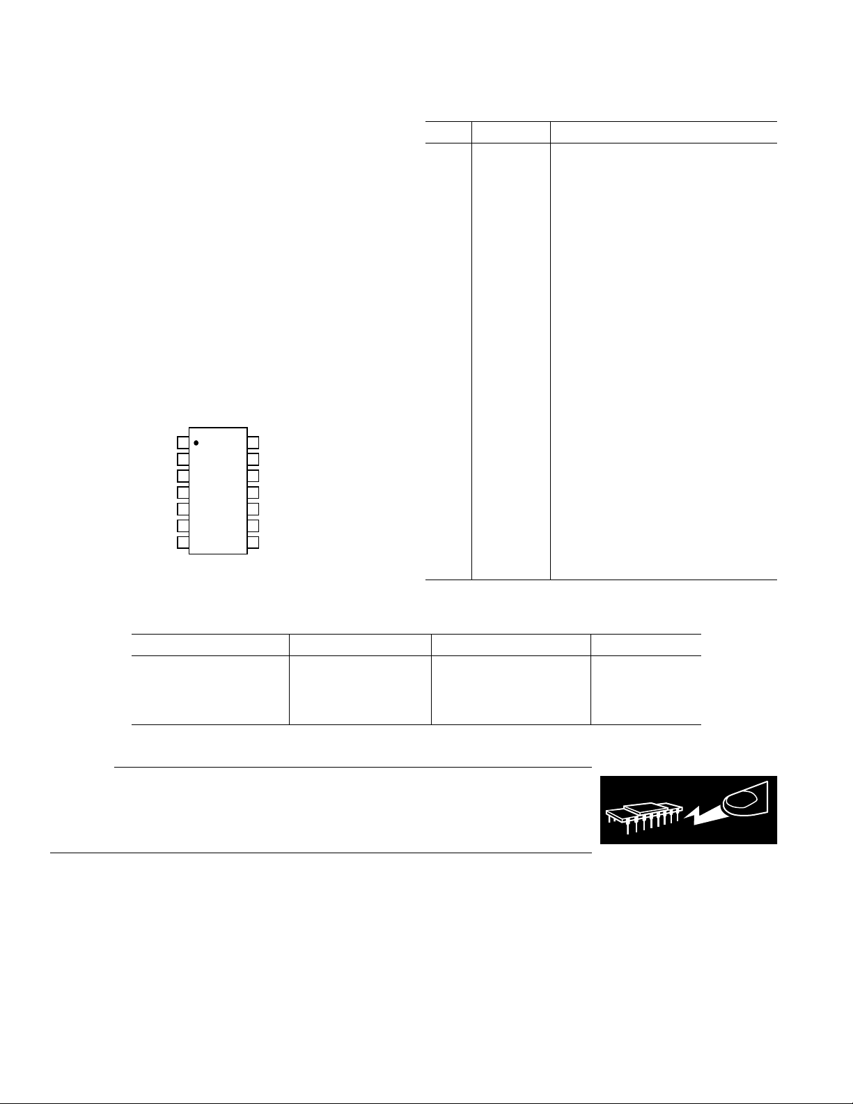
PIN CONFIGURATION
ICOM
ENBL
INPT
MODE
GAIN
DETO
ICOM
1
2
3
AD8367
4
TOP VIEW
(Not to Scale)
5
6
7
14
13
12
11
10
9
8
ICOM
HPFL
VPSI
VPSO
VOUT
DECL
OCOM
PIN FUNCTION DESCRIPTIONS
Pin Mnemonic Description
1, 7, 14 ICOM Signal Common. Connect to low
impedance ground.
2 ENBL A HI activates the device.
3 INPT Signal Input. 200 Ω to ground.
4 MODE Gain Direction Control. HI for Positive
Slope; LO for Negative Slope.
5 GAIN Gain-Control Voltage Input
6 DETO Detector Output. Provides output cur-
rent for RSSI function and AGC control.
8 OCOM Power Common. Connect to low
impedance ground.
9 DECL Decoupling Pin. Can Be Used to
Modify the Output Reference Level.
10 VOUT Signal Output. Generally will be
ac-coupled.
11 VPSO Positive Supply Voltage. 2.7 V to 5.5 V.
VPSI and VPSO are tied together internally with back-to-back PN junctions.
They should be tied together externally
and properly bypassed.
12 VPSI Positive Supply Voltage. 2.7 V to 5.5 V.
13 HPFL High-Pass Filter Connection. A capaci-
tor to ground sets the corner frequency
of the output offset control loop.
ORDERING GUIDE
Model Temperature Range Package Description Package Option
AD8367ARU –40°C to +85°C Tube, 14-Lead RU-14
AD8367ARU-REEL-7 –40°C to +85°C 7" Tape and Reel
AD8367-EVAL –40°C to +85°C Evaluation Board
AD8367ARU-REEL –40°C to +85°C 13" Tape and Reel
CAUTION
ESD (electrostatic discharge) sensitive device. Electrostatic charges as high as 4000 V readily
accumulate on the human body and test equipment and can discharge without detection. Although
the AD8367 features proprietary ESD protection circuitry, permanent damage may occur on
devices subjected to high-energy electrostatic discharges. Therefore, proper ESD precautions are
recommended to avoid performance degradation or loss of functionality.
–4–
REV. 0

50
FREQUENCY – MHz
10
4
70 25090
NOISE FIGURE – dB
110 130 150 170
190
210 230
9
8
7
6
5
+85 C
+25 C
–40
C
40
30
20
GAIN – dB
10
0
–10
10 1000100
Typical Performance Characteristics–AD8367
1V
0.9V
0.8V
0.7V
0.6V
0.5V
0.4V
0.3V
0.2V
0.1V
FREQUENCY – MHz
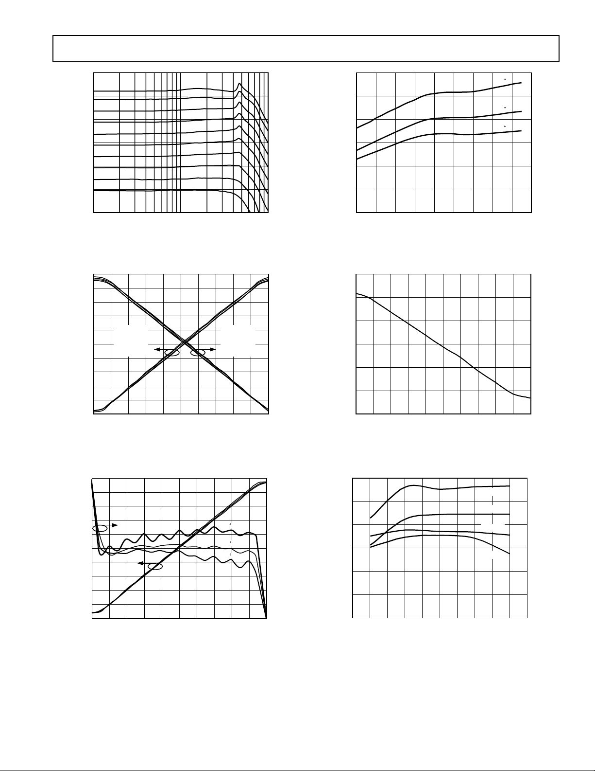
TPC 1. Gain vs. Frequency for Values of V
45
40
35
30
5
0
0 1.00.1
5
0
0 1.00.1
MODE ⴝ 5V
10MHz
70MHz
140MHz
240MHz
0.2 0.3 0.4 0.5 0.6 0.7 0.8 0.9
0.2 0.3 0.4 0.5 0.6 0.7 0.8 0.9
V
– V
GAIN
(Mode LO and Mode HI)
GAIN
V
– V
GAIN
25
20
GAIN – dB
15
10
–5
TPC 2. Gain vs. V
45
40
35
30
25
20
GAIN – dB
15
10
–5
TPC 3. Gain Conformance at 70 MHz for T –40ⴗC,
ⴗ
C, and +85ⴗC.
+25
MODE ⴝ 0V
10MHz
70MHz
140MHz
240MHz
–40 C
+25 C
+85
GAIN
2.0
1.6
1.2
0.8
0.4
C
0
–0.4
–0.8
–1.2
–1.6
–2.0
LINEARITY ERROR – dB
TPC 4. NF (re 200 Ω) vs. Frequency at Maximum Gain
60
50
40
30
20
NOISE FIGURE – dB
10
0
0 1.00.1 0.2 0.3 0.4 0.5 0.6 0.7 0.8 0.9
TPC 5. NF (re 200 ) vs. V
30
25
20
15
OIP3 – dBV rms
10
V
GAIN
– V
at 70 MHz
GAIN
10MHz
70MHz
140MHz
240MHz
37
32
27
22
17
5
0
0
0.1 0.2 0.4 0.6 0.7 0.8 0.9 1.0
0.3 0.5
V
– V
GAIN
TPC 6. OIP3 vs. V
GAIN
12
7
OIP3 – dBm (re 200⍀)
REV. 0
–5–
 Loading...